
Crystalline organic thin films for crystalline OLEDs (III): weak epitaxy growth of phenanthroimidazole derivatives with a dual inducing layer†
Xuxiang Renab,
Lunkai Liab,
Feng Zhu *ab and
Donghang Yanab
*ab and
Donghang Yanab
aState Key Laboratory of Polymer Science and Technology, Changchun Institute of Applied Chemistry, Chinese Academy of Sciences, Changchun 130022, China. E-mail: zhufeng@ciac.ac.cn
bSchool of Applied Chemistry and Engineering, University of Science and Technology of China, Hefei 230026, China
First published on 25th June 2025
Abstract
Crystalline organic thin films based on phenanthroimidazole derivatives, particularly 2FPPICz, exhibit significant potential for application in high-performance organic light-emitting diodes (OLEDs) due to their ordered molecular structure and superior optoelectronic properties. This study proposes a novel dual inducing layer structure that simultaneously achieves energy-level alignment, enhanced charge injection, and high-quality crystalline film growth. Specifically, a BP2T inducing layer is introduced between the anode and conventional BP1T layer to enhance hole injection while maintaining high-quality epitaxial growth. The BP2T layer effectively bridges the energy-level mismatch at the anode interface and reduces lattice mismatch between BP1T and 2FPPICz, facilitating the formation of large-area, continuous crystalline films. Comprehensive characterization using atomic force microscopy (AFM), X-ray diffraction (XRD), and transmission electron microscopy (TEM) confirms the improved structural coherence and epitaxial relationships within the dual inducing layers. The hole-only device demonstrates a 136% increase in current density at 1 V, highlighting the enhanced charge injection efficiency. These findings provide a strategic approach for optimizing crystalline OLED performance through a tailored dual inducing layer structure, paving the way for advanced optoelectronic applications.
Introduction
Organic crystals have garnered significant attention in the field of optoelectronics due to their highly ordered molecular arrangement, low defect density, superior charge transport properties, and thermal stability.1–4 These characteristics are pivotal for enhancing the performance of organic light-emitting diodes (OLEDs), particularly in achieving high carrier mobility and efficient light outcoupling.5–8 Among various fabrication techniques, weak epitaxy growth (WEG) has emerged as a powerful method for producing high-quality crystalline thin films.9,10 This technique enables the development of crystalline OLEDs (C-OLEDs) with exceptional luminescence properties which surpass those of amorphous thin-film OLEDs (A-OLEDs), such as low turn-on/operation voltage, high brightness, high power efficiency, low series resistance Joule heat loss ratio, etc.11–152-(4-(9H-Carbazol-9-yl)phenyl)-1-(3,5-difluorophenyl)-1H-phenanthro [9,10-d]imidazole (2FPPICz) has been successfully employed as the host material in crystalline thin films for constructing high-efficiency C-OLED systems,12,13,16 including solid-solution C-OLEDs and “hot exciton” fluorescent nanoaggregate (HENA) sensitizing C-OLEDs. Based on energy level alignment with the 2FPPICz molecule, a material called 2,5-di([1,1′-biphenyl]-4-yl)thiophene (BP1T) was chosen as both the inducing layer and hole transport layer, facilitating the epitaxial growth of 2FPPICz in the previously reported C-OLEDs.12,13,16–18 Epitaxial growth of phenanthroimidazole derivatives, specifically 2FPPICz, on BP1T inducing layers has been demonstrated and studied.19 These works revealed that the lattice matching between 2FPPICz and BP1T critically influences the morphology and structural properties of the crystalline films, with BP1T double-layers yielding larger domain sizes and lower roughness due to reduced lattice mismatch. These findings underscored the importance of optimizing the inducing layer to achieve high-performance C-OLEDs.
Based on these studies, a novel structure is proposed in this report; a dual inducing layer is utilized to achieve energy level alignment, enhanced charge injection, and high-quality thin-film growth. In typical C-OLED devices employing 2FPPICz as the host material (Fig. 1a), inducing layers were selected based on both energy level alignment and lattice matching with 2FPPICz. While the BP1T inducing layer exhibits suitable energy level matching with 2FPPICz, it presents a significant energy gap with the anode (ITO and PEDOT:PSS). This might lead to inefficient hole injection. To address this issue, we proposed a dual inducing layer that employs two distinct inducing layers to synergistically regulate energy level alignment and promote epitaxial growth of high-quality crystalline thin films. 5,5μ-[Di(1,1μ-biphenyl)-4-yl]-2,2μ-bithiophene (BP2T) exhibits a molecular structure similar to BP1T and was used as an inducing layer in a previously reported organic solar cell, with LUMO and HOMO levels of −2.8 eV and −5.3 eV, respectively. The molecular structure and crystalline stacking arrangement of BP2T are similar to those of BP1T. The single-crystal mobility obtained through epitaxial growth on inorganic single crystals reaches 0.1 cm2 V−1 s−1, while its thin-film mobility ranges from 0.03 to 0.1 cm2 V−1 s−1.20,21 Due to these properties, BP2T was selected as a dual inducing layer, which bridges the gap between ITO/PEDOT:PSS and BP1T, thereby facilitating more efficient hole injection.
 | ||
| Fig. 1 (a)–(c) Molecular structure of BP2T (a), BP1T (b) and 2FPPICz, (c) and (d) device energy levels and the exciton formation mechanism, and (e) device energy levels and the exciton formation mechanism with a dual inducing layer. | ||
In this study, we employed atomic force microscopy (AFM), transmission electron microscopy (TEM), and selected area electron diffraction (SAED) to systematically analyze the lattice matching relationship between BP2T and BP1T layers and the influence on subsequent growth of 2FPPICz crystalline thin films. The results demonstrate that the introduction of the BP2T layer not only preserves the induced molecular orientation of both BP1T and 2FPPICz, but further reduces the lattice mismatch between them. Furthermore, we fabricated single-hole devices to evaluate the hole injection efficiency, and the current density–voltage (J–V) characteristics confirmed a significant enhancement in hole injection capability with the incorporation of the BP2T layer.
This work provides a deeper understanding of a dual inducing layer and its impact on the growth of crystalline organic thin films, offering a strategic approach to designing high-performance C-OLEDs with improved hole transport and injection properties. The findings highlight the potential of tailored inducing layers in advancing the development of high-efficiency C-OLEDs.
Results and discussion
The formation of an optimal inducing layer requires a continuous thin film with a large domain size and a molecularly smooth surface.9,22,23 The molecular structures of BP1T and BP2T are shown in Fig. 1a and b. Our observations reveal that BP2T molecules undergo layer-by-layer growth with increasing deposition thickness, ultimately forming a continuous thin film. Atomic force microscopy (AFM) characterization of films with different thicknesses (Fig. S1, ESI†) demonstrates this growth behavior, with a 0.9-monolayer BP2T film exhibiting a root-mean-square (RMS) roughness of 0.835 nm. This molecularly smooth surface provides an ideal template for subsequent BP1T layer deposition.Compared with deposition on a Si/SiO2 substrate, BP1T films deposited on the BP2T monolayer show a distinct growth mode difference. AFM characterization of BP1T films with different thicknesses (Fig. S2, ESI†) on BP2T substrates reveals a distinct layer-plus-island (Stranski–Krastanov) growth mode. The first layer growth of BP1T tends to form a continuous monolayer. As the film thickness increases, the growth mode transitions to preferential island formation beginning from the second layer. Simultaneously, the emergence of well-defined strip-like crystalline domains in the BP1T film suggests the formation of an epitaxial relationship between the BP2T and BP1T layers.
X-ray diffraction (XRD) measurements provided further structural information. As shown in Fig. 2d, the out-of-plane XRD peaks of BP2T thin films and BP1T epitaxial films correspond to the (002) and (00l) reflections, respectively. Combined with their crystallographic data (the CCDC numbers of BP1T and BP2T are 1105416 and 232989, respectively),24,25 this observation confirms that both BP1T and BP2T molecules are standing upright on the substrate. This orientation of BP1T molecules remains consistent whether deposited on Si/SiO2 substrates or BP2T thin films.19 In-plane XRD analysis (Fig. 2e) shows diffraction peaks corresponding to the (110), (020), (120) reflections for BP2T, and (110), (200), (210) reflections for BP1T. Moreover, the in-plane X-ray diffraction peaks of BP1T and BP2T exhibit remarkable proximity, demonstrating a clear one-to-one correspondence between them. The precise alignment of these in-plane diffraction peaks provides evidence for lattice matching at the BP2T/BP1T interface.
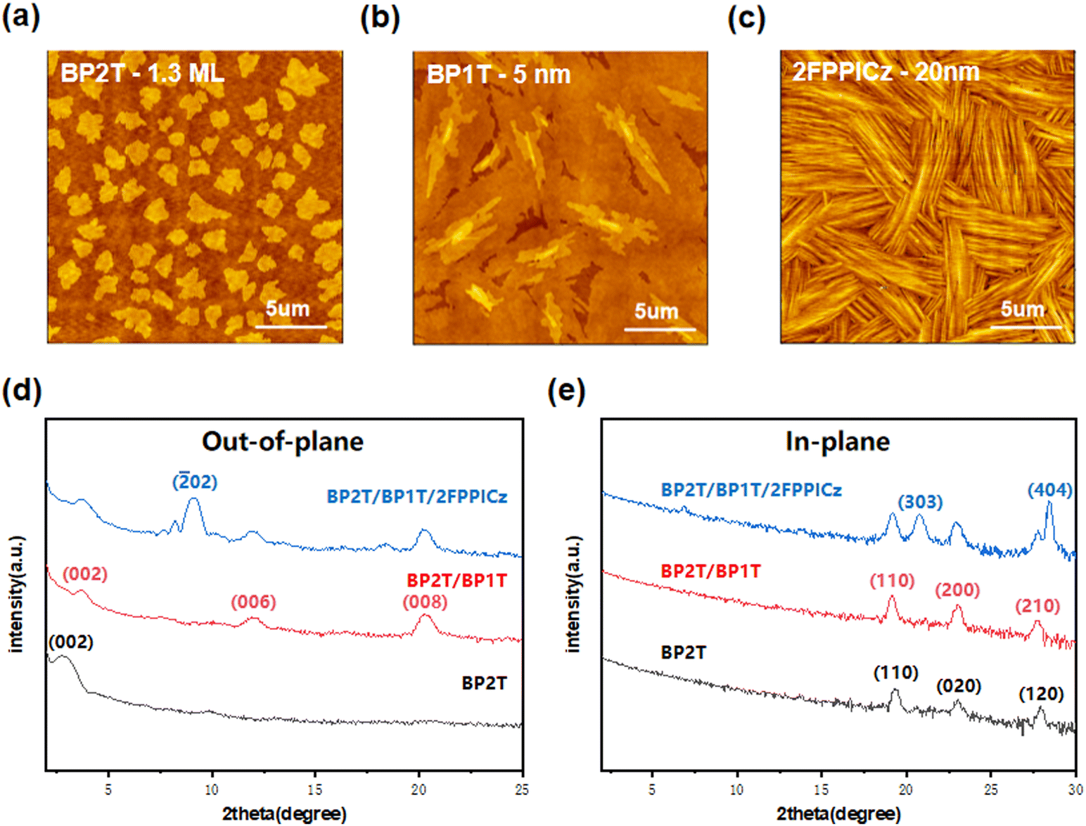 | ||
| Fig. 2 Morphologies and structures of BP2T/BP1T/2FPPICz. (a) AFM image of the 1.3-monolayer of the BP2T thin film, (b) AFM image of a 5-nm thick BP1T thin film grown on 1.3-monolayer BP2T, (c) AFM image of a 20-nm thick 2FPPICz thin film grown on the BP2T/BP1T thin film, (d) and (e) out-of-plane and in-plane X-ray diffraction (XRD) patterns of a 7 nm-thick BP2T thin film, a 5-nm thick BP1T thin film grown on 1.3-monolayer BP2T and a 20-nm thick 2FPPICz thin film grown on the BP2T/BP1T thin film. | ||
The crystallographic characteristics of the BP2T monolayer were first examined by selected area electron diffraction (SAED). As shown in Fig. 3a, the SAED pattern of BP2T exhibits a single set of diffraction spots corresponding to the (120), (020), and (100) crystallographic planes. Building upon this well-defined template, we systematically investigated the crystallographic alignment between BP2T and BP1T using transmission electron microscopy (TEM) and SAED. The analysis reveals a single set of in-plane orientations for BP1T with complete coincidence between the BP2T and BP1T diffraction patterns. This observation indicates that the BP1T epitaxial layer undergoes lattice parameter adjustment to achieve structural coherence with the underlying BP2T template. The determined epitaxial relationship follows: (001)BP2T//(001)BP1T, [010]BP2T//[100]BP1T, and [100]BP2T//[010]BP1T. According to the single crystal data of BP1T and BP2T, the mismatching between (020)BP2T and (200)BP1T planes was calculated and the interplanar spacing is presented in Table 1. The mismatching along the a* axis of BP1T is 0.16%. This low lattice mismatch enables the formation of large-area, continuous BP1T crystalline films on the BP2T monolayer, establishing an ideal substrate for subsequent 2FPPICz epitaxial growth.
 | ||
| Fig. 3 Epitaxial orientation of BP1T on BP2T. (a) Selected area electron diffraction (SAED) patterns of the 1.3-monolayer BP2T thin film, (b) selected area electron diffraction (SAED) patterns of the 5 nm-thick BP1T thin film grown on the 1.3-monolayer BP2T thin film, (c) crystal structures of BP2T as viewed along the c* axis, (d) crystal structures of BP1T as viewed along the c* axis, and (e) the schematic diagram of the BP1T epitaxially grown on BP2T along the c* axis. | ||
| Single crystal | BP2T/BP1T | BP2T/BP1T/2FPPICz | |
|---|---|---|---|
| [MismatchingBP1T/2FPPICz% = (|3d(101)2FPPICz − 5d(100)BP1T|)/(5d(100)BP1T)]. [MismatchingBP2T/BP1T% = (|d(020)2FPPICz − d(200)BP1T|)/(d(020)BP2T)]. | |||
| d(020)BP2T (Å) | 3.802 | 3.80 ± 0.04 | — |
| d(200)BP1T (Å) | 3.797 | 3.80 ± 0.04 | 3.75 ± 0.04 |
| d(101)2FPPICz (Å) | 12.786 | — | 12.30 ± 0.04 |
The epitaxial growth mechanism of BP1T on BP2T was elucidated through comprehensive structural analyses. The molecular arrangement of BP1T grown on BP2T can be directly deduced from the SAED patterns (as illustrated in Fig. 3b). Owing to the similar molecular structures and nearly identical stacking configurations of BP2T and BP1T in this orientation (Fig. 3c and d), the BP1T molecular growth essentially inherits the crystalline periodicity from the underlying BP2T thin film. Crystal structural analysis reveals that both BP2T and BP1T molecules adopt a vertical orientation with similar molecular packing geometries. Importantly, the XRD and SAED results confirm that the BP2T-induced orientation replicates that of BP1T films grown directly on Si/SiO2 substrates, demonstrating the robustness of this epitaxial system for controlling the 2FPPICz molecular orientation in device applications.
Based on the above results, we deposited a 20-nm-thick layer of 2FPPICz onto the dual inducing layer, which consists of a 1.3-monolayer BP2T film as the bottom layer and a 5-nm-thick BP1T film as the top layer. Thus, the final film structure, from the substrate upward, is BP2T, BP1T, and 2FPPICz. The AFM image of 2FPPICz on BP2T/BP1T is shown in Fig. 2c. The deposited 2FPPICz crystalline thin film undergone an epitaxial growth and formed strip-like crystal domain. The RMS of the 2FPPICz film is 2.92 nm. The width of these strip-like crystalline domains is measured as shown in Fig. S3 (ESI†). The average widths of the 2FPPICz crystals on the BP2T/BP1T layer are within the range of 400 nm to 600 nm and on BP1T are within the range of 500 nm to 600 nm.19 These data represent the maximum achievable domain length along the short-axis of 2FPPICz crystalline domains under lattice-matching constraints, demonstrating that the dual inducing layer did not induce a significant morphological change along the short-axis of 2FPPICz strip-like crystalline domains. To obtain further structural in formation, we performed out-of-plane and in-plane X-ray diffraction (XRD) measurements as shown in Fig. 2d and e. The out-of-plane diffraction peak (2θ = 9.12°) of the 20-nm thick 2FPPICz thin film on BP2T/BP1T can be assigned to 2FPPICz (![[2 with combining macron]](https://www.rsc.org/images/entities/char_0032_0304.gif) 02) reflection (CCDC number of 2FPPICz is 2106623).26 Clear Laue oscillation peaks appear near the diffraction peak corresponding to the (02) crystal plane, indicating that the 2FPPICz epitaxial film exhibits good crystallinity and structural periodicity. The in-plane diffraction peaks can be assigned to 2FPPICz (303) and (404) reflections, respectively.
02) reflection (CCDC number of 2FPPICz is 2106623).26 Clear Laue oscillation peaks appear near the diffraction peak corresponding to the (02) crystal plane, indicating that the 2FPPICz epitaxial film exhibits good crystallinity and structural periodicity. The in-plane diffraction peaks can be assigned to 2FPPICz (303) and (404) reflections, respectively.
The epitaxial relationship between 2FPPICz and the BP1T substrate has been reported in formal research. For comparing the lattice mismatching ratios and investigating the effect of the introduction of the BP2T monolayer, transmission electron microscopy (TEM) and selected area electron diffraction (SAED) are used in further study. As shown in Fig. S4 (ESI†), the diffraction patterns of BP1T and BP2T thin films still coincide and there is only one set of 2FPPICz in-plane orientation with the b* axis of 2FPPICz parallel to the b* axis of BP1T, which was revealed on the BP2T/BP1T inducing layer. The epitaxial relationship is as follows: (![[1 with combining macron]](https://www.rsc.org/images/entities/char_0031_0304.gif) 01)2FPPICz//(001)BP1T, [101]2FPPICz//[100]BP1T, and [010]2FPPICz//[010]BP1T. The long axis of the 2FPPICz molecule is parallel to the substrate, which is the advantageous orientation for the light output of OLEDs.27,28 The lattice mismatching between the (101)2FPPICz and (100)BP1T planes was calculated and the interplanar spacing is shown in Table 1. The mismatching ratio along the b* axis of 2FPPICz on the BP2T/BP1T layer is 1.6%. This relatively small reduction in the lattice mismatch ratio facilitates the formation of large-area continuous crystalline domains, which are essential to create high-performance devices.29,30 Based on the results above, we can conclude that the dual inducing layer did not change the epitaxial relationship between BP1T and 2FPPICz thin films and can contribute to the lower lattice mismatch ratio.
01)2FPPICz//(001)BP1T, [101]2FPPICz//[100]BP1T, and [010]2FPPICz//[010]BP1T. The long axis of the 2FPPICz molecule is parallel to the substrate, which is the advantageous orientation for the light output of OLEDs.27,28 The lattice mismatching between the (101)2FPPICz and (100)BP1T planes was calculated and the interplanar spacing is shown in Table 1. The mismatching ratio along the b* axis of 2FPPICz on the BP2T/BP1T layer is 1.6%. This relatively small reduction in the lattice mismatch ratio facilitates the formation of large-area continuous crystalline domains, which are essential to create high-performance devices.29,30 Based on the results above, we can conclude that the dual inducing layer did not change the epitaxial relationship between BP1T and 2FPPICz thin films and can contribute to the lower lattice mismatch ratio.
To verify the influence of the dual inducing layer on hole injection efficiency, we fabricated a hole-only device and characterized its electrical properties. The structure of the device is shown in Fig. 4a. An indium tin oxide (ITO) substrate and a 40-nm-thick poly(3,4-ethylenedioxythiophene):polystyrene sulfonate (PEDOT:PSS) layer were used as the anode and hole injection layer, respectively. A 3-nm-thick BP2T and a 7-nm-thick BP1T were deposited on PEDOT:PSS as the inducing layer. A 50-nm-thick 2FPPICz was deposited on the BP1T layer. After forming a 2FPPICz epitaxial crystalline thin film, we deposited a 10-nm-thick MoO3 to transport holes and block electrons due to its hole-transport ability and energy level. Finally, a 120-nm-thick Al was deposited on MoO3 as a cathode. Meanwhile, another hole-only device was fabricated with the same growth conditions and structure, except for the omission of the BP2T layer for comparison as shown in Fig. 4b. The current density–voltage (J–V) characteristics of two single-carrier hole-only devices were systematically investigated. The device incorporating the BP2T interlayer demonstrates a significantly enhanced slope in its J–V curve compared to the BP2T-free counterpart. The incorporation of the BP2T interlayer significantly improves hole injection efficiency in hole-only devices, particularly under low-voltage operation conditions (0–3 V). At an applied bias of 1 V, the current density of the BP2T-containing device reaches 286.66 mA cm−2, representing a 136% enhancement compared to that of the control device without BP2T (121.21 mA cm−2, Fig. 4c). This marked improvement stems from the graded energy-level alignment enabled by the BP2T interlayer. Through this method, the interlayer energy level alignment can be greatly improved to meet the requirements of high-efficiency crystalline organic light-emitting diodes (C-OLEDs).
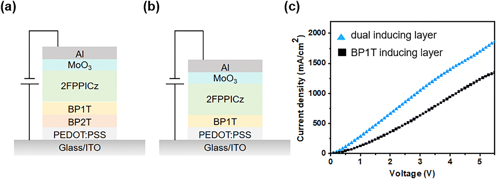 | ||
| Fig. 4 Structures and characterization of hole-only devices. (a) Structures of hole-only devices with BP2T layers, (b) structures of hole-only devices without BP2T layers, (c) the current density–voltage (J–V) characteristics. | ||
Conclusions
In conclusion, we have demonstrated a rationally designed dual inducing layer that simultaneously resolves three fundamental challenges in crystalline organic optoelectronics: (1) interfacial energy-level alignment, (2) charge injection efficiency, and (3) defect-suppressed epitaxial growth. By this method, we can concurrently address electronic and crystallographic requirements. In this paper, we investigated the morphology of a BP1T thin film on a BP2T substrate and epitaxial relationship between them by using atomic force microscopy (AFM), X-ray diffraction (XRD), transmission electron microscopy (TEM) and selected area electron diffraction (SAED). When deposited on the BP2T monolayer, the BP1T molecules stand upright on the substrate formed by intruding H atoms of the BP2T substrate. The b* axis of BP1T is parallel to the a* axis of BP2T, and the a* axis of BP1T is parallel to the b* axis of BP2T. Due to the small lattice mismatch between them, a large-size domain continuous crystalline BP1T thin film can be deposited on the BP2T substrate, which also serves as an inducing layer of 2FPPICz. According to the results of morphology and structure characterization, the dual inducing layer did not change the epitaxial relationship and further reduced the lattice mismatch between BP1T and 2FPPICz. Attributed to the optimized interlayer energy-level alignment, the effective enhancement of current density in the hole-only device demonstrates improved hole injection at the anode side. By employing this strategy, we demonstrate that a precisely designed dual inducing layer with a suitable energy-level alignment can collectively address critical challenges in hole injection for high-performance crystalline organic light-emitting diodes (C-OLEDs).Experimental
Materials
BP2T, BP1T, and 2FPPICz were synthesized using the previously reported method.31,32 All materials were purified twice by thermal gradient sublimation before usage.Fabrication and characterization of the film and device
The Si/SiO2 substrate was wiped with absorbent cotton moistened with acetone and cleaned with acetone, alcohol, and deionized water three times, desiccated in high-purity nitrogen, and dried in a baking oven at 120 °C. After that, the Si/SiO2 substrate was fixed with clamps and was kept into a vacuum chamber at a pressure of below 10−4 Pa. The BP2T thin film was deposited on the Si/SiO2 substrate at a substrate temperature of 150 °C. The BP1T and 2FPPICz thin films were deposited at a substrate temperature of 102 °C. Both the BP2T and BP1T thin films were deposited at an evaporation rate of about 2–3 Å min−1 and the 2FPPICz thin film was deposited on the BP1T thin films at an evaporation rate of about 3–4 Å min−1. The ITO substrate was first purged with a detergent and then ultrasonicated in acetone, ethanol and detergent water in sequence for 30 min. After that, the ITO substrate was dried in a baking oven at 120 °C and then treated with oxygen plasma for 15 min. PEDOT:PSS was spin-coated on the ITO substrate at 4000 rpm for 30 s to modify the anode and then dried in a baking oven at 120 °C for 30 min before usage. Then, ITO was transferred into a vacuum chamber at a pressure of under 10−4 Pa. BP2T, BP1T and 2FPPICz thin films were deposited on ITO under the same conditions as on Si/SiO2. The morphologies of the thin films were observed using an atomic force microscope (AFM SPI 3800/SPA, 300 HV, Seiko Instruments Inc., Japan) with tapping mode. A thin-film diffractometer (Bruker D8 Discover) with Cu Kα radiation (λ = 1.54056 Å) was used to collect the out-of-plane X-ray diffraction (XRD) data in the locked coupled mode. And a Rigaku SmartLab X-ray diffraction instrument was used to acquire the in-plane XRD patterns (λ = 1.54056 Å).Fabrication and characterization of TEM samples
At first, a carbon film was thermally evaporated onto the thin film deposited on the Si/SiO2 substrate as the supporting layer using an ETD-800C type small thermal evaporation coating instrument (Vision Precision Instruments Inc., China) to prevent the thin film from shattering when separated from the Si/SiO2 substrate. And then, because of the different hydrophobicity and expansion coefficient between the sample and the Si/SiO2 substrate, we can separate the thin film from the substrate and use a 400 mesh copper grid to capture the sample floating on the surface of the 10% HF solution. After that, the copper grid was placed on a filter paper until it dried. The selected area electron diffraction (SAED) patterns were acquired with a transmission electron microscope (JEOL JEM-1400) at 120 kV, and the corresponding electron micrographs were obtained under bright field conditions.Author contributions
F. Z. and D. H. Y. initiated and designed the research. X. X. R. carried out the growth and characterization of crystalline thin films and single-hole devices. L. K. L. assisted in the characterization of single-hole devices. F. Z. and D. H. Y. supervised the project. All authors discussed the results, analyzed the data and prepared the manuscript.Conflicts of interest
There are no conflicts to declare.Data availability
The crystallographic data for 2FPPICz, BP1T and BP2T were retrieved from the Cambridge Crystallographic Data Centre (CCDC) under deposition numbers 2106623, 1105416 and 232989, respectively. The other data that support the findings of this study are available within the article and its ESI.†Acknowledgements
This work was funded by the National Key R&D Program of China (Grant No. 2023YFB3608800 to F. Z.) and the National Natural Science Foundation of China (Grant No. 52373198 to F. Z.).Notes and references
- M. Pope, H. P. Kallmann and P. Magnante, J. Chem. Phys., 1963, 38, 2042–2043 CrossRef CAS.
- M. O'Neill and S. M. Kelly, Adv. Mater., 2011, 23, 566–584 CrossRef PubMed.
- J. L. Yang, D. H. Yan and T. S. Jones, Chem. Rev., 2015, 115, 5570–5603 CrossRef CAS PubMed.
- C. L. Wang, H. L. Dong, L. Jiang and W. P. Hu, Chem. Soc. Rev., 2018, 47, 422–500 RSC.
- X. T. Zhang, H. L. Dong and W. P. Hu, Adv. Mater., 2018, 30, 1801048 CrossRef PubMed.
- R. Ding, M. H. An, J. Feng and H. B. Sun, Laser Photonics Rev., 2019, 13, 1900009 CrossRef CAS.
- Y. Watanabe, H. Sasabe and J. Kido, Bull. Chem. Soc. Jpn., 2019, 92, 716–728 CrossRef CAS.
- Y. L. Shi, M. P. Zhuo, X. D. Wang and L. S. Liao, ACS Appl. Nano Mater., 2020, 3, 1080–1097 CrossRef CAS.
- H. B. Wang, F. Zhu, J. L. Yang, Y. H. Geng and D. H. Yan, Adv. Mater., 2007, 19, 2168–2171 CrossRef CAS.
- J. L. Yang and D. H. Yan, Chem. Soc. Rev., 2009, 38, 2634–2645 RSC.
- J. J. Yang, W. T. Zheng, D. H. Hu, F. Zhu, Y. G. Ma and D. H. Yan, Adv. Sci., 2023, 10, 2203997 CrossRef CAS PubMed.
- J. J. Yang, D. H. Hu, F. Zhu, Y. G. Ma and D. H. Yan, Sci. Adv., 2022, 8, eadd1757 CrossRef CAS PubMed.
- P. F. Sun, D. Liu, F. Zhu and D. H. Yan, Nat. Photonics, 2023, 17, 264–272 CrossRef CAS.
- Y. J. Liu, X. D. Wang, F. Zhu, Y. Wang and D. H. Yan, Adv. Electron. Mater., 2024, 10, 2300616 CrossRef CAS.
- Y. J. Liu, F. Zhu, Y. Wang and D. H. Yan, Light: Sci. Appl., 2024, 13, 86 CrossRef CAS PubMed.
- J. H. Xin, P. F. Sun, F. Zhu, Y. Wang and D. H. Yan, J. Mater. Chem. C, 2021, 9, 2236–2242 RSC.
- W. T. Zhen, F. Zhu and D. H. Yan, Org. Electron., 2024, 135, 107150 CrossRef.
- S. Y. Zou, S. Zhou, C. L. Li, F. Zhu, Y. Wang and D. H. Yan, ACS Appl. Mater. Interfaces, 2025, 8084–8094 CrossRef CAS PubMed.
- D. Liu, F. Zhu and D. H. Yan, RSC Adv., 2023, 13, 15586–15593 RSC.
- M. Ichikawa, H. Yanagi, Y. Shimizi, S. Hotto, N. Suganuma, T. Tikoyama and Y. Taniguchi, Adv. Mater., 2002, 14, 1272–1275 CrossRef CAS.
- S. Hotta, M. Goto, R. Azumi, M. Inoue, M. Ichikawa and Y. Taniguchi, Chem. Mater., 2004, 16, 237–241 CrossRef CAS.
- X. L. Qiao, L. Z. Huang, J. D. Zhang, H. K. Tian, Y. H. Geng and D. H. Yan, J. Phys. Chem. B, 2012, 116, 1812–1818 CrossRef CAS PubMed.
- L. Z. Huang, F. Zhu, C. F. Liu, U. Treske, M. Grobosch, H. K. Tian, J. D. Zhang, Y. H. Geng, M. Knupfer and D. H. Yan, Adv. Funct. Mater., 2012, 22, 4598–4607 CrossRef CAS.
- S. Hotta and M. Goto, Adv. Mater., 2002, 14, 498–501 CrossRef CAS.
- I. Paterson, K. Ashton, R. Britton and H. Knust, Org. Lett., 2003, 5, 1963 CrossRef CAS PubMed.
- D. Liu, F. Zhu and D. H. Yan, J. Mater. Chem. C, 2022, 10, 2663–2670 RSC.
- D. Yokoyama, J. Mater. Chem., 2011, 21, 19187–19202 RSC.
- T. D. Schmidt, T. Lampe, M. R. D. Sylvinson, P. I. Djurovich, M. E. Thompson and W. Brütting, Phys. Rev. Appl., 2017, 8, 037001 CrossRef.
- J. Fraxedas, Adv. Mater., 2002, 14, 1603–1614 CrossRef CAS.
- V. Coropceanu, J. Cornil, D. A. da, S. Filho, Y. Olivier, R. Silbey and J. L. Br das, Chem. Rev., 2007, 107, 926–952 CrossRef CAS PubMed.
- S. Hotta, H. Kimura, S. A. Lee and T. Tamaki, J. Heterocycl. Chem., 2000, 37, 281–286 CrossRef CAS.
- J. H. Xin, Z. Q. Li, Y. J. Liu, D. Liu, F. Zhu, Y. Wang and D. H. Yan, J. Mater. Chem. C, 2020, 8, 10185–10190 RSC.
Footnote |
| † Electronic supplementary information (ESI) available. See DOI: https://doi.org/10.1039/d5tc01750e |
| This journal is © The Royal Society of Chemistry 2025 |