DOI:
10.1039/C5RA13135A
(Paper)
RSC Adv., 2015,
5, 71778-71784
Influence of interface properties on charge density, band edge shifts and kinetics of the photoelectrochemical process in p-type NiO photocathodes†
Received
6th July 2015
, Accepted 11th August 2015
First published on 14th August 2015
Abstract
Nickel oxide as one of the few p-type semiconductors has great potential applications in the construction of photovoltaics and solar fuel production devices. The present work focuses on understanding the surface structure of NiO by controlling the surface Ni3+ species (e.g. NiO(OH)) that influence the electrochemical process at the NiO/liquid electrolyte interface. With the aid of the Mott–Schottky method, electrochemical impedance spectroscopy and photocurrent–voltage correlation testing, various NiO surface structures were correlated with observed changes in the band energies, energetic distributions of the trap states densities, charge interface transfer, charge transport, and as a result the p-type DSSC device performances. The primary results demonstrate that the NiO(OH) species act as recombination centers and cause worse interface recombination. Furthermore, we also report an effective way of reducing the surface NiO(OH) structures by a Ni(CH3COOH)2 post-treatment method, resulting in a 31.3% increase in the photovoltaic performance. Our work provides good guidance for the design and fabrication of solar energy-related devices employing NiO electrodes.
1. Introduction
Recently, p-type oxide semiconductors have become a more active field of research because integrating p-type oxide cathodes with n-type oxide anodes to produce tandem photovoltaic devices will improve the performance and reduce the cost of solar harvesting systems.1,2 Nickel oxide (NiO) is a promising candidate for wide band gap p-type semiconductors.3 Usually, NiO is a non-stoichiometric crystal exhibiting p-type characteristics through hole transport, which originates from nickel vacancies and/or oxygen interstitials.4–7 Due to this interesting combination of electrical and optical properties, NiOx has attracted attention as an electrode material for electrochromic windows,8,9 optoelectronic devices,6 dye-sensitized solar cells, photoelectrochemical water splitting10,11 and photoelectrochemically produced chemical fuels.12
Likewise with n-type solar energy-related devices, the essential processes of photogeneration, separation and recombination of charge carriers in p-type semiconductors all occur primarily at the heterointerface, such as in the NiO/organic photoactive layer (NiO/P3HT),13 NiO/organic emitting layer (NiO/CBP and Ir-(mppy)3),6 NiO/organic–inorganic hybrid photoactive layer (NiO/CH3NH3PbI3)14 or NiO/liquid electrolyte (NiO/acetonitrile, NiO/water etc.). Thus the interfacial energetics and kinetics of these heterointerfaces are of paramount importance in determining device performance.15
It is known that NiOx materials have complex chemical structures (e.g. NiO, Ni2O3), which are susceptible to bonding with many types of atmospheric molecules, as well as forming several hydroxide structures (e.g. Ni(OH)2, NiO(OH)).6,16,17 Greiner et al. found that the surface properties of NiO can affect the organic energy-level alignment at the NiO/organic hole-transport material (α-NPD) interface.18 Recently, Wang et al. have reported that the formation of NiO(OH) at the NiO/P3HT interface leads to an increase in the work function, resulting in enhanced polymer solar cell performance.19 Liu et al. found that more nickel oxyhydroxide species existing at the NiO/organic emitting layer interface give an organic light-emitting device a higher hole injection and light-emitting efficiency.20 However, for electrochemical systems with nanoporous NiOx/liquid electrolyte interfaces, few researchers have studied the chemically resolved surface electronic structures of their electrodes and the related influences on interfacial energetics, charger carrier transfer and relaxation dynamics, as well as on charge recombination rates.
In this work, our goal is to gain a deeper understanding of the nature of the NiO surface changes that influence the electrochemical processes at NiO/liquid electrolyte interfaces. Here we adopted post-treatments such as thermal and UV-ozone methods to control the NiO structure, as well as reporting a series of characterizations of NiOx/liquid interfaces and establishing the relationships between the complex surface chemistries of the NiO films and their band energies, the energetic distributions of their trap states densities and their charge transfer rates, which are relevant to p-type DSSCs. In addition, investigations into the current density–voltage (J–V) properties and device performances, employing the bare and post-treatment NiO films, help us to establish the key influence of the interface structure on the kinetics of the photoelectrochemical processes occurring in p-type DSSCs, as well as clarifying what kind of NiO film surface structure leads to a good photovoltaic performance. Finally, we find which surface or interface treatment methods eliminate or passivate surface defects, resulting in an enhancement of the photovoltaic performance.
2. Experimental section
2.1 Preparation of the bare and post-treatment NiO photocathodes
A precursor solution of NiO was prepared by mixing NiCl2 (1 g), co-polymer F108 (1 g), Milli-Q water (3 g) and ethanol (6 g) according to the literature.21 The as-prepared NiO films were made by a doctor-blading method on FTO (8 Ω) and dried at room temperature for at least 30 min, followed by sintering in an oven at 450 °C for 30 min, these three steps were repeated three times (NiO sample). To study how changes to the surface of the NiO film affect the electrochemical process, three designs were taken into account: (i) one further calcination at 450 °C for 30 min (NiO–S sample), (ii) placing the NiO film in a UV-ozone cleaning machine for 30 min (NiO–ozone sample) and (iii) applying the NiO film through soaking in a 20 mM Ni(CH3COOH)2 water solution for 30 min at 70 °C, followed by a water rinse and drying at 70 °C (NiO-Ac sample). The thickness (d) of all resulting NiO films was 1.1 ± 0.02 μm and the active area was 5.0 mm × 5.0 mm.
2.2 Fabrication of p-type DSSCs
To study the relationship between the complex surface chemistry of a NiO photocathode and the kinetics of the photoelectrochemical process, the resulting NiO films as photocathodes were assembled into p-type DSSCs. Firstly, the resulting NiO films were heated to 110 °C for 30 min, before being immersed in a C343 dye solution (0.3 mM in acetonitrile) for 16 h. The counter electrodes were platinized by thermal decomposition of H2PtCl6 from isopropanol on FTO at 450 °C for 30 min. A 60 μm meltonix polymer spacer (Solaronix) was used as the primary sealing material. Then, an electrolyte composed of 1.0 M LiI and 0.1 M I2 in acetonitrile solvent was injected through a hole predrilled into the counter electrode. The hole was then sealed with a glass slide.
2.3 Characterization
The morphology observations of the photoelectrodes were verified by electron microscopy (SEM) on a JEOL JSM-700F. X-Ray diffraction (XRD) measurements were taken on a Rigaku D/MAX-RB X-ray diffractometer using Cu Kα radiation (40 kV, 20 mA) and a secondary beam graphite monochromator to study the crystal structures of the films. X-ray photoelectron spectroscopy (XPS, Mg K-L3 = 1253.6 eV) was performed using a Perkin-Elmer PHI 5000C ESCA system equipped with a dual X-ray source and a hemispherical energy analyser. Spectra were calibrated in energy using C 1s = 284.6 eV as the reference, and the resolution was estimated as about 0.9 eV.
The Mott–Schottky (MS) plots of the bare NiO and post-treated NiO films were measured in aqueous electrolyte using a PGSTAT 128N potentiostat (Switzerland, Autolab). The measurements were carried out in a glass electrolytic cell, using a three-electrode configuration. The electrolyte used was aqueous 0.1 M PB (a solution of 0.2 M sodium dihydrogen phosphate mixed with 0.2 M sodium hydrogen phosphate) with 1 M potassium chloride as the supporting electrolyte. The pH of the electrolyte was adjusted to 7.0. The reference electrode was Ag/AgCl in saturated KCl, and a porous graphite stick was used as the counter electrode. Nitrogen was passed through the electrolyte for 15 min to remove any dissolved oxygen.
After the assembly of the cell, the electrochemical impedance was measured with a PGSTAT 128N potentiostat (Switzerland, Autolab) in the frequency range of 1 × 10⁵ to 1 × 10⁻¹ Hz. The AC amplitude was 10 mV. The working electrode was connected to the NiO electrode, and the counter and reference electrodes were connected to the platinized counter electrode. The cells were measured in the dark at various potentials. The EIS data was analyzed using Nova software with the transmission line equivalent circuit. The fitting results and detailed explanations can be found in the ESI.† The photovoltaic properties were measured using a Keithley 2400 Source Meter under the irradiation of simulated sunlight (100 mW cm−2) provided by an Oriel Sol 3A Class AAA solar simulator with an AM 1.5 filter.
3. Results and discussion
3.1 Surface chemical structure
X-ray photoemission spectroscopy (XPS) was used to characterize the various different oxidation states of Ni in the NiO film, which can probe changes in the near surface composition of the modified NiO photocathode. Fig. 1 and 2 show the Ni 2p and O 1s XPS spectra of the bare and modified NiO films. All samples contain the main peaks of Ni 2p3/2 at ∼853.7 eV and O 1s at ∼529.3 eV, which correspond to the stoichiometric NiO.16,22–24 To further investigate the species, the shoulder peaks of the Ni 2p3/2 signals were fitted with signals from Ni(OH)2 peaks at ∼855.1 eV and NiO(OH) peaks at ∼856.0 eV (fitting results given in Fig.1 and Table 1).24 As shown in Table 1, the number of NiO(OH) species in the NiO film reduced after the additional thermal treatment. In particular, the peaks for the surface Ni3+ species (e.g. the NiO(OH) species) in the NiO–S sample film were too weak to deconvolute. In comparison to the bare NiO film, the Ni 2p spectrum shifts to a higher binding energy after the UV-ozone treatment. As shown in Table 1, the calculated content of NiO(OH) species in the NiO–ozone sample shows an obvious increase. Accordingly, the O 1s spectrum (as shown in Fig. 2) of the NiO–ozone sample shows a dramatic change compared with the NiO and NiO–S samples, with the shoulder peak for the NiO(OH) component becoming more pronounced.16 Both of these results prove that the UV-ozone treatment introduced more dipolar NiO(OH) species onto the NiO film surface. Obviously, post-treatments such as thermal or UV-ozone treatment can influence the surface chemical structure of a NiO film, and the effect of these surface chemical structure changes on p-type DSSC device performance will be discussed below.
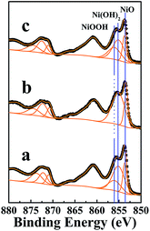 |
| | Fig. 1 Ni 2p spectra for the NiO films, from bottom to top: (a) NiO, (b) NiO–S and (c) NiO–ozone. Raw data is given by (●) and the fitted components by orange lines. | |
 |
| | Fig. 2 O 1s spectra for the NiO films, from bottom to top: (a) NiO, (b) NiO–S and (c) NiO–ozone. Raw data is given by (●) and the fitted components by orange lines. | |
Table 1 Surface analysis by XPS: spectra for the bare and post-treatment NiO films
| sample |
O 1s |
Ni 2p3/2 |
| NiO (529)a [eV] |
Ni(OH)2 (530.7–531.3)a [eV] |
NiO(OH) (532)a [eV] |
NiO (853.7–854.1)b [eV] |
Ni(OH)2 (854.9–855.6)b [eV] |
NiO(OH) (856.4)b [eV] |
(NiO![[thin space (1/6-em)]](https://www.rsc.org/images/entities/char_2009.gif) :Ni(OH)2:NiO(OH))c :Ni(OH)2:NiO(OH))c |
| The peak position for O 1s obtained from the literature.42,43 The peak position for Ni 2p3/2 obtained from the literature.16,44,45 The percentage composition of NiO(OH) was calculated from the Ni 2p3/2 fitting data. The ratio is the value of NiO:Ni(OH)2. |
| NiO |
529.23 |
530.93 |
— |
853.68 |
855.13 |
856.00 |
1:2.15:1.03 |
| NiO–S |
529.00 |
530.76 |
— |
853.44 |
855.14 |
— |
1:3.44:—d |
| NiO–ozone |
529.39 |
530.87 |
532.33 |
853.83 |
855.13 |
856.01 |
1:2.29:1.47 |
3.2 Band-edge movement and acceptor density
Further analysis of the energy band structures of the bare and post-treatment modified NiO films was performed using the Mott–Schottky (MS) equation:25| | |
1/CSC2 = −2(Eapp − Efb − kBT/e)/(eε0κNAA2)
| (1) |
where CSC, e, ε0, κ, Eapp, Efb, kB, T, NA and A are the capacitance, fundamental charge constant, vacuum permittivity, dielectric constant, applied potential bias, flat-band potential, Boltzmann constant, temperature, density of acceptors within the space charge region and effective surface area of the semiconductor, respectively. Plotting 1/CSC2 vs. the applied potential Eapp enables the estimation of NA and Efb, as shown in Fig. 3 and Table 2. The linear parts of the MS plots reveal that the flat-band potentials (listed in Table 2) are 0.40, 0.44 and 0.38 V vs. NHE for the NiO, NiO–S and NiO–ozone samples, respectively. A larger slope represents a lower acceptor density (NA). As shown in Table 2, the NiO–ozone sample shows the highest acceptor density (NA = 8.44 × 1018 cm−3), followed by the NiO sample (NA = 7.75 × 1018 cm−3) and the NiO–S sample (NA = 7.56 × 1018 cm−3). In other words, the NiO–S sample exhibits a positive shift in Efb, compared with the NiO sample, which is attributed to the decreased surface states following additional thermal treatment. In the case of the NiO–ozone sample, the more dipolar nickel oxyhydroxide (NiO(OH)) species added through the UV-ozone treatment affected the chemical environment of the NiO-solution interface, leading to an obvious negative movement of Efb. Since the Efb is associated with the Fermi level of NiO, as a result, the movement of Efb will affect the open circuit of DSSCs.26,27
 |
| | Fig. 3 Mott–Schottky plots for the NiO, NiO–S, and NiO–ozone films against an aqueous electrolyte containing 0.1 M PB (0.2 M NH2PO4 and 0.2 M Na2HPO4) and 1 M KCl with a pH adjusted to 7.0. | |
Table 2 Values of acceptor-state densities and apparent flat-band potentials for the bare and post-treatment NiO films
| Sample |
NA [ × 1018 cm−3] |
Efb [V vs. NHE] |
| NiO |
7.75 |
0.40 |
| NiO–S |
7.56 |
0.44 |
| NiO–ozone |
8.44 |
0.38 |
3.3 Charge transport and recombination
3.3.1 General description of impedance spectroscopy. To study the relationship between the complex surface chemistry of a NiO photocathode and the kinetics of the photoelectrochemical process occurring in p-type DSSCs, cells employing the bare and modified NiO photocathodes were fabricated. Then, electrochemical impedance spectroscopy (EIS) was carried out in the dark at different bias voltages (Vapp). Their typical Nyquist and Bode plots are shown in Fig. 4. In the Nyquist plots, two semicircles are clearly visible, a smaller one in the high frequency region corresponding to charge transfer at the electrolyte/counter electrode interface, and a larger one in the low frequency region resulting from hole transfer at the NiO/dye/electrolyte interface (recombination resistance) and hole transport in the NiO photocathode (hole transport resistance).28–30 In the Bode plots, the frequency peak position, which is related to charge transfer at the NiO/dye/electrolyte interface, is shifted. The peak frequency of the larger semicircle is inversely proportional to the lifetime (τh) of the hole in a photocathode. The hole lifetime, estimated from the expression τh = 1/2πfmax (fmax is the peak frequency), decreases in the order NiO–S sample > NiO sample > NiO–ozone sample. To fit the experimental data, a transmission line model was used and the corresponding parameters obtained from the equivalent circuit are listed in Table S1† and Fig. 5.
 |
| | Fig. 4 (A) Bode plots and (B) Nyquist plots of the p-type DSSCs employing the NiO, NiO–S and NiO–ozone films at a 60 mV bias in the dark. | |
 |
| | Fig. 5 (A) chemical capacitances, (B) hole recombination resistances and hole transport resistances, (C) hole lifetimes and hole transport times and (D) collection efficiencies of the devices employing bare and post-treatment NiO photocathodes as a function of the corrected voltage obtained from the impedance spectra (NiO sample: black, NiO–S sample: red and NiO–ozone sample: blue). | |
3.3.2 Chemical capacitance and trap states distribution. As shown in Fig. 5A, the chemical capacitance (Cμ) values exhibit an exponential trend as a function of the corrected potentials (Vcorr, the correction method is shown in the ESI†), which arises from the energetic distribution of the trap states density above the valence band-edge.29,31 The depth of the trap energy distribution is governed by the parameter α according to:| | |
Cμ = C0exp(qαVcorr/kBT)
| (3) |
where kB is the Boltzmann constant, T is the absolute temperature, C0 is the factor of the exponential increase and q is the elementary charge.32 α is a parameter that accounts for the depth of the trap energy distribution. As shown in Table S2,† the fits give α values ranging between 0.02 and 0.05, which are smaller than those of n-type dye sensitized solar cells for which α is reported to range between 0.2 and 0.4.33–35 Small values of α indicate broadening of the trap distribution. Thus, the wide and deep trap states energy distributions of the NiO photocathodes reveal that serious charge recombination problems are the dominant factor in the photovoltaic performance.36–38
3.3.3 Charge recombination. The interfacial recombination resistance (Rrec) at the NiO/dye/electrolyte interface is related to the recombination of photo-injected holes from the NiO valence band with reduced species in the electrolyte. As shown in Fig. 5B, the Rrec of all cells decreased exponentially with the increase in the corrected voltages (Fig. 5B), due to the increased hole densities in the valence bands.39 It also clearly shows that the cell based on the NiO–S sample shows a higher Rrec than the bare NiO cell with the same external bias. The observed higher Rrec of the NiO–S sample can be attributed to the decrease in surface defects caused by thermal treatment, which can inhibit hole back transfer from NiO to the electrolyte.In contrast, the cell employing the NiO–ozone film revealed a relatively lower Rrec compared to the bare NiO cell. The UV-ozone treatment can introduce more (NiO(OH)) species onto the NiO photocathode surface (supported by the XPS results).16 Wang et al. reported that Ni3+ is also an acceptor of electrons.40 Besides, the NiO(OH) species have dipole moments pointing toward the NiO surface. Thus, the NiO(OH) species could intensify electron injection from the reduced species in the electrolyte to NiO, and then cause the recombination of electrons with injected holes in the valence band.
3.3.4. Hole lifetime, charge transport time and collection efficiency. The hole transport resistance (Rt) values, transport times (τth) and hole lifetimes (τh) of the cells employing the bare and modified NiO photocathodes are plotted in Fig. 5B and C as a function of the corrected bias voltage. Obviously, Rt and τth for the modified NiO DSSCs do not change much following the application of thermal or UV-ozone surface treatments. Significantly, the order of decreasing τh is NiO–S sample > NiO sample > NiO–ozone sample. Generally, efficient charge collection is a prerequisite for the efficient conversion of light to electrical energy. The collection efficiency (ηcc) reflects the competition between the transport and recombination of holes, which is calculated and shown in Fig. 5D and Table S1.† It is noted that the order of decreasing ηcc is NiO–S sample > NiO sample > NiO–ozone sample.
3.4 Photovoltaic performance
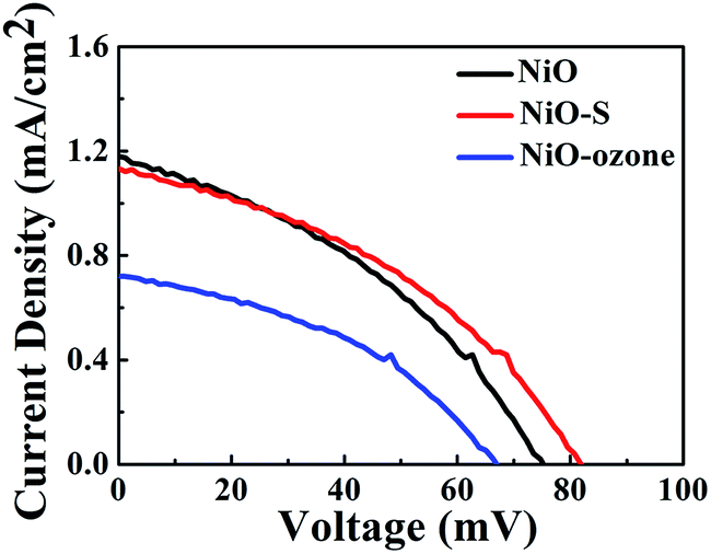
Fig. 6 and Table S3† show the current–voltage characteristics of p-type DSSCs based on the bare and modified NiO photocathodes, as measured under AM 1.5 irradiation. The reference cell (the bare NiO photocathode, NiO sample) produced a Jsc of 1.18 mA cm−2, Voc of 74 mV, and FF of 37.7, corresponding to a η of 0.032%. Additional thermal treatment (NiO–S sample) decreased the Jsc to 1.13 mA cm−2, which was explained by a reduction in the dye absorption amount from 4.07 to 3.92 × 10⁻⁸ mol cm−2. It is notable that the additional thermal treatment (NiO–S sample) markedly raised the Voc to 81 mV, resulting in a η of 0.036%. Apparently, the enhanced efficiency is ascribed to the increased Voc. Based on the EIS analysis, the higher Rrec of the NiO–S sample, as a result of effective hole collection, plays a positive role in the Voc of the cell. With regards to the surface modified NiO photocathode from UV-ozone treatment, the NiO–ozone sample exhibits an obvious decrease in Voc to 66 mV and a Jsc of 0.72 mA cm−2, leading to around a 37.5% decrease in the η (0.020%) compared with the bare NiO photocathode (0.032%). This result can be related to the fact that the low Rrec of the NiO–ozone sample leads to relatively serious interfacial charge recombination, which brings about a low Jsc and Voc.
 |
| | Fig. 6 Current–voltage characteristics of the NiO, NiO–S and NiO–ozone devices under standardized AM 1.5 illumination of 100 mW cm−2 (active area 0.25 cm2). | |
Considering the above surface microstructure and photoelectrochemical properties analyses, the surface chemistry of a NiO photocathode can be considered to determine the interface recombination resistance and play a significant role in the efficiency of p-type DSSC devices. Therefore, another important issue is to find a way to make modified NiO photocathodes with less surface defect species, especially those with the NiO(OH) structure, but with minimal negative effects on other properties such as the dye absorption amount, hole transportation, etc., which can be predicted to result in good photovoltaic performances. In present study, we employed the Ni(CH3COOH)2 post treatment method to modify the NiO photocathode. Compared with the bare NiO photocathode (NiO sample), the Ni(CH3COOH)2 post treatment method successfully reduced the surface NiO(OH) structure without effects on the crystal structure, morphology and dye absorption ability (supported by XRD, SEM and XPS results, as shown in Fig. S1–3 and Table S4†). Thus, the Ni(CH3COOH)2 post treatment method could passivate the surface defect states and prevent traps from playing a part in the hole back reaction. In relation to the photovoltaic performance (as shown in Fig. S4 and Table S3†), the cell employing the Ni(CH3COOH)2 surface modified NiO photocathode exhibited an obvious increase in Voc to 80 mV and Jsc to 1.45 mA cm−2, which lead to the cell efficiency reaching η = 0.042% (Fig. S5 and Table S3†).
Although after treatment both the open-circuit voltage and short-circuit current density seem rather small, we consider that another tempting direction to further improve the energy conversion efficiency is to construct an efficient p-type sensitizer. Recently, Wang huan et al. have reported that a p-type DSSC based on organometal halide perovskite-sensitized NiO has gained an enhanced short current density (9.47 mA cm−2) and efficiency (0.71%).41 If a p-type semiconductor is to be adopted in a working solar cell with both a photoanode and a photocathode, an optimized NiO surface and the use of an efficient p-type sensitizer are both necessary to further improve the performance.
4. Conclusion
In this present work, we provided a good understanding of the surface chemistries, surface compositions, interfacial energetics and kinetics of bare and post-treated NiO films, by combining the results from XPS, MS plots and EIS. The results will help us to elucidate the relationship between the complex surface chemistries of NiO photocathodes and the kinetics of the photoelectrochemical processes occurring in solar energy-related devices. The study herein shows that more NiO(OH) species on the NiO film surface can be introduced by a UV-ozone post-treatment, while these surface Ni3+ species (e.g. NiO(OH) species) are obviously reduced by additional thermal treatment. Mott–Schottky measurements demonstrate that as more dipolar NiO(OH) species formed, the acceptor density increased in the NiO film. Moreover, the more dipolar NiO(OH) species added through UV-ozone treatment lead to an obvious negative movement of Efb. Another remarkable result was that the NiO photocathode had a deeper trap states energy distribution than those of n-type DSSCs, which as a result brought about more serious charge recombination problems, proving that understating and controlling the NiO surface and/or interface structure are dominant factors in the performances of photovoltaic devices. Furthermore, EIS analysis showed that the NiO(OH) species act as recombination centers, and as a result worsen the interface recombination. Thus, modified NiO photocathodes with less surface defect species, especially those with the NiO(OH) structure, can be predicted to result in excellent photovoltaic performances. We also offer an effective way of reducing the surface NiO(OH) structures by a Ni(CH3COOH)2 post-treatment method, resulting in a 31.3% increased photovoltaic performance.
Acknowledgements
The authors acknowledge the support of the National Natural Science Foundation of China (51302164, 51472154, 51202138 and 51202140), Natural Science Foundation of Shanghai (13ZR1417100, 12ZR1410500), Shanghai Municipal Science and Technology Commission (13DZ2292100), Baoshan District Science and Technology Commission of Shanghai (bkw2013142), and the Professional and Technical Service Platform for Designing and Manufacturing of Advanced Composite Materials, Shanghai.
Notes and references
- F. Odobel, Y. Pellegrin, E. A. Gibson, A. Hagfeldt, A. L. Smeigh and L. Hammarström, Coord. Chem. Rev., 2012, 256, 2414–2423 CrossRef CAS PubMed.
- F. Odobel, L. Le Pleux, Y. Pellegrin and E. Blart, Acc. Chem. Res., 2010, 43, 1063–1071 CrossRef CAS PubMed.
- F. Odobel and Y. Pellegrin, J. Phys. Chem. Lett., 2013, 4, 2551–2564 CrossRef CAS.
- H. T. Nguyen, H. Jeong, J. Y. Park, Y. H. Ahn and S. Lee, ACS Appl. Mater. Interfaces, 2014, 6, 7286–7291 CAS.
- Z. L. Zhu, Y. Bai, T. Zhang, Z. K. Liu, X. Long, Z. H. Wei, Z. L. Wang, L. X. Zhang, J. N. Wang, F. Yan and S. H. Yang, Angew. Chem., Int. Ed., 2014, 53, 12571–12575 CAS.
- S. Y. Liu, R. Liu, Y. Chen, S. H. Ho, J. H. Kim and F. So, Chem. Mater., 2014, 26, 4528–4534 CrossRef CAS.
- C. J. Flynn, E. E. Oh, S. M. McCullough, R. W. Call, C. L. Donley, R. Lopez and J. F. Cahoon, J. Phys. Chem. C, 2014, 118, 14177–14184 CAS.
- D. Y. Ma, G. Y. Shi, H. Z. Wang, Q. H. Zhang and Y. G. Li, J. Mater. Chem. A, 2014, 2, 13541–13549 CAS.
- H. Huang, J. Tian, W. K. Zhang, Y. P. Gan, X. Y. Tao, X. H. Xia and J. P. Tu, Electrochim. Acta, 2011, 56, 4281–4286 CrossRef CAS PubMed.
- C. Hu, K. Chu, Y. Zhao and W. Y. Teoh, ACS Appl. Mater. Interfaces, 2014, 6, 18558–18568 CAS.
- K. Fominykh, J. M. Feckl, J. Sicklinger, M. Döblinger, S. Böcklein, J. Ziegler, L. Peter, J. Rathousky, E.-W. Scheidt, T. Bein and D. Fattakhova-Rohlfing, Adv. Funct. Mater., 2014, 24, 3123–3129 CrossRef CAS PubMed.
- A. Bachmeier, S. Hall, S. W. Ragsdale and F. A. Armstrong, J. Am. Chem. Soc., 2014, 136, 13518–13521 CrossRef CAS PubMed.
- J. W. Wan, G. J. Fang, P. L. Qin, Q. Zheng, N. S. Liu, N. H. Sun, Y. Tu, X. Fan, F. Cheng and X. Z. Zhao, Sol. Energy Mater. Sol. Cells, 2012, 101, 289–294 CrossRef CAS PubMed.
- K. C. Wang, P. S. Shen, M. H. Li, S. Chen, M. W. Lin, P. Chen and T. F. Guo, ACS Appl. Mater. Interfaces, 2014, 6, 11851–11858 CAS.
- L. D’Amario, G. Boschloo, A. Hagfeldt and L. Hammarstrom, J. Phys. Chem. C, 2014, 118, 19556–19564 Search PubMed.
- E. L. Ratcliff, J. Meyer, K. X. Steirer, A. Garcia, J. J. Berry, D. S. Ginley, D. C. Olson, A. Kahn and N. R. Armstrong, Chem. Mater., 2011, 23, 4988–5000 CrossRef CAS.
- Z. Y. Wang, S. H. Lee, D. H. Kim, J. H. Kim and J. G. Park, Sol. Energy Mater. Sol. Cells, 2010, 94, 1591–1596 CrossRef CAS PubMed.
- M. T. Greiner, M. G. Helander, Z.
B. Wang, W. M. Tang and Z. H. Lu, J. Phys. Chem. C, 2010, 114, 19777–19781 CAS.
- F. Wang, G. Sun, C. Li, J. Liu, S. Hu, H. Zheng, Z. a. Tan and Y. Li, ACS Appl. Mater. Interfaces, 2014, 6, 9458–9465 CAS.
- S. Liu, R. Liu, Y. Chen, S. Ho, J. H. Kim and F. So, Chem. Mater., 2014, 26, 4528–4534 CrossRef CAS.
- S. Sumikura, S. Mori, S. Shimizu, H. Usami and E. Suzuki, J. Photochem. Photobiol., A, 2008, 199, 1–7 CrossRef CAS PubMed.
- D. Vlachos, M. Kamaratos and S. D. Foulias, J. Phys.: Condens. Matter, 2006, 18, 6997–7011 CrossRef CAS.
- M. A. Peck and M. A. Langell, Chem. Mater., 2012, 24, 4483–4490 CrossRef CAS.
- A. G. Marrani, V. Novelli, S. Sheehan, D. P. Dowling and D. Dini, ACS Appl. Mater. Interfaces, 2014, 6, 143–152 CAS.
- Y. Fang, X. Ai, X. Wang, Q. Wang, J. Huang and T. Wu, J. Alloys Compd., 2014, 594, 211–216 CrossRef CAS PubMed.
- E. Thimsen, A. B. F. Martinson, J. W. Elam and M. J. Pellin, J. Phys. Chem. C, 2012, 116, 16830–16840 CAS.
- A. Renaud, B. Chavillon, L. Le Pleux, Y. Pellegrin, E. Blart, M. Boujtita, T. Pauporte, L. Cario, S. Jobic and F. Odobel, J. Mater. Chem., 2012, 22, 14353–14356 RSC.
- Z. Ji, G. Natu, Z. Huang, O. Kokhan, X. Zhang and Y. Wu, J. Phys. Chem. C, 2012, 116, 16854–16863 CAS.
- Z. Huang, G. Natu, Z. Ji, M. He, M. Yu and Y. Wu, J. Phys. Chem. C, 2012, 116, 26239–26246 CAS.
- H. Yang, G. H. Guai, C. Guo, Q. Song, S. P. Jiang, Y. Wang, W. Zhang and C. M. Li, J. Phys. Chem. C, 2011, 115, 12209–12215 CAS.
- L. Peter, Acc. Chem. Res., 2009, 42, 1839–1847 CrossRef CAS PubMed.
- M. S. Góes, E. Joanni, E. C. Muniz, R. Savu, T. R. Habeck, P. R. Bueno and F. Fabregat-Santiago, J. Phys. Chem. C, 2012, 116, 12415–12421 Search PubMed.
- Q. Wang, S. Ito, M. Grätzel, F. Fabregat-Santiago, I. Mora-Seró, J. Bisquert, T. Bessho and H. Imai, J. Phys. Chem. B, 2006, 110, 25210–25221 CrossRef CAS PubMed.
- L. M. Peter, J. Phys. Chem. C, 2007, 111, 6601–6612 CAS.
- Y. Kusumawati, M. A. Martoprawiro and T. Pauporté, J. Phys. Chem. C, 2014, 118, 9974–9981 CAS.
- G. Natu, Z. Huang, Z. Ji and Y. Wu, Langmuir, 2012, 28, 950–956 CrossRef CAS PubMed.
- S. Uehara, S. Sumikura, E. Suzuki and S. Mori, Energy Environ. Sci., 2010, 3, 641 CAS.
- T. A. Peiris, J. S. Sagu, K. G. Wijayantha and J. Garcia-Canadas, ACS Appl.Mater. Interfaces, 2014, 6, 14988–14993 CAS.
- X. Dou, D. Sabba, N. Mathews, L. H. Wong, Y. M. Lam and S. Mhaisalkar, Chem. Mater., 2011, 23, 3938–3945 CrossRef CAS.
- K.-C. Wang, P.-S. Shen, M.-H. Li, S. Chen, M.-W. Lin, P. Chen and T.-F. Guo, ACS Appl. Mater. Interfaces, 2014, 6, 11851–11858 CAS.
- H. Wang, X. Zeng, Z. Huang, W. Zhang, X. Qiao, B. Hu, X. Zou, M. Wang, Y.-B. Cheng and W. Chen, ACS Appl. Mater. Interfaces, 2014, 6, 12609–12617 CAS.
- L. Berkat, L. Cattin, A. Reguig, M. Regragui and J. C. Bernede, Mater. Chem. Phys., 2005, 89, 11–20 CrossRef CAS PubMed.
- D. T. Nguyen, A. Ferrec, J. Keraudy, M. Richard-Plouet, A. Goullet, L. Cattin, L. Brohan and P. Y. Jouan, Surf. Coat. Technol., 2014, 250, 21–25 CrossRef CAS PubMed.
- A. Renaud, B. Chavillon, L. Cario, L. L. Pleux, N. Szuwarski, Y. Pellegrin, E. Blart, E. Gautron, F. Odobel and S. Jobic, J. Phys. Chem. C, 2013, 117, 22478–22483 CAS.
- A. P. Grosvenor, M. C. Biesinger, R. S. Smart and N. S. McIntyre, Surf. Sci., 2006, 600, 1771–1779 CrossRef CAS PubMed.
Footnote |
| † Electronic supplementary information (ESI) available. See DOI: 10.1039/c5ra13135a |
|
| This journal is © The Royal Society of Chemistry 2015 |
Click here to see how this site uses Cookies. View our privacy policy here.