DOI:
10.1039/C4RA14222E
(Paper)
RSC Adv., 2015,
5, 9621-9626
Temperature stress on a thin film transistor with a novel BaZnSnO semiconductor using a solution process
Received
10th November 2014
, Accepted 5th January 2015
First published on 5th January 2015
Abstract
We have fabricated novel BaZnSnO-TFT using a solution process and investigated the electrical performance and temperature stability. BaZnSnO-TFT shows an improved field-effect mobility of 3.2 cm2 V−1 s−1, a subthreshold swing of 0.61 V per decade and an on/off current ratio of 2 × 10⁷ compared to those of ZnSnO-TFT. Density of state distribution of BaZnSnO and ZnSnO semiconductor has been extracted from electrical measurements. BaZnSnO-TFT shows an improved electrical performance and temperature stability due to smaller oxygen vacancies, less bulk trap density and interface state density.
1. Introduction
Recently, thin film transistors (TFTs) based on oxide semiconductors have been reported as an alternative to amorphous silicon (a-Si) TFTs due to high mobility, high stability and transparency in visible light region.1,2 Many deposition methods such as radio frequency magnetron sputtering, pulse laser deposition, and solution processes, have been reported to prepare oxide thin films. Solution-processed oxide thin films as a channel layer of TFTs are paid more attention due to simple, low cost, large area uniformity and various compositions of oxide thin films.
For realization of high performance of oxide TFTs, In-based semiconductors such as InZnO, InGaZnO, and HfInZnO, have been frequently reported.3,4 In3+ is favorable to achieve high mobility due to its special electron configuration of 4d105s0.5 However, a rare-earth indium element is expensive, toxic, and unstable in hydrogen plasma, which will enhance the fabrication cost of transistor. Sn-based oxide semiconductor has become a competitive alternative for indium because Sn4+ has a similar electron configuration with In3+ and amorphous ZnSnO-TFTs have achieved high performances comparable with InGaZnO-TFTs. In order to reduce oxygen vacancies of ZnSnO film, Si, Zr, Al element have been doped into ZnSnO film to suppress oxygen vacancies.6–8 To find more effective carrier suppressors, we have considered three important factors consisting of low standard electrode potential (SEP), larger bandgap, and low electro-negativity. For this reason, Ba is also an attractive material for carrier suppressors due to its low SEP (−2.90 V), wide bandgap (4.8 eV) and lower electro-negativity (0.89). Here, solution-processed BaZnSnO film as an active layer of TFTs was firstly reported.
The field effect mobility of oxide TFTs is acceptable for next-generation flat panel displays. Thin film transistors are affected by ambient temperature and self-heating in the work process. Thus, the device reliability including temperature instability has already limited the development of oxide TFTs into commercial electron electronic products. For commercial application, precise knowledge of the mechanism of temperature instability is necessary. Density of states (DOS) including the interfacial trap density and bulk trap density has a strong influence on temperature instability. In this work, we have fabricated a novel BaZnSnO-TFT and firstly studied the temperature instability. DOS distribution of BaZnSnO semiconductor has been extracted from electrical measurements. It provides a quantitative analysis that correlates the temperature instability of BaZnSnO-TFT to DOS parameters.
2. Experimental details
BaZnSnO thin film was prepared using zinc acetate dehydrate (Zn(CH3COO)2·2H2O), tin chloride dehydrate (SnCl2·2H2O) and barium nitrate (Ba(NO3)2). These precursors were dissolved in 2-methoxyethanol. A 0.1 M monoethanolamine (MEA) was then added in the precursor solution as a sol–gel stabilizer. The concentration of metal precursors was 0.25 M and the molar ratio was 1![[thin space (1/6-em)]](https://www.rsc.org/images/entities/char_2009.gif) :2:0.15 for Zn:Sn:Ba. The solution was stirred at 50 °C for 3 h.
:2:0.15 for Zn:Sn:Ba. The solution was stirred at 50 °C for 3 h.
A bottom-gate-type TFT was fabricated. Highly doped n-type silicon wafer with 0.01–0.025 Ω cm was used as substrate and gate electrode. A 300 nm thick SiO2 used as a gate dielectric was fabricated by thermal oxidation on the high-doped n-type silicon wafer. Prior to processing, the wafer was cleaned with a standard wet-cleaning procedure. The BaZnSnO film were prepared by spin-coating at 3000 rpm for 30 s and prebaked at 200 °C for 20 min. Subsequently, the wafer was annealed at 500 °C for 80 min in ambient air. Finally, a 60 nm thick Al film was sequentially vacuum deposited onto active layer using a metal mask to define transistor with channel width W = 1000 μm and channel length L = 200 μm.
The current–voltage characteristics of the devices were measured using an Agilent 4155C semiconductor analyzer. The capacitance measurements were conducted with an Agilent E4980A Precision LCR meter. The thickness of thin film was determined by a surface profiler (Alpha-Step IQ). X-ray diffraction (XRD) scans were measured with a Rigaku D\Max-2200 X-ray diffractometer using Cu Kα radiation. Optical properties of thin films were measured using a UV-vis spectrophotometer. The chemical bonding states of films was carried out with the X-ray photoelectron spectroscopy (XPS) (Thermo-ESCALAB 250Xl). All measurements were carried out at room temperature.
3. Results and discussion
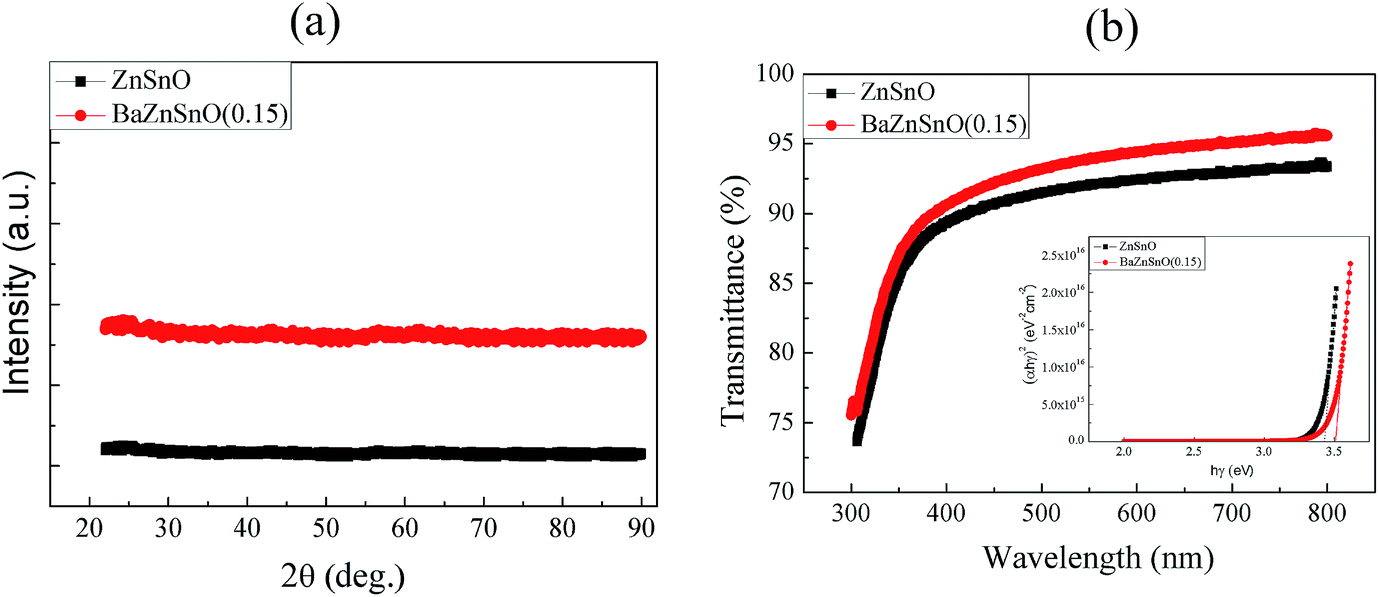
Fig. 1 (a) shows the X-ray diffraction pattern of the ZnSnO and BaZnSnO (0.15) film prepared on SiO2/Si substrate and annealed at 500 °C for 80 min. The ZnSnO film and BaZnSnO film show amorphous phase with no prominent peak. The amorphous oxide thin films have more uniform structures and smoother surfaces which could yield smooth channel/gate insulator interface. The optical transmittance spectra of ZnSnO and BaZnSnO (0.15) film on the glass substrate were characterized as shown in Fig. 1(b). The average transmittances in the range of 400–700 nm are over 87% for both films. The energy bandgap (Eg) can be obtained by using the following equation:where h is Planck's constant, γ is the frequency of incident photon, and β is energy independent constant. Eg can be obtained by extrapolating the linear portion of the (αhγ)2 and hγ plots to the energy axis, as shown in the inset of Fig. 1(b). The band gap of BaZnSnO (0.15) film is obtained to be 3.51 eV. The bandgap of undoped ZnSnO film is 3.40 eV. The broadening of band gap of BaZnSnO leads to a reduction in the electron charge carrier and an increase in the activation energy. On the other hand, the broadening of band gap of BaZnSnO film makes the climb of carrier from the valence band to the conduction band more difficult.9,10
 |
| | Fig. 1 (a) The X-ray diffraction pattern of the ZnSnO and BaZnSnO (0.15) film. (b) The optical transmittance spectra of ZnSnO and BaZnSnO (0.15) film on the glass substrate. | |
Fig. 2 shows O1s peaks of XPS spectra of ZnSnO and BaZnSnO (0.15) film. The O1s region of the XPS spectrum can be divided into three regions: low binding energy (OI, 530.7 eV), media binding energy (OII, 531.5 eV) and high binding energy (OIII, 532.5 eV). The OI peak indicates a metal–oxygen lattice peak without oxygen deficiency. Similarly, the OII and OIII are related to the O2− ions located in the oxygen deficient region in the film and bonded oxygen such as H2O, O2 on the film surface or inside thin films, respectively. The change of Vo concentration can be depicted by the peak area variation of OII component. The integral areas of OI, OII and OIII can be obtained by fitting the XPS spectra of O1s. S1, S2, and S3 represent the integral areas of OI, OII and OIII peak, respectively. Stot is the sum of the integral areas of OI, OII and OIII peak. Interestingly, S2/Stot value of BaZnSnO film is about 25.9%, which is smaller than that of the ZnSnO film (34.2%). It indicates that Ba acted as a carrier suppressor in the ZnSnO film. Ba ions are easily to form stronger chemical bonds with oxygen than Zn and Sn ions, which can attributed to the relatively high bond strength of Ba–O (562 kJ mol−1) comparing with Zn–O (395 kJ mol−1) and Sn–O (531.8 kJ mol−1). Thus, Ba can effectively suppress the formation of oxygen vacancies and lower oxygen vacancies are favorable to improve stability of thin film transistor.
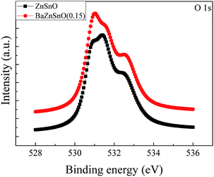 |
| | Fig. 2 O1s peaks of XPS spectra of ZnSnO and BaZnSnO film. | |
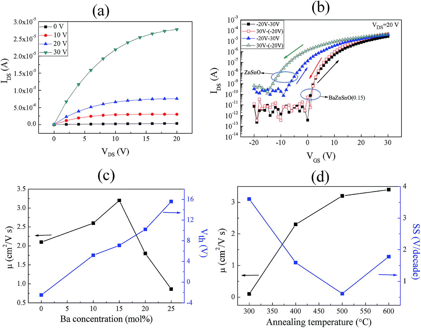
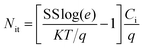
Fig. 3(a) and (b) shows the output characteristics of the BaZnSnO (0.15)-TFT tested at room temperature, respectively. The BaZnSnO-TFT shows a normally off type n-channel enhanced-mode behavior. No current crowding is observed from Fig. 3(a) indicating good ohmic contacts between BaZnSnO channel layer and Al source/drain electrode. Fig. 3(b) shows the electrical hysteresis of source-to-drain current (IDS) as a function of VGS with the fixed drain voltage (VDS) at 20 V for BaZnSnO (0.15)-TFT. The VGS is swept by 1 V increments along a forward sweep from −20 V to 30 V and along a reverse sweep from 30 V to −20 V. The clockwise hysteresis suggests that negative charge carriers are trapped at the interface between the channel and the gate insulator or injected into the gate insulator from the channel.11 The electrical hysteresis of BaZnSnO (0.15)-TFT is obviously better than that of ZnSnO-TFT. The results clearly indicate the poor stability of ZnSnO-TFTs, which could be attributed to charge trapping at the bulk and the ZnSnO/SiO2 interface. BaZnSnO (0.15)-TFT shows no obvious hysteresis, indicating that less negative charge carriers are trapped at the interface between the channel and the gate insulator or injected into the gate insulator. The result is also verified by the smaller subthreshold swing. The mobility of the BaZnSnO-TFT in the saturation region was extracted from the following equation:
| |
 | (2) |
where
IDS is the drain–source current,
W is the width of channel,
L is the length of channel,
Ci is the capacitance per unit area of the insulator layer (
Ci = 10.0 nF cm
−2),
VGS is the gate voltage,
μ is the saturation mobility and
Vth is the threshold voltage. The
Vth of the devices was determined by extrapolating the
IDS1/2 vs. VGS plot to
IDS = 0. In addition, the subthreshold swing (SS) is calculated from the subthreshold region using the following equation
| |
 | (3) |
SS is given by the maximum slope in the transfer curve. The BaZnSnO-TFT shows a
μ,
Vth,
Ion/off, and SS of 3.2 cm
2 V
−1 s
−1, 7.1 V, 2 × 10
7, and 0.61 V per decade, respectively. In addition, the maximum interfacial traps density (
Nit) can be estimated from the following equation:
| |
 | (4) |
where
k is Boltzmann constant,
q is the elementary electron charge and
T is the absolution temperature. The
Nit,max value of BaZnSnO-TFT is estimated to be 5.7 × 10
11 cm
−2, which is comparable with the published value for sputtered InGaZnO-TFT fabricated on a SiO
2-based substrate.
12,13 The low
Nitmeans that BaZnSnO-TFT has a low charge trapping at the BaZnSnO/SiO
2 interface. For comparison, ZnSnO-TFT is fabricated and electrical performance is investigated, as shown in
Fig. 3(b).
 |
| | Fig. 3 The (a) output and (b) the electrical hysteresis of the BaZnSnO (0.15)-TFT tested at room temperature. the effect of (c) Ba ratio and (d) annealing temperature on the electrical performance of BaZnSnO-TFT. | |
The effect of Ba ratio and annealing temperature on the electrical performance of BaZnSnO-TFT is investigated. The electrical performance of BaZnSnO-TFT at a VDS of 20 V for various Ba content levels is shown in Fig. 3(c). The 15 mol% Ba-doped ZnSnO-TFT has the highest saturation mobility value of 3.2 cm2 V−1 s−1. When the Ba content is 25 mol%, the saturation mobility decreases from 3.2 to 0.86 cm2 V−1 s−1. As the Ba content increases, the threshold voltage increases monotonically from −2.5 to 15.6 V. The result is attributed to the excess Ba addition results in the lower carrier concentration and the decreased conductivity of the channel layer. The saturation mobility and the subthreshold swing as a function of the annealing temperature are shown in Fig. 3(d) when the annealing temperature is increased to 300 to 600 °C, the saturation mobility increases from 0.2 to 3.4 cm2 V−1 s−1. The result is due to the increase in the number of native defects especially oxygen vacancies with the annealing temperature increasing. Unfortunately, the excess oxygen deficiencies induced by high temperature will lead to a high SS value. It is easily seen that BaZnSnO (0.15)-TFT shows a superior electrical performance. BaZnSnO (0.15)-TFT shows an improved field-effect mobility of 3.2 cm2 V−1 s−1, a subthreshold swing of 0.61 V per decade and an on/off current ratio of 2 × 10⁷. It is concluded that Ba doping can suppress oxygen vacancies and reduce the interface trap state, and thus improve the device characteristics. In short, the BaZnSnO (0.15)-TFT exhibits an acceptable electrical performance for next-generation flat panel displays.
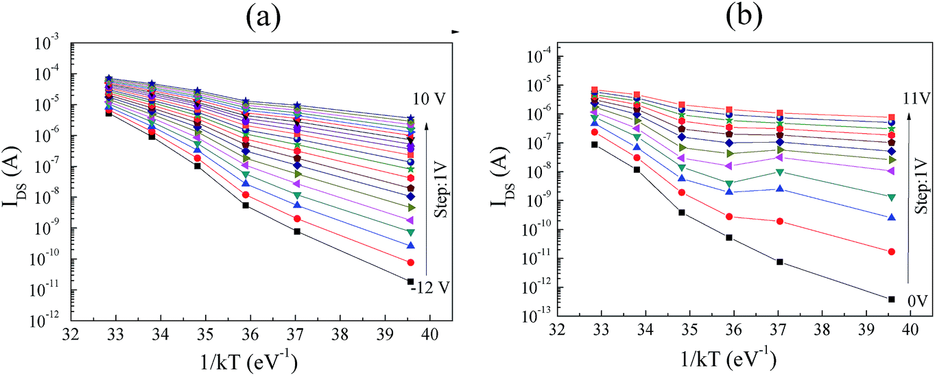
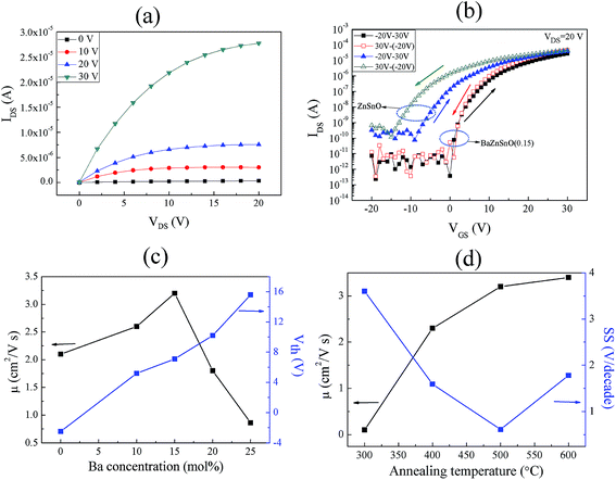
Fig. 4 shows the evolution of the transfer characteristic of ZnSnO-TFT and BaZnSnO-TFT as a function of the temperature. For both devices, the transfer curves are negatively shifted with increasing temperature. As the temperature increases from 293 K to 353 K, Vth of ZnSnO-TFT is shifted by approximately −13.6 V from −2.5 to −16.1 V. However, the corresponding negative Vth shift in BaZnSnO-TFT is relatively small. Vth of BaZnSnO-TFT is shifted by approximately −4.7 V from 7.1 to 2.4 V for BaZnSnO-TFT. BaZnSnO-TFT shows a smaller Vth shift than that of ZnSnO-TFT. At higher temperatures, more electrons can escape from the localized states and contribute to the free carriers, which cause a smaller threshold voltage. The negative Vth shift with increasing temperature may be related to the shift of the Fermi level EF. The shift of EF can be expressed by the variation of the conduction activation energy (Ea). Ea is the energy difference between EF and the edge of the conduction band (EC), which equates to the average energy that a trapped electron escapes from the localized state. In case of general thin film transistors, the temperature dependence of the Vth shift is closely related with the increase in thermally active electrons. It is necessary to investigate the impact of thermally activated process on the change in free electrons. In generally, the generated free electrons in oxide semiconductors are mainly attributed to oxygen vacancies.14 It is reported that thermally activated electrons are exponentially increased with increasing temperature.15 The drain current (IDS) is thermally activated and can be described by:16,17
| | |
IDS = IDS0exp(−Ea/kT)
| (5) |
where
IDS0 is the prefactor,
k is the Boltzmann constant,
T is the temperature,
Ea can be estimated by fitting of temperature-dependent log(
IDS)
versus 1/
T curve as shown in
Fig. 5. It is assumed that thermally activated electron from deep level trap sites into the conduction band move quickly toward the drain electrode under a electrical field. Thus, the rate-limiting process would involve thermal excitation of the trapped charge, and
Ea can be extracted as a function of
VGS in the forbidden bandgap (as shown in
Fig. 6(a)). The maximum
Ea value is obtained to be 1.14 eV at a
VGS of −12 V. For BaZnSnO-TFT, the maximum
Ea value is about 1.09 eV at a
VGS of 0 V, which is similar with the reported value by H. Godo
et al.18 Ea value decreases with increasing
VGS. The decreasing rate of
Ea are estimated to be 0.23 eV V
−1 for BaZnSnO-TFT and 0.11 eV V
−1 for ZnSnO-TFT, indicating that BaZnSnO semiconductor shows a fast moving
EF level of with respective to
VGS. The rate of change in
EF level of with respective to
VGS is inversely proportional to the magnitude of total trap density (
Ntot) including the density of state (DOS) of bulk semiconductor film and interface trap density between active layer and SiO
2 film. The result suggests that BaZnSnO-TFT exhibits a relatively low bulk and interface trap density.
 |
| | Fig. 4 The evolution of the transfer characteristic of ZnSnO-TFT and BaZnSnO (0.15)-TFT as a function of the temperature. | |
 |
| | Fig. 5 Relationship between log(IDS) and 1/T as a function of VGS for (a) ZnSnO-TFT and (b) BaZnSnO (0.15)-TFT. | |
 |
| | Fig. 6 (a) The relation between VGS and Ea. (b) Calculated DOS distribution as a function of Ea. | |
The density of states (DOS) of the BaZnSnO-TFT and ZnSnO-TFT can be extracted from the relationship between Ea and VGS by assuming the current in the active layer distributed uniformly in several hundred angstroms of active layer. The DOS can be calculated using the following equation.19
| |
 | (6) |
where
εi and
di are respectively the permittivity and the thickness of the gate dielectric,
t is the thickness of the active layer, and
q is the electron charge.
Fig. 6(b) shows the relationship between density of state and activation energy of BaZnSnO-TFT and ZnSnO-TFT. For BaZnSnO-TFT, the magnitude of density decreases from 8.9 × 10
18 to 2.8 × 10
17 cm
−3 as the activation energy increases. The calculated DOS distribution is comparable to the reported solution-processed HfInZnO-TFT.
20 The total DOS for BaZnSnO-TFT is obviously smaller than that for ZnSnO-TFT at a specific energy level. The total DOS value at a specific energy level is the summation of bulk trap density and interface state density. Compared with ZnSnO-TFT, BaZnSnO TFTs have a lower density of trap states in the subgap DOS, which leads to superior electrical performance and better temperature stability. Thus, BaZnSnO film could be a useful active layer for high performance thin film transistors.
4. Conclusions
In summary, we have fabricated BaZnSnO-TFT by solution process. Compared to the ZnSnO-TFT, BaZnSnO (0.15)-TFT exhibits a better electrical performance and temperature stability. Extraction of the DOS of transistor using temperature-dependent field effect measurement is used to understand the electrical performance and stability. It is attributed that much smaller oxygen vacancies and DOS distribution compared to the ZnSnO-TFT.
Acknowledgements
The authors would like to acknowledge the financial support given by the Natural Science Foundation of China (51302165, 61274082, 61077013), Shanghai Municipal Education Commission (ZZSD13047), Innovation Fund of shanghai University and China Postdoctoral Science Special Fund (2012T50387).
References
- K. Nomura, H. Ohta, K. Ueda, T. Kamiya, M. Hirano and H. Hosono, Science, 2003, 300, 1269 CrossRef CAS PubMed.
- H. J. Kwang, J. I. Kim, H. Y. Jung, S. Y. Park, R. Choi, K. K. Un, S. H. Cheol, D. Lee, H. Hwang and J. K. Jeong, Appl. Phys. Lett., 2011, 10, 101101 Search PubMed.
- B. D. Ahn, J. S. Park and K. B. Chung, Appl. Phys. Lett., 2014, 105, 163505 CrossRef.
- J. Li, J. H. Zhang, X. W. Ding, W. Q. Zhu, X. Y. Jiang and Z. L. Zhang, Thin Solid Films, 2014, 562, 592 CrossRef CAS.
- K. Nomura, H. Ohta, A. Takagi, T. Kamiya, M. Hirano and H. Hosono, Nature, 2004, 432, 488 CrossRef CAS PubMed.
- C. Wu, X. Li, J. Lu, Z. Ye, J. Zhang, T. Zhou, R. Sun, L. Chen, B. Lu and X. Pan, Appl. Phys. Lett., 2013, 103, 082109 CrossRef.
- P. T. Tue, T. Miyasako, J. Li, H. T. C. Tu, S. Inoue, E. Tokumitsu and T. Shimoda, IEEE Trans. Electron Devices, 2013, 60, 320 CrossRef CAS.
- H. J. Jeon, W. J. Maeng and J. S. Park, Ceram. Int., 2014, 40, 8769 CrossRef CAS.
- G. H. Kim, W. H. Jeong, B. D. Ahn, H. S. Shin, H. J. Kim, H. J. Kim, M. K. Ryu, K. B. Park, J. B. Seon and S. Y. Lee, Appl. Phys. Lett., 2010, 96, 163506 CrossRef.
- B. Y. Su, S. Y. Chu, Y. D. Juang and S. Y. Liu, J. Alloys Compd., 2013, 580, 10 CrossRef CAS.
- T. Jun, K. Song, Y. Jeong, K. Woo, D. Kim, C. Bae and J. Moon, J. Mater. Chem., 2011, 21, 1102 RSC.
- H. C. Wu and C. H. Chien, Appl. Phys. Lett., 2013, 102, 062103 CrossRef.
- J. Li, F. Zhou, H. P. Lin, W. Q. Zhu, J. H. Zhang, X. Y. Jiang and Z. L. Zhang, Vacuum, 2012, 86, 1840 CrossRef CAS.
- K. Hoshino and J. F. Wager, IEEE Electron Device Lett., 2010, 31, 818 CrossRef CAS.
- K. Kim, P. C. Debnath, S. Kim and S. Y. Lee, Appl. Phys. Lett., 2011, 98, 113109 CrossRef.
- C. Chen, K. Abe, H. Kumomi and J. Kanicki, IEEE Trans. Electron Devices, 2009, 56, 1177–1182 CrossRef CAS.
- D. H. Kim, H. K. Jung, D. H. Kim and S. Y. Lee, Appl. Phys. Lett., 2011, 99, 162101 CrossRef.
- H. Godo, D. Kawae, S. Yoshitomi, T. Sasaki, S. Ito, H. Ohara, H. Kishida, M. Takahashi, A. Miyanaga and S. Yamazaki, Jpn. J. Appl. Phys., 2010, 49, 03CB04 CrossRef.
- Y. H. Tai, H. L. Chiu and L. S. Chou, J. Electrochem. Soc., 2012, 159, J200 CrossRef CAS.
- W. H. Jeong, G. H. Kim, H. S. Shin, B. D. Ahn, H. J. Kim, M. K. Ryu, K. B. Park, J. B. Seon and S. Y. Lee, Appl. Phys. Lett., 2010, 96, 093503 CrossRef.
|
| This journal is © The Royal Society of Chemistry 2015 |
Click here to see how this site uses Cookies. View our privacy policy here.