 Open Access Article
 This Open Access Article is licensed under a
 Creative Commons Attribution 3.0 Unported Licence
Concluding remarks: emerging inorganic materials in thin-film photovoltaics
Aron
Walsh

Department of Materials, Imperial College London, London SW7 2AZ, UK. E-mail: a.walsh@imperial.ac.uk
First published on 18th August 2022
Abstract
A personal perspective is given on the major results, themes and trends from the Faraday Discussion on emerging materials for solar energy technologies. This covers research progress into adamantine semiconductors, the narrowing divide between materials modelling and measurements of solar cells, as well as the control of defects in novel absorber materials that include Cu2ZnSnS4, Zn3P2, Se, GeSe, Sb2Se3 and BaZrS3. This paper is adapted from a transcript of the closing lecture.
1. Introduction
It is hard to believe that this was only a 48 hours meeting because each session has been so intense. Both in terms of the volume of results reported and the depth of the discussion, the event has been a little overwhelming. Perhaps, I am just out of practice due to the global pandemic. I was given the difficult task to sum up the major themes that emerged in this meeting. Of course, this is from my perspective, so I will also share my opinions on some of the important issues raised.On the train from London to Bath, I collected the abstracts from the event programme and generated a word cloud (see Fig. 1) to have a feeling for what I could expect. In the text, you can see many of the points that have been discussed. Of course, the main focus is solar energy. There is coverage of kesterites, some mention of perovskites, and an emphasis on efficiency, performance and stability. It reflects what we have been actively discussing.
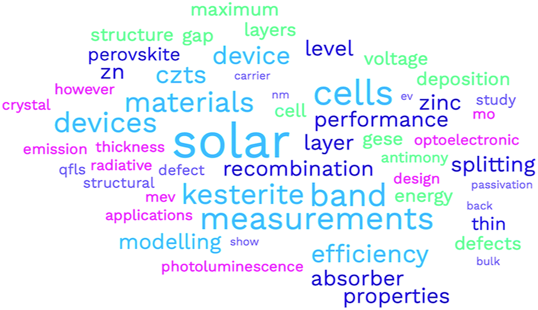 | ||
| Fig. 1 A word cloud generated from the abstracts of papers presented at the Faraday Discussion meeting on emerging materials for solar energy technologies. | ||
To begin, the topic of this Faraday Discussion is emerging photovoltaic (PV) materials. We have heard that many of the systems studied have a long history. Some for many decades. So by “emerging”, we don’t necessarily mean that these are new materials or new technologies. One way to classify them is according to their performance with respect to the detailed balance limit (see Fig. 2). In most cases, we’ve heard about materials that fall in the bottom 50%. Materials that don’t yet realise half of their potential. Following this definition, we are making life difficult for ourselves. We’re not using the highest performing materials and looking for incremental improvements. We’re choosing technologies that have potential, but fundamental science needs to be completed to understand the current bottlenecks and to engineer higher performance devices. It is a difficult topic by definition. But it has been inspiring to see the progress being made and the exciting ideas that people shared over the past few days.
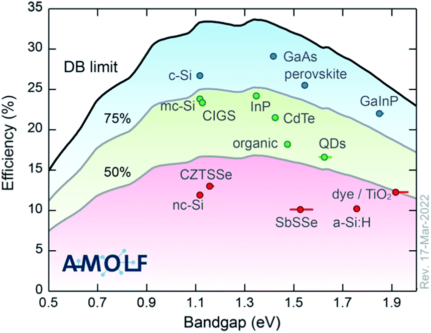 | ||
| Fig. 2 The champion light-to-electricity conversion efficiencies for a range of photovoltaic technologies with respect to the detailed balance limit. The image is reproduced with permission from https://www.lmpv.nl/db/ and an earlier version was published in ref. 1. | ||
2. Beyond chalcopyrites
Session one takes us all the way back to Monday for “beyond chalcopyrites” with a series of talks related to progress in kesterite (A2BCX4) based solar cells. I was reminded a couple of weeks ago, at a See FuturePV conference talk by Susan Schorr, about the work of Brian Pamplin. Pamplin was a faculty member in the Department of Physics here at the University of Bath. He explored the chemical space for forming multi-component tetrahedral semiconductors from the 1960s.2 The science of standard III–V and II–VI tetrahedral semiconductors was well developed. He thought about going to ternary, quaternary, even quintenary systems. And in some cases doing back-of-the-envelope calculations to assess which materials should exist and then actually attempting to grow them in the lab. Pamplin had an important series of papers and this image (Fig. 3) is from a 1980 review.3 He terms this the adamantine family, referring to the mythical unbreakable crystal. Generally, adamantine refers to diamond based structures, which are densely packed and quite hard to break. Stability is of course one of the reasons why this community is so interested in such chalcogenide systems.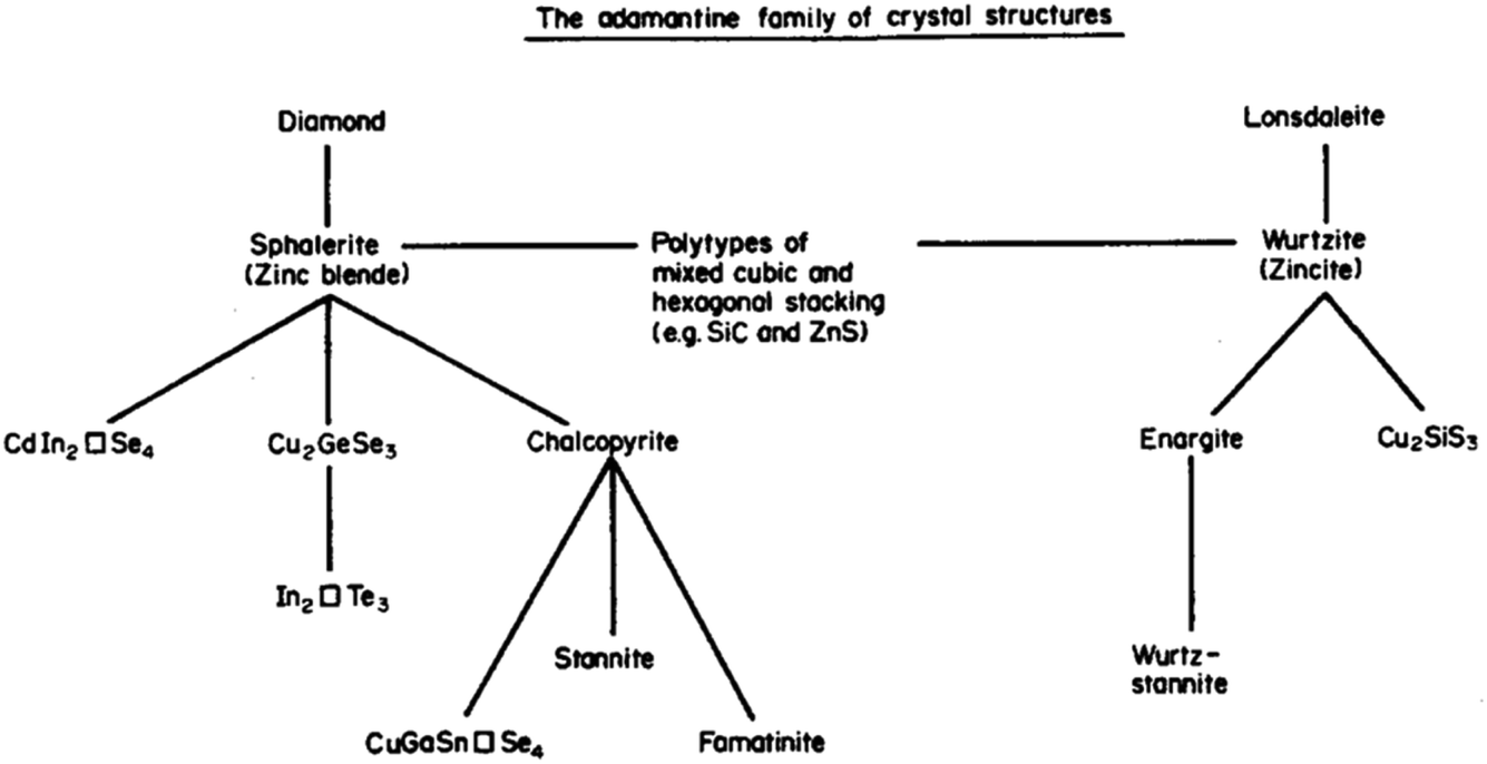 | ||
| Fig. 3 A map of the relationship between adamantine crystal structures adapted with permission from ref. 3. | ||
Pamplin considered building blocks based on face-centred cubic and hexagonal close packing. He thought of stoichiometric combinations, as well as ordered vacancy systems. When you follow the two strands for binary compounds, you have zinc blende versus wurtzite, with ternary and quaternary equivalents, for example, stannite and wurtz-stannite (these are closely related to the kesterite and wurtz-kesterite structures4). For certain compositions, such as Cu2CdSiS4, the hexagonal stacking sequences are favoured.5 In fact, when you look at high-resolution microscopy over large areas, often the competition between AB and ABC close-packing leads to stacking faults, a type of planar defect.6 We once performed some simulations of this phenomenon,7 but I recall that their connection to photovoltaic efficiency is still not well understood. It is nice to think that decades ago at this location, someone was concerned with similar problems to us now.
Actually a lot of my post-doctoral work was inspired by the pioneering work of Pamplin and others working in a similar direction such as Colin Goodman.8 At the time I was working at the National Renewable Energy Laboratory and had access to some quite large Department of Energy computers. We decided to map out this crystal space systematically, looking at many chemistries of going from the elemental to quaternary systems in terms of the structures that emerge and also the property trends.9 This was largely the PhD work of my collaborator Shiyou Chen. It is a field that I have enjoyed working in since then. This type of materials workflow is attractive because you can control the complexity, adding one more component when you go down a series. But there is an associated cost. In each session of this meeting, we have heard about defects in crystals. In quaternary systems, the situation becomes incredibly difficult because so many point defects (vacancies, interstitials, anti-sites), complexes that form between neighbouring sites, and extended defects can form in tandem.10
In Cu2ZnSnS4, Cu–Zn disorder is an issue, but unlikely to be the bottleneck for photovoltaic performance.11 It is really the Sn-related defects that act as killer centres. They result in deep levels that are the strongest traps for recombining electrons and holes.12 The challenge here is that often the Sn-related defects are hidden beneath the Cu–Zn disorder. Because you have such high levels of cation site mixing, it’s very difficult to see the small changes. Even if some of these defects are present in parts per million, they could still be responsible for large voltage deficits. That’s one of the challenges in trying to get to grips with these systems. From the kesterite presentations that we heard, and the community feeling in general, a big open question remains: is there a future for kesterites? What we have on our side is materials engineering. So I think there is always hope. But we need a breakthrough in this field such as a new processing step that suddenly activates the photovoltaic performance of Cu2ZnSnS4 absorbers to approach 20% light-to-electricity conversion efficiency.
3. Characterisation of solar absorbers
On the second morning there was an interesting session on materials’ characterisation. We heard about the state of the art in photoluminescence analysis through to time-resolved behaviour that shed light on the carrier lifetimes and recombination pathways in some interesting systems. I have a particular bias because I work in theory and simulation of materials, and one of my goals is to bridge between modelling and measurements. So paying attention to the latest experimental techniques, the progress in spatial and temporal resolution, and seeing how we can bring atomistic modelling closer to really what can be measured. I would like to raise a couple of relevant points that are of interest for emerging PV.In the past, if you’re concerned about materials’ properties such as electrical conductivity, chemical stability, photogenerated carrier lifetimes, it would be quite common to use a method like density functional theory (DFT) to make predictions. You calculate the electronic band structure to get an effective mass, then wave your hands and say this should be a good p-type conductor or that should be a good n-type conductor. But now we can actually calculate carrier mobilities, by estimating the electron and hole scattering rates, which don’t always follow the underlying effective masses.13 You might have a system that has low lying vibrational states that scatter strongly and limit mobility at room temperature. Then for stability fields and materials processing, the standard practice was to work with athermal internal energies from DFT. But when you heat materials, the thermodynamic balance can change. You may have a phase that would be stable at 0 K, but at room temperature is no longer accessible. It’s now possible to go from internal energies to free energies and so include temperature and pressure dependence in phase diagrams. That’s becoming increasingly standard and we previously developed models for kesterites.14 The third point, which we heard about this morning from Seán Kavanagh (https://doi.org/10.1039/D2FD00043A), is defects. In the past it was standard practice to calculate defect levels, a series of charge state transitions between the valence and conduction bands of a host crystal. These allowed for qualitative comparison with a range of optical and electronic probes but there was no direct connection for unambiguous assignments. We heard that we are now closer to calculating the spectroscopic features of particular defects. A move in that direction is the calculation of carrier capture coefficients,15 considering the interaction of defects with electron and hole and carriers, which has been a focus for my research group over the past few years. A talented researcher Sunghyun Kim led the development of the CarrierCapture package16 and we have applied it to a range of cases from Cu2ZnSnS4 (ref. 17) to GaAs.18
This transition to a higher complexity in the modelling does not come for free. These are not calculations that you can run on your laptop. They often use large-scale national supercomputing resources. The website Top500 (https://www.top500.org) provides a ranking of the fastest public supercomputers in the world. And now in the U.S., they’ve launched a supercomputer that has 8.7 million cores. One computer with 8.7 million processing units. That’s amazing! There are now several public systems in the world with over 1 million cores. But you also have to pay attention to the power consumption. The top entry requires 21![[thin space (1/6-em)]](https://www.rsc.org/images/entities/char_2009.gif) 000 kW to operate. The equivalent of an old generation coal power plant just running that one computer. One active question is the sustainability of computational research. Should we do everything brute force at the highest level of theory possible, or should we try to be smarter in what we do and how we do it? That’s the subject of ongoing debate and developments. We have methods that are very accurate, but it’s not feasible to run them out for every possible material because you’re just wasting so much energy and generating tons of CO2 along the way.
000 kW to operate. The equivalent of an old generation coal power plant just running that one computer. One active question is the sustainability of computational research. Should we do everything brute force at the highest level of theory possible, or should we try to be smarter in what we do and how we do it? That’s the subject of ongoing debate and developments. We have methods that are very accurate, but it’s not feasible to run them out for every possible material because you’re just wasting so much energy and generating tons of CO2 along the way.
4. Novel semiconductors
In session three we tackled novel materials covering everything from Zn3P2 to GeSe. One point, when you look at a lot these unconventional emerging materials for photovoltaics, is that they generally have crystal structures that are anisotropic.19 This is different to cubic semiconductors that are standard in PV such as Si, CdTe and GaAs. Even if chalcopyrites or kesterites formally have tetragonal structures, they still feature tetrahedral bonding networks in three dimensions. So the level of anisotropy is very weak. In newer systems like Sb2S3, there are rods, chains, sheets or more complex connectivity, which of course introduces the challenge of crystal orientation (Fig. 4a). For example, do we understand which orientation gives the best photovoltaic response and how you could reproducibly scale up the fabrication? For this reason, anisotropy has been on my mind. I won’t add too much because Xinwei Wang introduced this nicely in her flash presentation (see the list of posters in this volume), but the antimony chalcogenides are a curious case because nearly every report refers to them as one dimensional structures. Definitely, when you look at the unit cell you can see rods that form essentially one dimensional blocks. And in many cases that’s the preferential growth direction, which leads to needle-like crystals. But there is a wide distribution of Sb–X bond lengths distribution (Fig. 4b). My question to Xinwei: what is the electronic dimensionality? To cut a long story short, we found that the dimensionality depends on the property you’re interested in. So it might be that you have particular structural dimensionality, but then the bond strength, dielectric functions, effective masses each have their own anisotropy.20 But one point we thought would be of direct relevance to this community is the carrier mobility, which shows that the conduction pathways in Sb2X3 can be classified as 2D or 3D depending on the composition and carrier type.21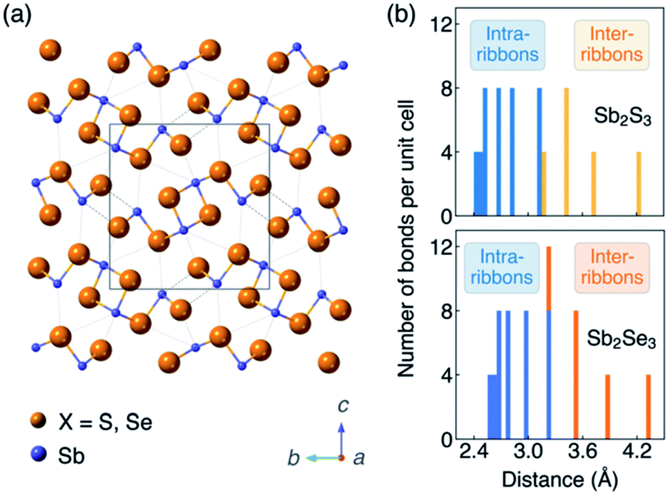 | ||
| Fig. 4 (a) Crystal structure (Pnma space group) and (b) histogram of Sb–X distances of the photovoltaic absorber materials Sb2S3 and Sb2Se3. The figure is reproduced from ref. 20 under a Creative Commons CC-BY license. | ||
5. Design principles and defect tolerance
On the final morning we heard about emerging design principles with an emphasis on the control of defects ranging from dilute imperfections to high-concentrations that aggregate to form ordered defect complexes. The last point I want to touch upon is defect tolerance, because this is a topic discussed throughout this meeting. One difficulty is that defect tolerance is often used as an umbrella term for several types of behaviour. There are many claims of defect tolerant materials in the literature. Some refer to high photovoltaic efficiency despite high concentrations of defects. Others refer to a material where there appears that no deep traps are formed. It could be a crystal that’s straightforward to dope p-type and n-type without charge compensation. In the halide perovskite community, it is often linked to PV performance that is insensitive to growth conditions or even stoichiometry. Ultimately, we want PV materials that can perform well no matter how poorly you make them or treat them. It is asking for a lot.A question debated earlier is how we can emulate the defect tolerance of metal halide perovskites in other materials. I have a particular opinion that not everybody would share, but I would say the number one reason for perovskites being so tolerant is simply dielectric screening. This property is related both to the perovskite structural flexibility and the chemical softness of the constituent ions, which give rise to large Born effective charges and in turn a sizable ionic contribution to the dielectric response. Why is this relevant for solar cells you ask? In the screening of electrostatic interactions, whether it be electron–hole separation or electron-charged defect scattering, it is beneficial to have a large dielectric constant.22 Many relevant interaction terms depend on the square of the dielectric constant. As halide perovskites generally have large dielectric constants, they have small carrier capture cross-sections. Of course there are other factors to consider, one of which is lattice thermal conductivity. Non-radiative losses are facilitated by heating and if the host crystal is a thermal insulator then any recombination cycle will be supressed. I don’t believe this has been well explored for photovoltaics except for the slowing of hot carrier cooling in nanostructured materials and quantum dot solar cells.
In conclusion, I’ll restate several opportunities. For emerging materials, David Mitzi outlined the balance between simplicity and tuneability in his opening lecture (https://doi.org/10.1039/D2FD00132B). We heard about Se in the final morning’s session. In principle, you can’t get simpler than one element but even Se has many structural forms to control. Perhaps simplicity is not just the number of elements and we need to develop better structure and property features. The need for new electrical contacts for emerging technologies was highlighted. CdS may have a refined deposition procedure in this community, but it is not optimal in terms of performance and also for its composition. What has been used a lot in the organic photovoltaic community is modification layers. For example, while TiO2 may not have an appropriate conduction band for your technologies, an ultra-thin molecular or polymeric dipole layer could alter the contact behaviour with shifts on the order of eV possible. It is a trick that could be useful here, instead of going directly to alloys and trying to balance band gap and resistivity changes. Finally, I will echo Thomas Unold’s call for better use and sharing of data concerning both PV materials and devices (https://doi.org/10.1039/D2FD00085G). So much information gets hidden in the literature that you can’t access or reproduce. I look forward to a future where a photovoltaic information file (.pif) becomes standard with each new publication.
Our understanding of emerging photovoltaic materials continues to grow and I hope that we can learn from past experiences to accelerate the development of the exciting technologies that have been covered at this event.
References
- A. Polman, M. Knight, E. C. Garnett, B. Ehrler and W. C. Sinke, Science, 2016, 352, 307 CrossRef CAS PubMed.
- B. R. Pamplin, J. Phys. Chem. Solids, 1964, 25, 675–684 CrossRef CAS.
- B. R. Pamplin, Prog. Cryst. Growth Charact., 1980, 3, 179–192 CrossRef CAS.
- S. Schorr, H.-J. Hoebler and M. Tovar, Eur. J. Mineral., 2007, 19, 65–73 CrossRef CAS.
- S. Chen, A. Walsh, Y. Luo, J.-H. Yang, X. G. Gong and S.-H. Wei, Phys. Rev. B: Condens. Matter Mater. Phys., 2010, 82, 195203 CrossRef.
- N. Kattan, B. Hou, D. J. Fermín and D. Cherns, Appl. Mater. Today, 2015, 1, 52–59 CrossRef.
- J.-S. Park, S. Kim and A. Walsh, Phys. Rev. Mater., 2018, 2, 014602 CrossRef CAS.
- C. H. L. Goodman, J. Phys. Chem. Solids, 1958, 6, 305–314 CrossRef.
- S. Chen, X. G. Gong, A. Walsh and S.-H. Wei, Phys. Rev. B: Condens. Matter Mater. Phys., 2009, 79, 165211 CrossRef.
- S. Chen, A. Walsh, X.-G. Gong and S.-H. Wei, Adv. Mater., 2013, 25, 1522–1539 CrossRef CAS PubMed.
- S. Bourdais, C. Choné, B. Delatouche, A. Jacob, G. Larramona, C. Moisan, A. Lafond, F. Donatini, G. Rey, S. Siebentritt, A. Walsh and G. Dennler, Adv. Energy Mater., 2016, 6, 1502276 CrossRef.
- S. Kim, J.-S. Park, S. N. Hood and A. Walsh, J. Mater. Chem. A, 2019, 7, 2686–2693 RSC.
- A. M. Ganose, J. Park, A. Faghaninia, R. Woods-Robinson, K. A. Persson and A. Jain, Nat. Commun., 2021, 12, 2222 CrossRef CAS.
- A. J. Jackson and A. Walsh, J. Mater. Chem. A, 2014, 2, 7829–7836 RSC.
- A. M. Stoneham, Rep. Prog. Phys., 1981, 44, 1251 CrossRef.
- S. Kim, S. N. Hood, P. van Gerwen, L. D. Whalley and A. Walsh, J. Open Source Softw., 2020, 5, 2102 CrossRef.
- S. Kim, J. A. Márquez, T. Unold and A. Walsh, Energy Environ. Sci., 2020, 13, 1481–1491 RSC.
- S. Kim, S. N. Hood and A. Walsh, Phys. Rev. B, 2019, 100, 041202 CrossRef CAS.
- V. Steinmann, R. E. Brandt and T. Buonassisi, Nat. Photonics, 2015, 9, 355–357 CrossRef CAS.
- X. Wang, Z. Li, S. R. Kavanagh, A. M. Ganose and A. Walsh, Phys. Chem. Chem. Phys., 2022, 24, 7195–7202 RSC.
- X. Wang, A. M. Ganose, S. R. Kavanagh and A. Walsh, ACS Energy Lett., 2022, 7, 2954–2960 CrossRef CAS.
- R. E. Brandt, V. Stevanović, D. S. Ginley and T. Buonassisi, MRS Commun., 2015, 5, 265–275 CrossRef CAS.
| This journal is © The Royal Society of Chemistry 2022 |