 Open Access Article
 This Open Access Article is licensed under a Creative Commons Attribution-Non Commercial 3.0 Unported Licence
A post-deposition annealing approach for organic residue control in TiO2 and its impact on Sb2Se3/TiO2 device performance
Mykhailo
Koltsov
*a,
Robert
Krautmann
a,
Atanas
Katerski
a,
Natalia
Maticiuc
 b,
Malle
Krunks
a,
Ilona
Oja Acik
a and
Nicolae
Spalatu
*a
b,
Malle
Krunks
a,
Ilona
Oja Acik
a and
Nicolae
Spalatu
*a
aDepartment of Materials and Environmental Technology, Tallinn University of Technology, Ehitajate tee 5, 12616 Tallinn, Estonia. E-mail: nicolae.spalatu@taltech.ee
bCompetence Centre Photovoltaics Berlin (PVcomB), Helmholtz-Zentrum Berlin für Materialen und Energie (HZB), Schwarzschildstraße 3, 12489 Berlin, Germany
First published on 21st April 2022
Abstract
We report a systematic investigation on the influence of two-step post-deposition treatments (PDTs) on TiO2 buffer layers deposited by ultrasonic spray pyrolysis (USP) for emerging Sb2Se3 photovoltaics. Air annealing is a typical method for recrystallizing chemically deposited TiO2 films. However, organic residues (such as carbon species) from a precursor solution based on titanium tetraisopropoxide and acetylacetone may still remain on the TiO2 surface, therefore requiring an additional annealing step. We demonstrate that vacuum annealing can be a suitable technological approach to decrease the concentration of carbon species in TiO2 films. Vacuum annealing was performed at temperatures at 160–450 °C prior to the 450 °C air annealing step. It was found that vacuum annealing at 160 °C followed by subsequent air annealing led to better device performance. This was explained by achieving an optimal balance between the removal of carbon content during vacuum annealing and the active recrystallization of TiO2 during air annealing. The decrease of carbon concentration by employing the two-step approach was supported by changes in the lattice parameters of TiO2 and proven by X-ray photoelectron spectroscopy (XPS). The given study provides experimental evidence on how nanoscale carbon species in the TiO2 heterojunction partner layer of a Sb2Se3 solar cell can affect the device’s performance. By this approach, we generate complementary insights on how the quality of the main interface has an impact and can take a key role despite the optimized Sb2Se3 grain structure and orientation.
Introduction
The field of thin film photovoltaics (PV) is booming at the moment as it is seeing remarkably fast progress in the development and optimization of new emerging semiconductor absorber materials, such as thin sulfides,1 chalcostibites,2 chalcogenide perovskites,3 nitrides,4 and antimony chalcogenides.5,6 These materials have attracted intensive thin film PV research of late because of the high abundance of their constituent elements in the Earth’s crust and the non-toxicity of the chemical elements, which are combined with highly demanded material qualities, such as defect tolerance6 and high chemical stability. Among these materials, Sb-chalcogenides, e.g., Sb2Se3, Sb2S3, and Sb2(S,Se)3, have demonstrated great potential with a nascent track record of performance development. Sb2Se3 and Sb2S3 are both single-phase binary compounds with quasi-one-dimensional crystal structures, absorption coefficients of >104 cm−1 (for energies above 1.5 eV)7,8 and band gap energies of ∼1.2 eV and ∼1.7 eV,9,10 respectively. Such optoelectronic properties are excellent for developing efficient thin film solar cell devices.Despite a paucity of research, PV devices based on antimony chalcogenides have already reached cell power conversion efficiencies (PCEs) of around 10%.11 As for Sb2Se3, the absorber material in the focus of the current study, absorbers deposited by close-spaced sublimation12,13 and vapor transport14 deposition techniques have produced devices with record PCEs ranging between 7–9%. Despite these achievements, there are several challenges that need to be overcome to harness the full potential of Sb2Se3 PV devices. Critical limitations include finding an optimal device structure,15 optimization of Sb2Se3 growth,6,12,13 identification of suitable heterojunction partner layers,9,15,16 and development of post-deposition treatments and doping strategies.17,18 Most of the R&D efforts in recent years have been focused on optimizing Sb2Se3 growth, in conjunction with a CdS heterojunction buffer layer, an established partner layer in CdTe,19 CIGS,20 and CZTS solar cells.21 While the CdS buffer layer (Eg ∼ 2.5 eV)22 has been the preferred choice for a majority of research groups,9,14,23 and has shown favorable band alignment with the Sb2Se3 absorber,15 TiO2 buffer layers (Eg = 2.8–3.3 eV)24 have emerged as suitable and more stable alternatives to CdS buffer layers. Namely, chemical intermixing at the interface between CdS and Sb2Se3 has been reported in superstrate Sb2Se3/CdS PV devices, causing the formation of an interface layer, which acts like an electrostatic barrier that obstructs charge transfer and collection.13 As for TiO2 synthesis, spin coating (SC)13 and ultrasonic spray pyrolysis (USP)25 are common deposition techniques, especially for superstrate Sb2Se3/TiO2 PV devices. The best superstrate Sb2Se3/TiO2 solar cells have thus far demonstrated PCEs between 5–8%.5,12
Despite these promising results, there is ongoing research into various aspects of how the heterojunction between TiO2 and Sb2Se3 can be improved. Since Sb2Se3/TiO2 PV devices suffer from substantial VOC deficits, developing a strategy for Sb2Se3/TiO2 interface engineering is of extreme importance for giving Sb2Se3/TiO2 solar cells a further boost. One of the aspects in the Sb2Se3/TiO2 interface engineering entails post-deposition treatment of the TiO2 films after the films have been deposited by either UPS or SC chemical methods. Usually, such a treatment implies thermal annealing in air at 450–500 °C for 20–30 min,10 with the main purpose of improving the crystallinity of the TiO2 films. It is mostly accepted that for chemically deposited TiO2 layers, air annealing at elevated temperatures causes residual organic components, which are inevitably present in the precursor solution, to be easily removed as a result of a pyrolysis process. However, in our recent study, we noticed that the pyrolysis process in the presence of air at high temperatures might not be enough to purge the TiO2 films of organic residuals, and to some extent, organic residuals may remain on the TiO2 surface and could degrade the quality of the Sb2Se3/TiO2 interface and curtail the performance of the device.12 Hence, this finding served as a hypothesis, forming the basis of the subsequent study with the focus of systematically investigating the effects of different annealing procedures over a wide range of temperatures on the properties of the TiO2 films and the performance of Sb2Se3/TiO2 solar cells. With this approach, we aimed to screen the evolution of organic residues at the surface of USP-deposited TiO2 films, gain an understanding of the kinetics of a vacuum annealing process for removing these organic residuals, and assess the overall impact of annealing on Sb2Se3/TiO2 solar cell performance.
Experimental
Fabrication of superstrate configuration glass/FTO/TiO2/Sb2Se3/Au thin film solar cells
The solar cells were fabricated according to the superstrate configuration. FTO-coated 2.3 mm thick glass with a surface resistivity of 7 Ω sq−1 (provided by Sigma-Aldrich) was used as a substrate. USP TiO2 films were deposited atop FTO at 340 °C using a precursor solution of a 1![[thin space (1/6-em)]](https://www.rsc.org/images/entities/char_2009.gif) :4 ratio of titanium(IV) isopropoxide (TTIP) and acetylacetone (AcacH). The USP deposition was set in a way to keep a constant controllable TiO2 thickness of 80–90 nm. In the next step, the TiO2 films were divided into two sets and subjected to three different annealing procedures, described in the section below. After the annealing of TiO2, a 1.3–1.5 μm thick Sb2Se3 absorber layer was deposited at 460 °C by CSS, following a previously described procedure.26 5 N granular Sb2Se3 (Sigma-Aldrich) was used as the source material for the absorber deposition. To complete the solar cell, an Au back contact was deposited via thermal evaporation.
:4 ratio of titanium(IV) isopropoxide (TTIP) and acetylacetone (AcacH). The USP deposition was set in a way to keep a constant controllable TiO2 thickness of 80–90 nm. In the next step, the TiO2 films were divided into two sets and subjected to three different annealing procedures, described in the section below. After the annealing of TiO2, a 1.3–1.5 μm thick Sb2Se3 absorber layer was deposited at 460 °C by CSS, following a previously described procedure.26 5 N granular Sb2Se3 (Sigma-Aldrich) was used as the source material for the absorber deposition. To complete the solar cell, an Au back contact was deposited via thermal evaporation.
Post deposition annealing of USP TiO2 films
After the deposition, the TiO2 sets underwent three annealing procedures: (I) vacuum annealing only (labeled as “Vac”), (II) vacuum and subsequent air annealing (labeled as “Vac+Air”), and (III) air annealing only (labeled as “Air”); vacuum annealing of the USP TiO2 films was carried out in a closed process tube with a diameter of 55 mm and a volume of 1500 mL. For this procedure, the process tube containing the samples was evacuated at room temperature (RT) and then introduced into a cylindrical furnace set at RT, to allow a slow thermal annealing process. The annealing temperature was varied in the 160–450 °C range in steps of ΔT = 50 °C, and the annealing time was fixed at 60 min. The vacuum level in the process tube was maintained at ∼10−5 mbar, using a turbomolecular vacuum pump in a dynamic regime. Air annealing of the USP TiO2 films was carried out in a pre-heated open process tube at 450 °C. The annealing time was fixed at 30 min, after which the tube was taken out from the furnace for rapid cooling at room temperature.Material and device characterization
X-ray diffraction (XRD) and scanning electron microscopy (SEM) were used to analyze the structural and morphological properties of the samples. XRD characterization was carried out on a Rigaku Ultima IV diffractometer with Cu Kα radiation (λ = 1.54 Å, 40 kV, 40 mA). Rigaku PDXL software was used to analyze the XRD data. The following data cards were used: JCPDS 01-089-0821 for Sb2Se3, JCPDS 00-021-1272 for TiO2 and JCPDS 01-077-0452 for FTO (SnO2). A Zeiss HR-SEM MERLIN SEM with the GEMINI II column was used for the top and cross-sectional views of the structures. The XPS spectra were measured with a standard XPS laboratory system based on a nonmonochromatic X-ray source from SPECS with a Mg anode, providing an excitation energy of 1253.6 eV.27 All XPS spectra were measured at room temperature at a pressure of 5 × 10⁻⁶ Pa. The energy analyzer was calibrated by fixing the C 1s core level binding energy at 285.0 eV. AUTOLAB PGSTAT 30 and an Oriel class A solar simulator 91159A (100 mW cm−2, AM1.5) were used for J–V characteristic measurements. In the EQE measurements, a 300 W xenon lamp and an SPM-2 Carl Zeiss-Jena monochromator were used at 30 Hz.Results and discussion
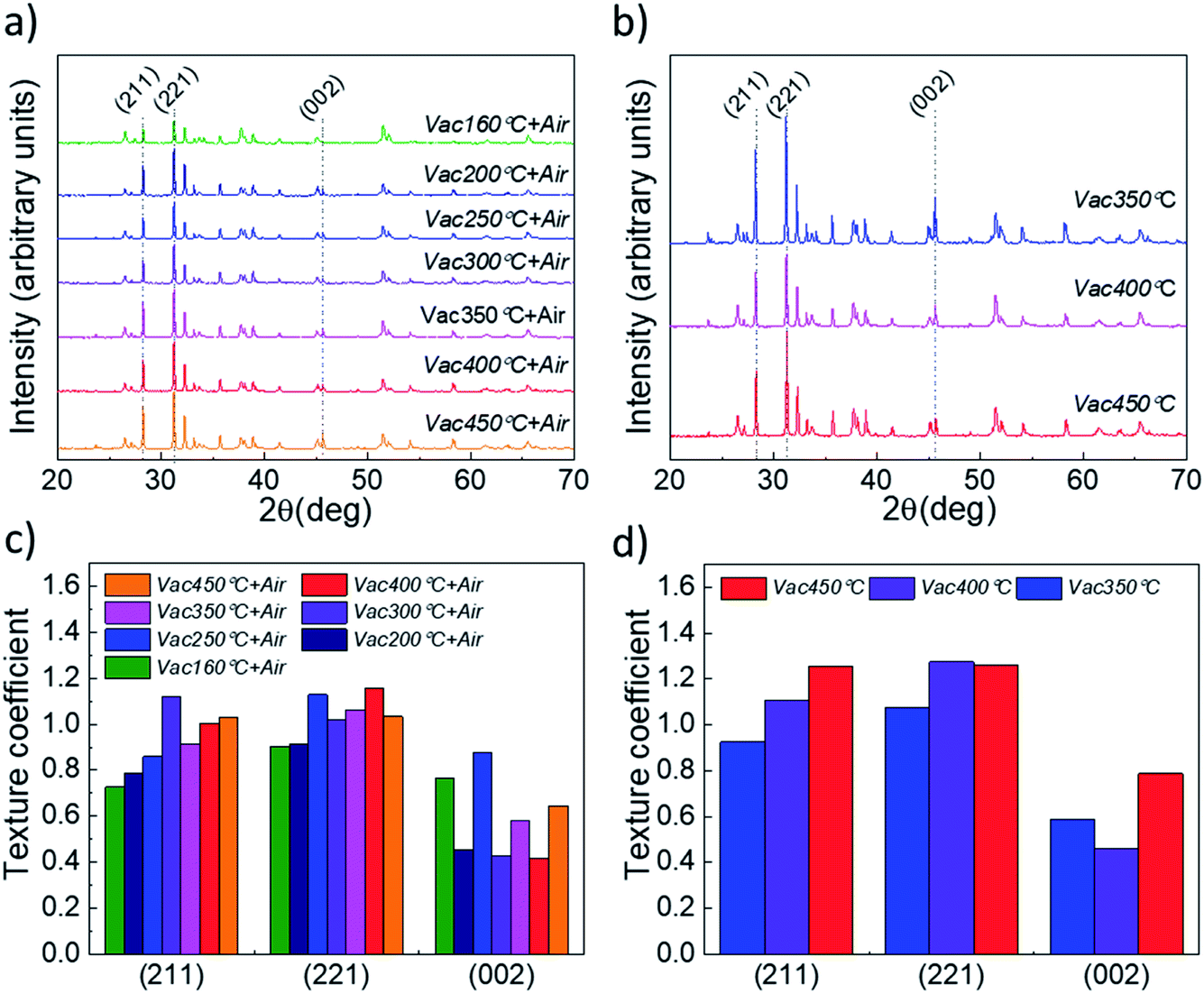
XRD and SEM techniques were used to analyze the structural properties of the as-deposited and annealed TiO2 films. Fig. 1a and b show the XRD patterns of the TiO2 films which underwent different annealing steps. It is observed that for the as-deposited TiO2 film, the diffractogram does not show clearly distinguishable peaks related to the TiO2 crystal structure, indicating that the layers contain a large amount of the amorphous phase. The amorphous phase is kept present in both the Vac+Air and Vac 160–250 °C annealing steps. For Vac+Air and Vac annealing in the range of 300–450 °C, all the TiO2 films showed an anatase crystal structure (PDF: JCPDS 00-021-1272), with characteristic (101) and (200) peaks at 25.28° and 48.05°, respectively . These peaks are characteristic of anatase TiO2 and have been previously reported for USP-deposited TiO2 films.28 To understand the effect of annealing conditions on the structural properties of TiO2 layers, we further analyzed the changes in the crystallite sizes (Fig. 2d, e). As an overall trend, the crystallite size increases with the increase of the Vac+Air and Vac annealing temperatures. For the Vac+Air treatment (Fig. 2d), crystallites were ≈30 nm at low-T (160–250 °C) annealing and ≈50 nm at high-T (300–450 °C) annealing. In the case of the Vac annealing, the trend in crystallite size was slightly sharper, with ≈20 nm size at low-T (160–250 °C) and ≈60 nm large crystallites after annealing at 450 °C (Fig. 2e).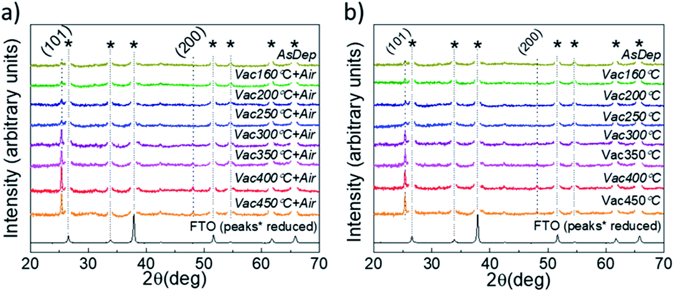 | ||
| Fig. 1 XRD patterns of TiO2 thin films (showing the characteristic (101) and (200) peaks of anatase TiO2) deposited by USP onto FTO/glass substrates, before and after annealing procedures. (a) Vacuum annealing at the temperature range of 160–450 °C for 60 min, and subsequent air treatment at 450 °C for 30 min (labelled as VacT°+Air). (b) Vacuum annealing at 160–450 °C for 60 min (labeled as VacT°). For a better clarity of the diffractograms, the strong peak reflections related to FTO underlayer (marked with star symbols) were artificially reduced. | ||
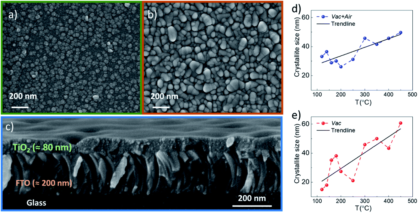 | ||
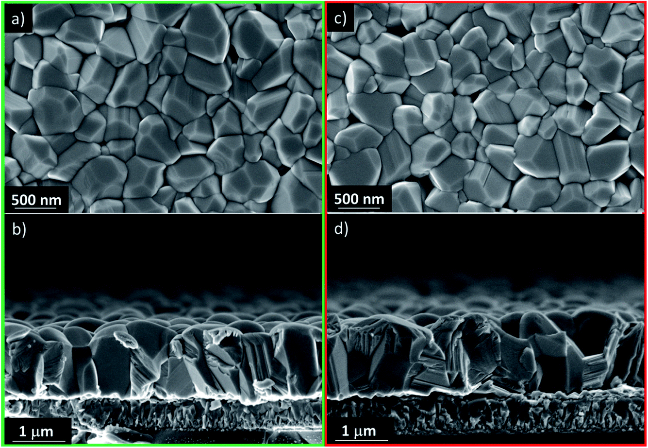
| Fig. 2 (a and b) Top view SEM images of USP-deposited TiO2 after a 160 °C vacuum annealing step (Vac) and after 160 °C vacuum and subsequently 450 °C air annealing steps (Vac+Air), respectively. (c) Cross-sectional view of the TiO2 layer after 160 °C vacuum and subsequently 450 °C air annealing steps (Vac+Air). (d and e) Evolution of the crystallite size of vacuum and subsequently air annealed (labeled as Vac+Air) and vacuum annealed only (labeled as Vac) TiO2 films. | ||
Fig. 2a and b show the top-view SEM images of the TiO2 samples before and after vacuum annealing at 160 °C and subsequent 450 °C air treatment, respectively. The cross-sectional view of the 160 °C vacuum annealed and 450 °C subsequent air treated TiO2 layer is shown in Fig. 2c. As can be seen in Fig. 2a, the amorphous TiO2 film consists of small grains and has quite a homogeneous distribution. After annealing, the films are more compact with well-sintered grains (Fig. 2b) and the thickness is reasonably uniform (Fig. 2c). It is important to note that the TiO2 films kept the same morphology (shown in Fig. 2b) independent of the Vac+Air, Vac, or Air annealing at 450 °C. It is also worth mentioning that from the UV-Vis measurements (Tauc plots, not shown), the band gap value of TiO2 was determined to be Eg ∼3.3 eV and no changes in this value have been observed, independent of either Vac+Air, Vac, or air annealing at 450 °C.
Based on the above XRD and SEM results, it can be concluded that there were no noticeable differences in the properties of TiO2 films when annealed with different Vac+Air, Vac, or Air conditions. A systematic increasing trend in the crystallite size with the increase of annealing temperature was expected, however looking from the perspective of the organic impurity incorporation into the lattice of TiO2 films, the evolution in the lattice parameters of the annealed films was analyzed. The lattice parameters of anatase TiO2 correspond to tetragonal crystal lattice with a = b ≠ c and the values for the Vac160 °C annealed films were between a = b ∼ 3.68–3.75 and c ∼ 9.50–9.52 Å. A small but systematic gradual decrease of the lattice parameters along all the a, b and c axes, from a = b ∼ 3.75, c = 9.51 Å in the Vac160°C annealed films to a = b ∼ 3.80, c = 9.55 Å in the Vac450°C treated layers was observed. An explanation for such a phenomenon can be related to the decrease in organic species in the TiO2 lattice by a gradual increase of the Vac annealing temperature. A plausible hypothesis related to the presence of possible organic species in the TiO2 lattice is the presence of carbon impurities.29,30 Such a scenario is quite possible considering the fact that the USP TiO2 precursor solution contains TTIP and AcacH in the ratio of 1:4, where the AcacH is a good source of carbon contamination. During the USP deposition process at 340 °C in air, the carbon from AcacH could incorporate into the TiO2 lattice. Incorporation of carbon atoms into the lattice of anatase TiO2 could occur through a substitutional mechanism at the oxygen sites.29 At the same time, the carbon species are present on the surface of the TiO2.31 The concentration of carbon and related organic species seems to be ≤1019 cm−3 (i.e. ≤0.01 at%), which is below the detection limit of classical XRD and EDX techniques. In this direction, employment of the XPS technique can provide a more in-depth analysis of the residual species at the TiO2 surface. However, the large number of samples processed with various annealing conditions would imply intensive and time-consuming XPS measurement efforts. Thus, as a next stage, a large set of Sb2Se3/TiO2 solar cells were fabricated with TiO2 annealed at various conditions, and the impact of the treatment on the device performance was analyzed. With this approach, we attempted to identify the optimal TiO2 annealing conditions which would allow reasonable device efficiency and, thus, to select a reasonable set of TiO2 samples for the analysis of carbon species by XPS. Fig. 3 shows the solar cell parameters for Sb2Se3 devices employing a TiO2 buffer layer that underwent either Air, Vac+Air, or Vac annealing.
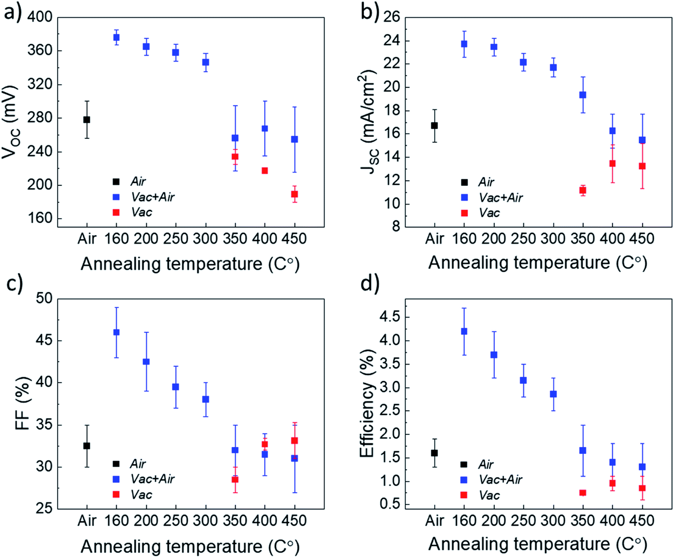 | ||
| Fig. 3 J–V parameters, including (a) open-circuit voltage – VOC, (b) short-circuit current density – JSC, (c) fill factor – FF and (d) efficiency of TiO2/Sb2Se3 devices with different TiO2 annealing conditions. | ||
It is clear from Fig. 3 that the devices annealed according to the Vac+Air approach gained a significant boost in performance over devices that were subject to just one of the two other annealing procedures. All J–V parameters showed higher values for a combined Vac+Air procedure in the temperature range of 160–300 °C, with the Vac+Air procedure carried out at 160 °C enabling the best device performance of 4.7%. The J–V characteristics and EQE spectral response of the representative 4.7% efficient device are shown in Fig. 4a and b. The increase of the annealing temperature beyond 160 °C in the Vac+Air procedure caused all solar cell parameters to slightly worsen. Also important to note is the fact that the Vac+Air annealing of TiO2 layers at temperatures in the range of 350 to 450 °C causes devices to produce lower JSC values than devices with Vac annealed TiO2 layers (Fig. 3). Considering the differences in the solar cell efficiencies (Fig. 3), one could emphasize that the grain structure and texture of the Sb2Se3 absorber films deposited on either Vac, Vac+Air, or Air annealed TiO2 should be reflected in the final device performance. Looking at the top- and cross-sectional view SEM images of Sb2Se3 absorber films deposited onto Vac160°C+Air (Fig. 5a and b) and Vac450°C+Air (Fig. 5c and d) annealed TiO2, no detectable changes in the grain morphology of the absorber were observed. Independent of the TiO2 annealing procedure, the absorber growth follows a similar morphology of columnar sintered grains (Fig. 5b and d).
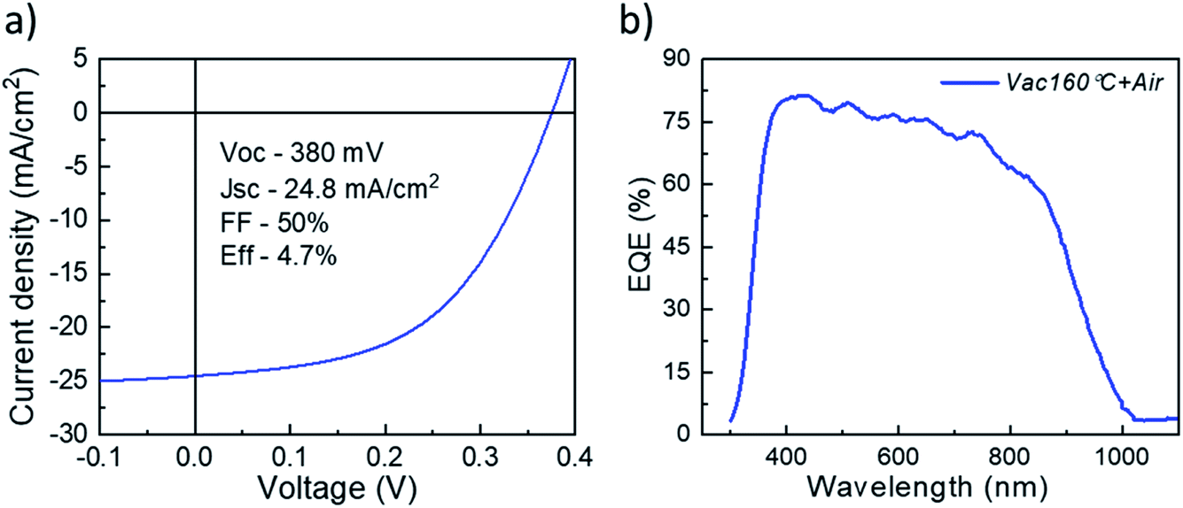 | ||
| Fig. 4 (a) J–V characteristics and (b) EQE spectral response of the representative 4.7% efficiency device. | ||
 | ||
| Fig. 5 Top-and cross-sectional view SEM images of CSS Sb2Se3 absorber films deposited at 460 °C onto TiO2/FTO/glass stacked substrates, with (a and b) 160 °C vacuum and consequent 450 °C air annealed TiO2 and (c and d) 450 °C vacuum and consequent 450 °C air annealed TiO2 layers. | ||
Analysis of the XRD patterns of the Sb2Se3 absorber deposited onto Vac+Air and Vac annealed TiO2 layers (Fig. 6a and b) and the related texture coefficients (Fig. 6c and d) reveals that independent of the TiO2 annealing, the absorber exhibits preferential orientation along the (211), (221) and (002) planes.
 | ||
| Fig. 6 XRD patterns of CSS Sb2Se3 absorber films deposited at 460 °C onto TiO2/FTO/glass stacked substrates, with (a) vacuum and subsequent air annealed (Vac+Air) TiO2 and (b) vacuum annealed only (Vac) TiO2 layers. Related texture coefficients (TC) for (c) vacuum and subsequent air annealed (Vac+Air) and (d) vacuum annealed (Vac) films, calculated from the integrated intensity ratios (using the Harris formula46) for the dominant miller planes of Sb2Se3. | ||
These peaks are characteristic of the orthorhombic Sb2Se3 crystal structure (PDF card no. 01-089-0821) and match well with those reported in the literature for the Sb2Se3 absorber deposited by the CSS and VTD techniques.32–35 Although there could be other changes at the nanoscale of the absorber (grain interior to grain boundaries), these results indicate that the quality of the main Sb2Se3–TiO2 interface (which is determined by the annealing approach of TiO2) is the main parameter which affects the solar cell performance in Fig. 3. The optimum efficiency point found for 160 °C TiO2 vacuum annealing may be explained through the combined effect of reduced carbon content in the vacuum annealing step and oxygen-included recrystallization of the film during the following 450 °C air annealing step. A low carbon content at the Sb2Se3–TiO2 main interface implies an improved heterojunction formation (and, probably, a lower concentration of the interface defect states), resulting in an increased performance of the solar cell (Fig. 3).
So far, our results indicate that the vacuum annealing of TiO2 can be a suitable processing step for decreasing the concentration of organic residual species in TiO2 and, by this, to improve the heterojunction quality and cell efficiency. However, the treatment needs to be performed at a moderate temperature (≤200 °C) so as to keep the TiO2 grain sizes small enough for their active recrystallization in the subsequent air annealing step at 450 °C. On the other hand, the low solar cell efficiency obtained with only Vac annealed TiO2 (i.e., without subsequent 450 °C air treatment) indicates the necessity of oxygen-rich conditions during the recrystallization of USP deposited TiO2.
To provide support for the above statements, especially on the concentration of carbon species at the TiO2 surface, we further analyzed the annealed TiO2 films by XPS. The XPS spectra were registered from the surface of ∼80 nm thick USP TiO2 films deposited at 340 °C onto FTO/glass substrates. Since no distinguishable differences were observed between the spectra of the as deposited and annealed TiO2, only one survey spectrum of the as-deposited TiO2 film is illustrated in Fig. 7a. The binding energy (BE) values, as well as the shape of the Ti 2p3/2 and O 1s core level peaks (not shown here), are characteristics of single-phase anatase TiO2 films.28 Emission of the Sn 3d5/2 core level from the underlying FTO substrate is registered only in the case of the as-deposited film and can be related to the presence of some pinholes in the TiO2 film. No secondary phases were revealed in any of the as deposited or annealed TiO2 films, supporting the above-mentioned XRD results (Fig. 1).
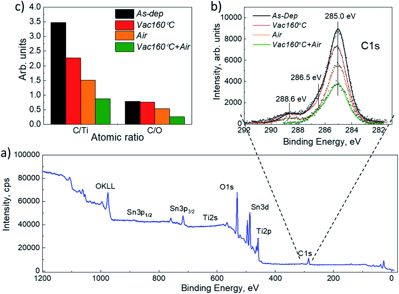 | ||
| Fig. 7 (a) XPS survey spectrum of TiO2 films deposited by USP at 340 °C onto FTO/glass substrates. (b) C 1s core level from the as deposited (labelled as As-dep), 160 °C vacuum annealed (labelled as Vac160°C), 450 °C air annealed (labelled as Air), 160 °C vacuum and subsequent 450 °C air annealed (Vac160°C+Air) TiO2 films. (c) Calculated atomic ratios C/Ti and C/O for the related samples. | ||
To clarify the evolution of carbon impurities at the surface of the annealed TiO2 films, we analyzed the C 1s core level emission. We cannot quantify the air contamination of the measured surfaces but, keeping in mind that all the TiO2 samples spent the same time in air from the UPS until the XPS analysis, we assume that a similar amount of carbon species from the air contamination is present on all analyzed samples and the differences in the C 1s signal can be attributed to the fluctuation of other carbon species from the near surface bulk of the TiO2 film. The C 1s peak contains three features at BE values of 285.0 eV, 286.5 eV, and 288.6 eV (Fig. 7b). The highest peak located at 285.0 eV originates from the C![[double bond, length as m-dash]](https://www.rsc.org/images/entities/char_e001.gif) C bond. Peaks with the BE values 286.5 eV and 288.6 eV represent the oxygen-bound species C–O and Ti–O–C bonds, respectively.36 These peaks, and especially the one at 288.6 eV, confirm the incorporation of carbon into the TiO2 lattice.37 Therefore, we consider the C 1s emission at 288.6 eV as evidence of so-called organic residuals of the USP precursor solution (TTIP complex, together with oxygen, and carbon from AcacH) and analyze how they are affected by the annealing of TiO2.
C bond. Peaks with the BE values 286.5 eV and 288.6 eV represent the oxygen-bound species C–O and Ti–O–C bonds, respectively.36 These peaks, and especially the one at 288.6 eV, confirm the incorporation of carbon into the TiO2 lattice.37 Therefore, we consider the C 1s emission at 288.6 eV as evidence of so-called organic residuals of the USP precursor solution (TTIP complex, together with oxygen, and carbon from AcacH) and analyze how they are affected by the annealing of TiO2.
Fig. 7b and Table 1 show that the as-deposited TiO2 films contain the most intense C 1s emission at 288.6 eV and vacuum (Vac) annealing at 160 °C slightly decreased it. Such a low annealing temperature seems to be insufficient for a significant reduction of carbon. An air treatment at 450 °C further reduced the concentration of the carbon, however, the lowest intensity of 288.6 eV emission was observed for the combination of the two steps, Vac160°C and subsequent Air 450 °C annealing of TiO2 (Fig. 7). Interestingly, in the case of the Vac+Air treated samples, the concentration of oxygen was found to be much higher compared with those from the Vac annealed samples (63.5 at% vs. 52.5 at%, Table 1).
| Sample | C 1s, at% | N 1s, at% | O 1s, at% | Ti 2p3/2, at% |
|---|---|---|---|---|
| As-dep | 38.3 | 1.8 | 48.3 | 11.8 |
| Vac | 36 | 0.6 | 47.6 | 15.9 |
| Air | 28.2 | 0.6 | 52.5 | 18.7 |
| Vac+Air | 16.3 | 1.5 | 63.5 | 18.8 |
The XPS results prove that the organic residuals of the USP precursor solution are not easily removed as vapors of H2O and CO and CO2 gas at the stage of the USP deposition at 340 °C and during post-deposition air treatment at 450 °C. A few recent studies from the photocatalysis field have shown the presence of carbon species in USP TiO2 films after air annealing at temperatures ≥500 °C and after additional ultraviolet treatments.38
Moreover, the carbon was found to be beneficial for the photocatalytic performance of TiO2.39 The same TTIP–AcacH based precursor solution is widely used for the spin coating and USP deposition of planar TiO2 films as an electron transport layer in perovskite solar cells.40,41 In particular, for TiO2 based perovskites, a single step air treatment at 450–500 °C is a well-established annealing step and there is little to no impact of the AcacH concentration (over a wide range from 1:10 to 1:20 TTIP:AcacH ratios) on the perovskite device performance.42,43 Our results instead bring experimental evidence that the USP precursor and annealing procedures for TiO2 strongly impact the efficiency of Sb2Se3/TiO2 solar cells. Based on XPS data (and changes in the lattice parameters of TiO2), we show that the residual carbon species (Fig. 7b) play an important role in the composition of the surface and bulk defects in TiO2. This effect is then translated into the quality of the Sb2Se3–TiO2 heterointerface formation and subsequently has a great impact on the final device performance. We demonstrate that vacuum annealing could be a suitable technological approach to decrease the concentration of carbon species in TiO2 films and, by this, to improve the performance of Sb2Se3 solar cell efficiency. However, more research efforts are required to understand the correlation between the USP precursor solution, residual organic species, and TiO2 surface defects and, thus, their impact on the TiO2–Sb2Se3 interface, related interface defect states, and final device performance. In this direction, a combination of advanced characterization methods, such as scanning transmission electron microscopy (STEM)44 and transient SPV spectroscopy,45 could be suitable techniques to gain in-depth insights into the impact of nanoscale carbon species on GBs electronic properties in TiO2 and passivation of the electronic traps at the main interface.
Conclusions
In this work, we systematically study the impact of TiO2 annealing conditions on the performance of Sb2Se3/TiO2 thin film solar cells. The results were compared for three annealing variations: vacuum annealing only at 160–450 °C, two-step vacuum annealing at 160–450 °C followed by a subsequent 450 °C air treatment, and 450 °C air treatment only. XRD and SEM analysis showed improved structural properties of the TiO2 when a two-step annealing was applied. We showed that vacuum annealing can be a suitable technological approach to decrease the concentration of organic residues in TiO2 films. Changes in the lattice parameters of annealed TiO2 indicated the processes taking place inside the crystalline lattice of the TiO2 films and were connected with the removal of residual species. The annealing conditions do not affect the grain structure of the Sb2Se3 absorber films but significantly impact the final device performance. The employment of one step TiO2 vacuum annealing has a detrimental impact on the cell efficiency. Vacuum annealing at 160 °C followed by subsequent 450 °C air treatment led to a 4.7% device performance. This was explained by achieving an optimal balance between the removal of carbon content during vacuum annealing and the active recrystallization of TiO2 during air annealing. The decrease of the carbon concentration by employing the two-step approach was proven by XPS. Our findings pave a solid platform for further research investigations on the impact of organic residues in chemically processed TiO2, including optimization of post deposition treatments for efficient Sb2Se3 solar cells.Author contributions
Mykhailo Koltsov: conceptualization, data curation, formal analysis, methodology, software, visualization, writing – original draft. Robert Krautmann: software, visualization, writing – review & editing. Atanas Katerski: formal analysis, writing – review & editing. Natalia Maticiuc: formal analysis, writing – review & editing, validation. Malle Krunks: formal analysis, validation. Ilona Oja Acik: validation, project administration, funding acquisition. Nicolae Spalatu: conceptualization, formal analysis, methodology, supervision, visualization, writing – review & editing, validation and funding acquisition.Conflicts of interest
There are no conflicts to declare.Acknowledgements
This study was funded by the Estonian Research Council project PRG627 “Antimony chalcogenide thin films for next-generation semi-transparent solar cells applicable in electricity producing windows”, the Estonian Research Council project PSG689 “Bismuth Chalcogenide Thin-Film Disruptive Green Solar Technology for Next Generation Photovoltaics”, the Estonian Centre of Excellence project TK141 (TAR16016EK) “Advanced materials and high-technology devices for energy recuperation system”, and the EU H2020 program under the ERA Chair project 5GSOLAR grant agreement no. 952509.Notes and references
- N. Spalatu, J. Hiie, R. Kaupmees, O. Volobujeva, J. Krustok, I. O. Acik and M. Krunks, ACS Appl. Mater. Interfaces, 2019, 11, 17539–17554 CrossRef CAS PubMed.
- N. C. Miller and M. Bernechea, APL Mater., 2018, 6, 084503 CrossRef CAS.
- D. Tiwari, O. S. Hutter and G. Longo, J. Phys.: Energy, 2021, 3, 034010 CAS.
- A. Zakutayev, Rapid Development of Disruptive Photovoltaic Technologies, 2019 Search PubMed.
- T. D. C. Hobson, L. J. Phillips, O. S. Hutter, H. Shiel, J. E. N. Swallow, C. N. Savory, P. K. Nayak, S. Mariotti, B. Das, L. Bowen, L. A. H. Jones, T. J. Featherstone, M. J. Smiles, M. A. Farnworth, G. Zoppi, P. K. Thakur, T.-L. Lee, H. J. Snaith, C. Leighton, D. O. Scanlon, V. R. Dhanak, K. Durose, T. D. Veal and J. D. Major, Chem. Mater., 2020, 32, 2621–2630 CrossRef CAS.
- R. Krautmann, N. Spalatu, R. Gunder, D. Abou-Ras, T. Unold, S. Schorr, M. Krunks and I. Oja Acik, Sol. Energy, 2021, 225, 494–500 CrossRef CAS.
- I. Caño, P. Vidal-Fuentes, L. Calvo-Barrio, X. Alcobé, J. M. Asensi, S. Giraldo, Y. Sánchez, Z. Jehl, M. Placidi, J. Puigdollers, V. Izquierdo-Roca and E. Saucedo, ACS Appl. Mater. Interfaces, 2022, 14, 11222–11234 CrossRef PubMed.
- C. Chen, W. Li, Y. Zhou, C. Chen, M. Luo, X. Liu, K. Zeng, B. Yang, C. Zhang, J. Han and J. Tang, Appl. Phys. Lett., 2015, 107, 043905 CrossRef.
- Z. Li, X. Liang, G. Li, H. Liu, H. Zhang, J. Guo, J. Chen, K. Shen, X. San, W. Yu, R. E. I. Schropp and Y. Mai, Nat. Commun., 2019, 10, 1 CrossRef PubMed.
- J. S. Eensalu, A. Katerski, E. Kärber, L. Weinhardt, M. Blum, C. Heske, W. Yang, I. Oja Acik and M. Krunks, Beilstein J. Nanotechnol., 2019, 10, 2396–2409 CrossRef CAS PubMed.
- Y. Zhao, S. Wang, C. Jiang, C. Li, P. Xiao, R. Tang, J. Gong, G. Chen, T. Chen, J. Li and X. Xiao, Adv. Energy Mater., 2022, 12, 2103015 CrossRef CAS.
- N. Spalatu, R. Krautmann, A. Katerski, E. Karber, R. Josepson, J. Hiie, I. O. Acik and M. Krunks, Sol. Energy Mater. Sol. Cells, 2021, 225, 111045 CrossRef CAS.
- L. J. Phillips, C. N. Savory, O. S. Hutter, P. J. Yates, H. Shiel, S. Mariotti, L. Bowen, M. Birkett, K. Durose, D. O. Scanlon and J. D. Major, IEEE J. Photovolt., 2019, 9, 544–551 Search PubMed.
- X. Wen, C. Chen, S. Lu, K. Li, R. Kondrotas, Y. Zhao, W. Chen, L. Gao, C. Wang, J. Zhang, G. Niu and J. Tang, Nat. Commun., 2018, 9, 1 CrossRef PubMed.
- H. Shiel, O. S. Hutter, J. E. N. Swallow, L. A. Jones, T. J. Featherstone, M. J. Smiles, P. K. Thakur, L. J. Phillips, K. Durose, J. D. Major, V. R. Dhanak, T.-L. Lee and T. D. Veal, Band Alignment Measurements of Sb2Se3 Solar Cells Using HAXPES, 2015 Search PubMed.
- L. Wang, D. B. Li, K. Li, C. Chen, H. X. Deng, L. Gao, Y. Zhao, F. Jiang, L. Li, F. Huang, Y. He, H. Song, G. Niu and J. Tang, Nat. Energy, 2017, 2, 17046 CrossRef CAS.
- V. Kumar, E. Artegiani, P. Punathil, M. Bertoncello, M. Meneghini, F. Piccinelli and A. Romeo, ACS Appl. Energy Mater., 2021, 4, 12479–12486 CrossRef CAS.
- A. Stoliaroff, A. Lecomte, O. Rubel, S. Jobic, X. H. Zhang, C. Latouche and X. Rocquefelte, ACS Appl. Energy Mater., 2020, 3, 2496–2509 CrossRef CAS.
- T. Potlog, N. Spalatu, N. Maticiuc, J. Hiie, V. Valdna, V. Mikli and A. Mere, Phys. Status Solidi A, 2012, 209, 272–276 CrossRef CAS.
- J. Ramanujam, D. M. Bishop, T. K. Todorov, O. Gunawan, J. Rath, R. Nekovei, E. Artegiani and A. Romeo, Prog. Mater. Sci., 2020, 110, 100619 CrossRef CAS.
- J. Andrade-Arvizu, R. F. Rubio, V. Izquierdo-Roca, I. Becerril-Romero, D. Sylla, P. Vidal-Fuentes, Z. J. Li-Kao, A. Thomere, S. Giraldo, K. Tiwari, S. Resalati, M. Guc and M. Placidi, ACS Appl. Mater. Interfaces, 2022, 14, 1177–1186 CrossRef CAS PubMed.
- N. Maticiuc, N. Spalatu, V. Mikli and J. Hiie, in Applied Surface Science, Elsevier B.V., 2015, vol. 350, pp. 14–18 Search PubMed.
- Y. Zhou, Y. Li, J. Luo, D. Li, X. Liu, C. Chen, H. Song, J. Ma, D. J. Xue, B. Yang and J. Tang, Appl. Phys. Lett., 2017, 111, 013901 CrossRef.
- U. Diebold, Surf. Sci. Rep., 2003, 48, 53–229 CrossRef CAS.
- J. S. Eensalu, A. Katerski, E. Kärber, I. O. Acik, A. Mere, M. Krunks, J. S. Eensalu, A. Katerski, E. Kärber, I. O. Acik, A. Mere and M. Krunks, Beilstein J. Nanotechnol., 2019, 10, 198–210 CrossRef PubMed.
- N. Spalatu, R. Krautmann, A. Katerski, E. Karber, R. Josepson, J. Hiie, I. O. Acik and M. Krunks, Sol. Energy Mater. Sol. Cells, 2021, 225, 111045 CrossRef CAS.
- N. Maticiuc, T. Kodalle, J. Lauche, R. Wenisch, T. Bertram, C. A. Kaufmann and I. Lauermann, Thin Solid Films, 2018, 665, 143–147 CrossRef CAS.
- I. Dundar, M. Krichevskaya, A. Katerski and I. O. Acik, R. Soc. Open Sci., 2019, 6, 181578 CrossRef CAS PubMed.
- J.-C. Lee, A.-I. Gopalan, G. Saianand, K.-P. Lee and W.-J. Kim, Nanomaterials, 2020, 10, 456 CrossRef CAS PubMed.
- M. Reticcioli, I. Sokolović, M. Schmid, U. Diebold, M. Setvin and C. Franchini, Phys. Rev. Lett., 2019, 122, 016805 CrossRef CAS PubMed.
- U. Diebold, Surf. Sci. Rep., 2003, 48, 53–229 CrossRef CAS.
- Z. Li, X. Liang, G. Li, H. Liu, H. Zhang, J. Guo, J. Chen, K. Shen, X. San, W. Yu, R. E. I. Schropp and Y. Mai, Nat. Commun., 2019, 10, 1 CrossRef PubMed.
- X. Wen, C. Chen, S. Lu, K. Li, R. Kondrotas, Y. Zhao, W. Chen, L. Gao, C. Wang, J. Zhang, G. Niu and J. Tang, Nat. Commun., 2018, 9, 1 CrossRef PubMed.
- A. Chirilǎ, P. Reinhard, F. Pianezzi, P. Bloesch, A. R. Uhl, C. Fella, L. Kranz, D. Keller, C. Gretener, H. Hagendorfer, D. Jaeger, R. Erni, S. Nishiwaki, S. Buecheler and A. N. Tiwari, Nat. Mater., 2013, 12, 1107–1111 CrossRef PubMed.
- J. Yang, Y. Lai, Y. Fan, Y. Jiang, D. Tang, L. Jiang, F. Liu and J. Li, RSC Adv., 2015, 5, 85592–85597 RSC.
- Y. Zhang, Z. Zhao, J. Chen, L. Cheng, J. Chang, W. Sheng, C. Hu and S. Cao, Appl. Catal., B, 2015, 165, 715–722 CrossRef CAS.
- R. Klaysri, M. Ratova, P. Praserthdam and P. Kelly, Nanomaterials, 2017, 7, 113 CrossRef PubMed.
- I. Dundar, M. Krichevskaya, A. Katerski, M. Krunks and I. O. Acik, Catalysts, 2019, 9, 915 CrossRef CAS.
- J. Spiridonova, A. Mere, M. Krunks, M. Rosenberg, A. Kahru, M. Danilson, M. Krichevskaya and I. Oja Acik, Catalysts, 2020, 10, 1011 CrossRef CAS.
- J. Sun, A. R. Pascoe, S. Meyer, Q. Wu, E. della Gaspera, S. R. Raga, T. Zhang, A. Nattestad, U. Bach, Y.-B. Cheng and J. J. Jasieniak, Sol. Energy, 2019, 188, 697–705 CrossRef CAS.
- A. Möllmann, D. Gedamu, P. Vivo, R. Frohnhoven, D. Stadler, T. Fischer, I. Ka, M. Steinhorst, R. Nechache, F. Rosei, S. G. Cloutier, T. Kirchartz and S. Mathur, Appl. Catal., B, 2019, 21, 1801196 Search PubMed.
- K. Wojciechowski, M. Saliba, T. Leijtens, A. Abate and H. J. Snaith, Energy Environ. Sci., 2014, 7, 1142–1147 RSC.
- L. Kegelmann, C. M. Wolff, C. Awino, F. Lang, E. L. Unger, L. Korte, T. Dittrich, D. Neher, B. Rech and S. Albrecht, ACS Appl. Mater. Interfaces, 2017, 9, 17245–17255 CrossRef CAS PubMed.
- J. A. Quirk, B. Miao, B. Feng, G. Kim, H. Ohta, Y. Ikuhara and K. P. McKenna, Nano Lett., 2021, 21, 9217–9223 CrossRef CAS PubMed.
- Th. Dittrich, L. E. Valle Rios, S. Kapil, G. Gurieva, N. Rujisamphan and S. Schorr, Appl. Phys. Lett., 2017, 110, 023901 CrossRef.
- H. J. Bunge, Textures Microstruct., 1997, 29, 1–26 CrossRef CAS.
| This journal is © The Royal Society of Chemistry 2022 |