
Photoelectrocatalytic production of solar fuels with semiconductor oxides: materials, activity and modeling
Damián
Monllor-Satoca
 ,
María Isabel
Díez-García†
,
Teresa
Lana-Villarreal
and
Roberto
Gómez
*
,
María Isabel
Díez-García†
,
Teresa
Lana-Villarreal
and
Roberto
Gómez
*
Departament de Química Física i Institut Universitari d'Electroquímica, Universitat d'Alacant, Apartat 99, E-03080, Alicante, Spain. E-mail: roberto.gomez@ua.es
First published on 9th September 2020
Abstract
Oxide photoelectrochemistry has been under continuous development over the last half century. These decades have witnessed the use of electrodes of different nature (from single crystals to nanoparticulate films), new electrode materials (including ternary and multinary transition metal oxides), and different strategies for improving their efficiency and stability (e.g. doping or protective layers). Although the very high initial expectations for using oxide electrodes in solar energy conversion were not fully met, substantial efforts have been devoted to reach an in-depth understanding of the processes limiting their functioning, providing firm bases for further developments. In this article, we review our main contributions in this field; in particular, we focus on the water photooxidation (i.e. oxygen evolution reaction), water photoreduction (i.e. hydrogen evolution reaction) and full water splitting processes (in a tandem cell) with binary and ternary oxides, including metal hydroxides as co-catalysts. We emphasize the importance of modeling and obtaining mechanistic insights and we conclude with a reflection on the main issues to be tackled in this field, which in our opinion should experience major advances in the coming years.
 Damián Monllor-Satoca | D. Monllor-Satoca (BSc and MSc in Chemistry) received a PhD in Materials Science, supervised by Prof. R. Gómez (University of Alicante, 2010). He did a Postdoctoral stay in the Pohang University of Science and Technology (POSTECH, South Korea), with Prof. W. Choi. Then, he moved back to Spain to the Catalonia Institute of Energy Research (IREC) as a Researcher with Prof. J. R. Morante, and later to the IQS-University Ramon Llull as a Lecturer. He presently works as Senior Researcher in the University of Alicante. His research interests include: (1) semiconductor photoelectrochemistry, (2) artificial photosynthesis, and (3) heterogeneous photo(electro)catalysis for environmental applications. |
 María Isabel Díez-García | M. I. Díez-García studied Chemical Engineering at the University of Alicante, where she also obtained a Master in Materials Science. In 2018, she received her PhD for the study of metal oxide photocathodes for solar energy conversion in the research group of “Photochemistry and Electrochemistry of Semiconductors” under the supervision of Prof. R. Gómez at the University of Alicante. She later continued for two years as a postdoctoral researcher with the same group. Most recently, she joined the Catalonia Institute for Energy Research (IREC) as a Juan de la Cierva postdoctoral fellow with Prof. J. R. Morante. Among her research interests are the fundamentals and applications of (photo)electrochemistry for energy conversion. |
 Teresa Lana-Villarreal | T. Lana-Villarreal obtained her diploma in Chemistry in 1999 from the University of Navarra (Spain). During her PhD, she mainly worked on the photooxidation mechanism of organics on TiO2 electrodes at the University of Poitiers (France) and at the University of Alicante (Spain). She made a postdoctoral stay with Prof. A. Hagfeldt at KTH (Sweden) on DSSC. Afterwards, she moved back to the University of Alicante where she joined the research group of “Photochemistry and Electrochemistry of Semiconductors” lead by Prof. R. Gómez and became associate professor in 2011. Her research activities include fundamental aspects of metal oxide semiconductors and their use in technological applications. |
 Roberto Gómez | R. Gómez obtained his PhD from the University of Alicante (Spain) in 1994 working on the Pt-group single crystal electrochemistry. After a postdoctoral stay at Purdue University (USA), he moved back to Alicante where he currently is professor of physical chemistry and leads the group of Semiconductor Photochemistry and Electrochemistry. In 1999 he was a visiting scientist at Bath University (UK) with Prof. Peter and a year later at the National Renewable Energy Laboratory (USA) with Dr Nozik. His research interests include semiconductor electrochemistry (applied to solar fuel generation), alkaline and alkaline-earth batteries, green electrochemistry and sonochemistry. |
Introduction
Utilization of solar energy
Solar light represents a clean, abundant, cheap and (virtually) endless energy source1,2 that could be used for transitioning the energy needs of our society to a more environmentally friendly, less polluting and less fossil-fuel dependent economy. However, its intermittency represents a major bottleneck to its widespread use, requiring convenient materials and technologies that could efficiently absorb, use and store it.3,4 At the core of this technology is the use of semiconductor materials (photocatalysts, either as powder suspensions or thin films), characterized by an energy band gap that allows them to absorb light and generate electrons and holes that could drive charge transfer processes when interfaced with a solution with appropriate redox couples.3,5,6 Two main environmental and energy applications find their way through heterogeneous photocatalysis:7,8 (i) the degradation of noxious substances (photocatalysis), and (ii) the generation of value-added chemicals (photosynthesis). However, as Osterloh6 and Rajeshwar4 recently stated, these applications are often confused in the literature, and even the IUPAC sometimes uses misleading definitions.9To understand their differences, we should invoke: (i) their thermodynamics, (ii) the charge transfer processes,10 and (iii) the overall energy balance. Regarding the first, a reaction energy diagram is required (Fig. 1, top); in photocatalysis, the reaction proceeds “down-hill” and the change on the reaction Gibbs energy (ΔG) is negative, thus the process is spontaneous; however, in photosynthesis the reaction proceeds “up-hill”, the reaction ΔG is positive and the process non-spontaneous.3 As for the second issue, recalling the semiconductor band diagrams11,12 (Fig. 1, down), the electrons and holes are respectively transferred to electron acceptors (A) or donors (D), but their relative positions with respect to the band edges determine whether the process is photocatalytic or photosynthetic. Finally, in terms of the energy balance,5,6 the photocatalytic process uses light to accelerate the reaction rate, whereas the photosynthetic process effectively stores light energy as chemicals. In this regard, the process of artificial photosynthesis5 to store solar energy as on-demand fuels (e.g. hydrogen, methanol, etc.) is considered one of the “holy grails” in chemistry and a way to circumvent the solar intermittency.
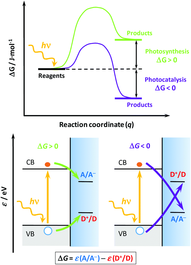 | ||
| Fig. 1 Schemes for the energy vs. reaction coordinate curve (top) and the corresponding band structures (down) for two generic processes: photosynthetic (down left, green lines) and photocatalytic (down right, purple lines). Symbols: CB and VB, conduction and valence bands, respectively; A/A−, redox couple associated with the electron acceptor (A); D+/D, redox couple associated with the electron donor or hole acceptor (D); ΔG, Gibbs energy of reaction; ε, energy in the absolute scale; hν, photon energy; q, reaction coordinate. The equation below shows how to calculate ΔG from the energies of each redox couple. Grey and blue shaded areas represent the filled VB states and the electrolyte, respectively. The top scheme was adapted from ref. 6, and the down scheme was adapted from ref. 11 and 12. | ||
Photoelectrocatalysis
In spite of the promising environmental applications and good prospects of heterogeneous photocatalysis, the process generally suffers from a series of demerits, including: (i) a high rate of electron–hole recombination that can be faster than their interfacial transfer rates,10 and (ii) a sluggish kinetics for the redox processes occurring on the surface of the bare photocatalyst.13 One strategy to partially ameliorate these limitations is the application of an external potential bias with the semiconductor as a film supported on a conducting substrate (photoelectrode), thus electrochemically assisting the photocatalytic process.9 This bias is applied with respect to the counter electrode, which selectively drives one of the charge carriers out of the illuminated semiconductor film, concomitantly increasing the charge transfer rate of the carriers remaining at the surface of the semiconductor and decreasing the recombination rate.14In comparison with conventional photocatalysis (PC), photoelectrocatalysis (PEC): (i) is performed with semiconductor films on conducting substrates, while PC can be performed with both suspensions or films on non-conducting substrates, (ii) operates under an applied external potential, while PC operates under open-circuit conditions (no external bias), (iii) anodic and cathodic processes can be individually studied or enhanced with the appropriate bias, while in PC, both processes occur simultaneously at the photocatalyst surface, (iv) the electron and hole fluxes are not the same and thus a net photocurrent is recorded, while in PC the flux of both carriers is the same, and (v) the energy efficiency is lower than in PC, as the PEC bias represents an extra energy supply to drive the desired reactions.
Layout of the manuscript
In this feature article, we will revise the main contributions of the authors to the field of photoelectrocatalysis with semiconductor electrodes, in particular to produce solar fuels. We will first discuss the features of metal (hydr-)oxides as electrodes, including experimental and theoretical strategies to improve their performance. Next, we will revise the electrochemical behavior of metal oxides, both as compact or nanostructured thin films, and how electrochemical measurements can be used to elucidate their electronic structure, as well as the nature of surface and/or trap states. Then, we will review the use of binary and ternary oxides for water photooxidation (oxygen evolution reaction, OER), water photoreduction (hydrogen evolution reaction, HER) and combined in a tandem cell (full water splitting), including the use of metal hydroxides as co-catalysts; particular emphasis will be given to modeling the charge transfer processes of these systems and the mechanistic information that could be gained from them. To conclude, a reflective outlook that both accounts for the main issues that remain to be addressed and tries to shed some light on the future of this research field will also be given.The performance of metal oxides under illumination
Metal oxides and hydroxides as electrodes
The features of the (photo)electrodes are vital to ensure that they efficiently harvest and utilize solar energy,15 while showing potential for their upscaling and implementation in practical devices.16 As such, the semiconductors to be employed must meet some stringent requirements, including:15,17–19 (i) absorb most of the useful solar spectrum, mainly composed of visible light (optical constraints); (ii) efficiently separate and transport charge carriers through the material to the appropriate interfaces (spatial charge constraints); (iii) efficiently transfer charge carriers at the semiconductor–electrolyte interface (SEI) to the appropriate redox couples (charge transfer constraints); and (iv) be inexpensive, abundant, non-toxic and durable upon many operation cycles (availability and stability constraints).Among the most used materials in photoelectrocatalysis are metal oxides and hydroxides,19,20 both as photocatalysts and electrocatalysts (i.e. co-catalysts).13,21,22 Some of the advantages of these materials are: (i) chemical stability in different aqueous media and under illumination, (ii) appropriate position of band edges15,18,19,23,24 for driving many redox processes, (iii) low cost, and (iv) straightforward synthesis and processing. However, they are generally limited by:18,19 (i) slow charge transfer kinetics at the surface (i.e. large overpotentials for different redox processes), (ii) relatively wide band gaps that prevent the absorption of a large portion of the solar spectrum, and (iii) large surface density of defects that portray increased charge recombination.20 Binary oxides have been by far the most studied as both photoanodes and photocathodes;25 however, ternary oxides (e.g. spinels, delafossites, perovskites and scheelites) have also emerged as promising materials due to their potentially narrow band gaps, which allow them to absorb a large portion of the visible solar spectrum.26 A detailed description of the features of different oxides and hydroxides used in (photo)electrocatalysis can be found elsewhere.19,20,23
Strategies to improve the photoelectrocatalytic activity
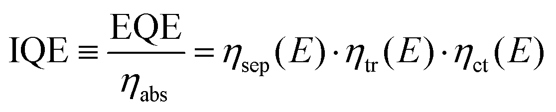
Prior to discussing how to improve the performance of semiconductor electrodes, we should first analyze the factors influencing their efficiency. As a reference magnitude, we shall take the potential-dependent photocurrent density (jph(E), A cm−2) from which the overall external or internal quantum efficiencies can be easily obtained (EQE or IQE, eqn (1) and (2) respectively):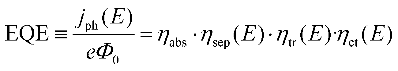 | (1) |
 | (2) |
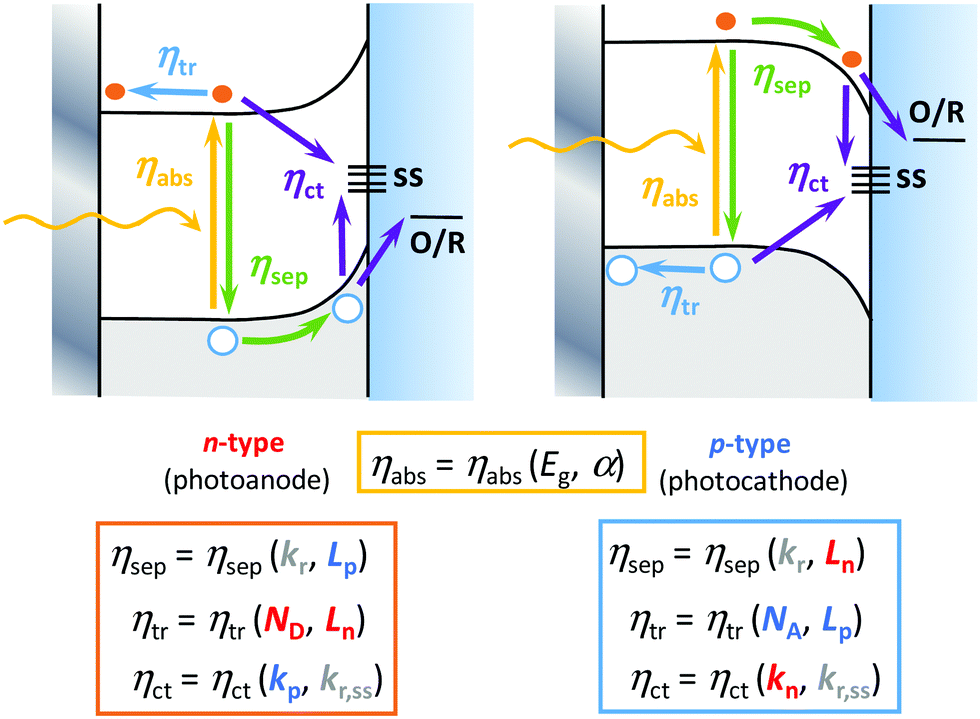 | ||
| Fig. 2 Scheme with the band structure and the semiconductor electrolyte interface (SEI) depicting the efficiencies (η) for all the light-induced processes as a function of different physical magnitudes, in the case of an n-type photoanode (left) and a p-type photocathode (right). Symbols: ηabs (yellow), ηsep (green), ηtr (blue) and ηct (purple) refer to the efficiencies of light absorption, charge separation, majority charge carrier transport, and minority charge carrier transfer processes, respectively; Eg, band gap energy; α, light absorption coefficient; ss, surface states; O/R, dissolved or adsorbed redox couple at the SEI; kn and kp, minority carrier transfer rate constants for electrons and holes at the SEI, respectively; kr and kr,ss, charge recombination rate constants in the bulk and at surface states, respectively; Ln and Lp, diffusion lengths of electrons (majority carriers in photoanodes, minority carriers in photocathodes) and holes (majority carriers in photocathodes, minority carriers in photoanodes), respectively; ND and NA, charge donor or acceptor densities in n- or p-type semiconductors, respectively. | ||
Interestingly, it is possible to improve most of the individual efficiencies by tuning some semiconductor properties, including (Fig. 2): (i) optical properties that affect ηabs, including the band gap width and the absorption coefficient; (ii) electronic structure, which affects ηsep(E) and ηtr(E), including the band edge positions and carrier mobility; (iii) crystallinity, which affects ηtr(E), including the rates of bulk recombination and diffusion-drift; and (iv) surface properties that affect ηct(E), including the rates of carrier transfer and surface recombination.31 Among the experimental strategies employed to improve these efficiencies, we could briefly mention:32 (i) bulk doping to change the conductivity of the material (ηtr(E)) and the width of the band gap (ηabs), (ii) nano- or mesostructuring to change the charge carriers’ diffusion rates (ηsep(E) and ηtr(E)) and surface transfer rates (ηct(E)),23,24 (iii) compositing with other metals or semiconductors to generate homo- or heterojunctions to change the charge separation, transport or optical properties, (iv) surface modification31 to change the catalytic properties (ηct(E)) and light absorption, by means of: optical sensitization, passivation or protective thin layers, co-catalysts and interfacial conditioning (through the adsorption of inert ions or dipoles).32 As these strategies are beyond the scope of this article, we refer here the readers to excellent recent reviews that cover them in more depth.10,13,17,27,33
Importance of modeling
To better guide the choice of materials and the modification strategy that could enhance the performance of the metal (hydr-)oxide (photo)electrode, it is paramount to model the (photo)electrochemical behavior of the system.34,35 This modeling can be performed at three levels: that of the materials, that of the electrode charge dynamics, and that of the full devices.The material-level modeling is based on computational approaches to obtain the electronic structure,36 being dominant the DFT calculations. They are used in this context to identify metal and non-metal combinations (binary or multinary) yielding optimum electronic structure (band engineering) to thermodynamically and kinetically drive the desired redox processes and absorb most of the solar spectrum. It is worth noting that, together with the computational approach, a combinatorial approach can also be followed to individuate candidates for photoelectrodes,37 with a benchmarking experimental procedure that can readily map out the best elemental combination in terms of photocurrent performance.
Concerning the charge dynamics, either a microscopic or macroscopic approach has been conventionally followed. In the former case, the Marcus–Gerischer kinetic formulation32,38,39 has been mainly used, where the charge transfer rates depend on the overlapping degree between the density of states of the semiconductor and that of the redox species in the electrolyte. In the latter case, the mainstream involves solving the continuity equation for the charge carriers under appropriate boundary conditions (e.g. imposing minority charge transfer at the interface), likewise in conventional semiconductor device physics. In particular, the Gärtner formulation40 of the SEI as a Schottky junction was the founding modeling cornerstone that was later taken over with the development of nanostructured porous materials and their particular dynamics in the absence of band bending.41 In such a case, the role of surface kinetics at the SEI seems determining for the final electrode behavior.42,43 In this respect, Bisquert and coworkers44 have significantly contributed to model the performance of nanostructured electrodes in connection with impedance45 and dark voltammetric46 measurements.
As for the device level, complexity rises to a scale that requires computational fluid dynamics (CFD) and/or multi-physics simulations of all fundamental processes taking place simultaneously, including:16,47 light absorption, charge transport, (multiphase) mass transport, and charge migration. Regarding the charge transfer phenomena at the SEI, most studies use the Gärtner model for the photoelectrode and the Butler–Volmer equation for the electrocatalytic charge transfer (with or without co-catalysts).48 In this line, recent efforts have been devoted to modeling the performance of tandem cells where a photoanode and a photocathode are combined (see below).49,50
The electrochemical response of nanostructured and compact oxides
Fundamentals
The electrochemical behavior of a metal oxide semiconductor (SC) electrode stems from a combination of many parameters, including its chemical nature, doping degree, defects, and the electrode morphology. In this context, we can distinguish between massive compact electrodes (i.e. single crystals or compact polycrystalline electrodes) and nanocrystalline electrodes (also known as mesoporous, mesoscopic, nanoporous or nanostructured electrodes), in which the electrolyte can penetrate/permeate the material. They consist of a porous film of nanocrystals deposited on a conducting substrate, where the nanoparticles are electrically interconnected between them and with the conducting substrate. As the reactions of interest occur at the illuminated SEI, these electrodes can be advantageous under certain circumstances.Due to the small nanoparticle size, low doping degree and the percolation of the electrolyte throughout the porous thin film, such electrodes are not able to sustain a significant electric field or band bending.51,52 This clearly contrasts with the situation of single crystals or bulk polycrystalline electrodes in which charge separation relies on a built-in electric field.53 In the case of nanoporous electrodes, one of the photogenerated charge carriers is preferentially consumed at the SEI, inhibiting their recombination; thus, the charge-separation occurs mainly due to the different kinetics of the processes involving the consumption of photogenerated electrons and/or holes, defining its n-type (photoanode) or p-type (photocathode) character. On the other hand, the charge carrier concentration gradient promotes their transport by diffusion;51,52 the charge carrier displacement through the electrode induces the concomitant displacement of ions from the electrolyte to compensate the charge and to keep the electroneutrality of the system. Some authors refer to this transport mechanism as ambipolar diffusion.54
Titanium dioxide is the prototypical n-type SC reference material. In this case, photogenerated holes usually are easily consumed or trapped at the surface, while electrons can diffuse though the electrode to the back-contact, provided the substrate Fermi level (potential) is sufficiently low (high).55 Although this general qualitative behavior is conventionally considered in the scientific literature, there are some controversial issues that limit reliable predictions of the behavior of new synthetic materials or the interpretation of some (photo)electrochemical results. This paucity of information encouraged us some years ago to study and to model the (photo)electrochemical behavior of nanoporous TiO2 electrodes. In this regard, we believe that the electrochemical measurements in the dark in the absence of electroactive species can be cautionary used as the fingerprint of the material's density of states (DOS), while the (photo)electrochemical measurements in the presence of electroactive species can be used to obtain further information on its photo(electro)catalytic activity.32,56
In particular, the cyclic voltammetry of metal oxide electrodes in the absence of faradaic processes shows capacitive currents. Such capacitive currents arise by a series connection of two capacitances (F cm−2), one associated with the solid (Csolid) and the other with the compact double layer at the SEI, i.e. the Helmholtz layer (CH) (eqn (3)):
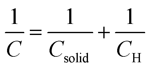 | (3) |
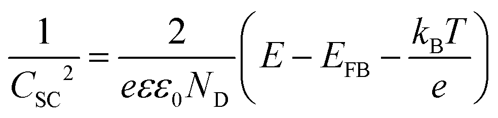 | (4) |
In this context, to apply eqn (4), the electrode should sustain a built-in potential, which requires the building blocks constituting the electrodes to be large enough. Porosity can be corrected by considering the real surface area.57 However, in the literature we can find examples were electrochemical impedance spectroscopic (EIS) measurements have been employed to experimentally obtain the capacitance of nanoporous electrodes and determine ND, without considering that the real surface area might be orders of magnitude larger than the geometric one.58
Electronic structure of nanoporous electrodes: surface states and trap states
The behavior of nanoporous electrodes cannot be rationalized on the basis of the existence of a SCR. In this case, when the Fermi level (potential) is far below (above) the conduction band edge (CB), they are insulating; as it approaches the CB edge upon negative polarization, within a potential range the electrode exhibits a certain degree of conductivity, which allows for a homogeneous charging of the electrode and thus for a homogeneous shift of the Fermi level with respect to the CB, provided the band edges are pinned. The conductivity arises from the thermal excitation of electrons to the CB or other states near the CB, or even by hopping between different electronic states. This causes a homogeneous electron occupancy of band-gap states, levelling with the substrate potential. The Csolid can be related in this case with the intrinsic film capacitance or chemical capacitance (Cμ), which usually is much smaller than CH and dominates the final electrochemical behavior. Neglecting the contribution coming from the SEI, and assuming an ideally polarizable electrode in quasi-equilibrium with band edge pinning conditions, Cμ (per geometric unit area) can be defined as (eqn (5)):59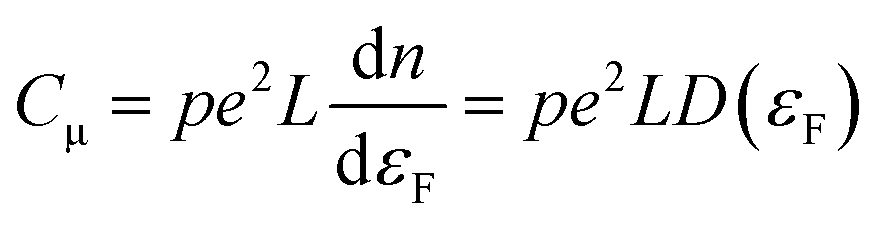 | (5) |
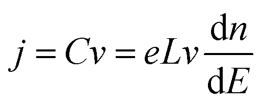
Bisquert and co-workers were the first to show the potentialities of cyclic voltammetry for this purpose.46,59–62 The capacitive currents measured can be ascribed as the filling/emptying of electronic states. The capacitive current density (j, A cm−2) relates the change of electron density with the change of electrode potential according to (eqn (6)):
 | (6) |
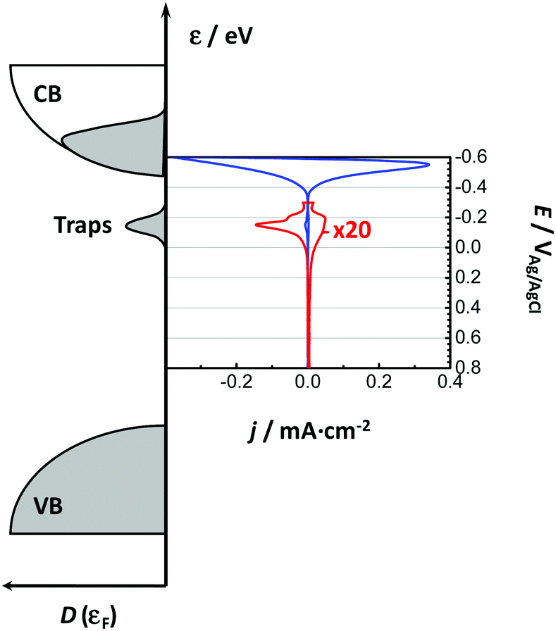 | ||
| Fig. 3 Scheme of the correlation between the cyclic voltammogram obtained in the dark in the absence of faradaic currents and the electronic density of states (DOS) for a nanoporous rutile electrode. VB and CB represent the valence and conduction band, respectively. The blue line corresponds to the filling/emptying of CB while the red line (intentionally magnified) refers to the filling/emptying of monoenergetic trap states at the grain boundaries. | ||
In line with the above ideas, we reviewed the variation of the capacitance with the potential for different locations of the electronic states.32,56 Considering eqn (5) and (6), and the theoretical DOS in the CB for an n-type SC, two limiting cases for the capacitance due to CB states can be obtained: (i) for a non-degenerated SC (eqn (7)):
 | (7) |
 | (8) |
![[thin space (1/6-em)]](https://www.rsc.org/images/entities/char_2009.gif) CCBμversus E, a straight line with a slope of (−e/kBT) is obtained, where the location of the CB can be estimated from the y-axis intercept.56
CCBμversus E, a straight line with a slope of (−e/kBT) is obtained, where the location of the CB can be estimated from the y-axis intercept.56
Considering now the intra-band gap states below the CB (i.e. surface states), at the zero-limit temperature, the corresponding capacitance can be estimated as (eqn (9)):46
 | (9) |
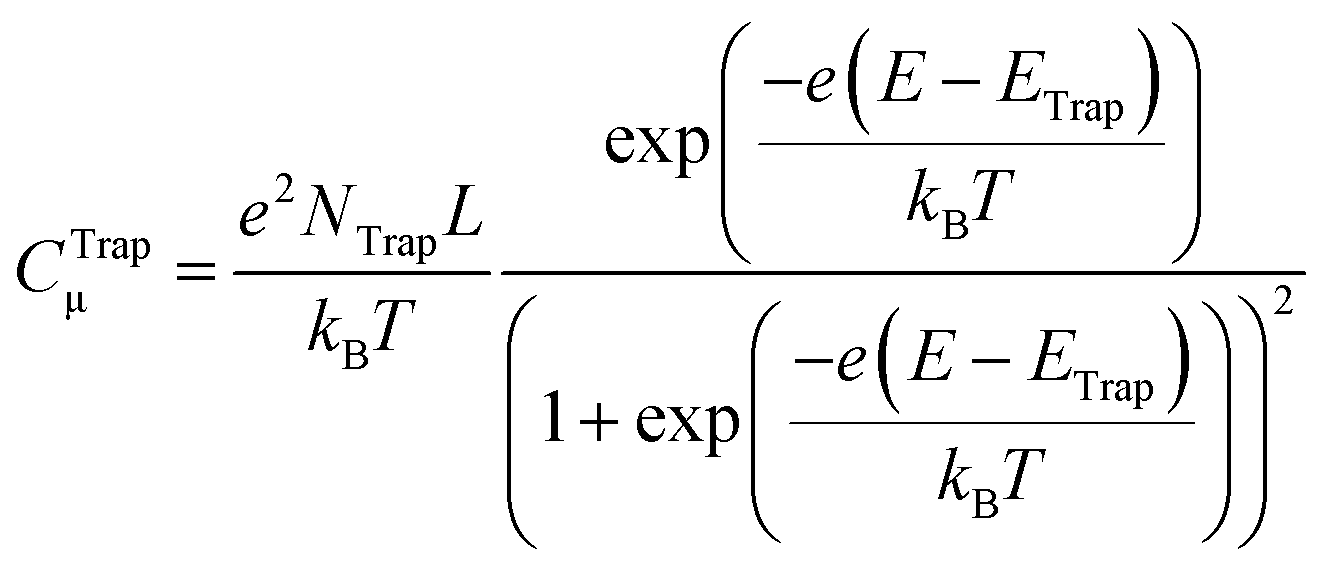 | (10) |
| Cμ = CCBμ + CSSμ + CTrapμ | (11) |
It is important to mention that to counterbalance the accumulated charge and preserve the electroneutrality of the material, ions are required. For example, when electrons are accumulated in TiO2, cations get adsorbed or inserted into the crystal structure, probably limited to the external layer exposed to the electrolyte. This fact can affect the direct quantitative interpretation of the electrochemical capacitance as a direct measurement of the DOS. Only in the case of electrodes with extremely small nanoparticles in which the electrolyte can easily permeate, the whole volume may accumulate charge.56 Such ion insertion has been evinced for different metal oxide SCs and it has been shown that it could be faster than the extraction one. Therefore, it is possible to take advantage of this process to promote their photocatalytic activity, as it causes a non-permanent electrochemical doping of the material.67,73,74
Furthermore, in the case of nanoporous electrodes, the voltammetric measurements in the dark can also be combined with open circuit photopotential decay measurements.75 Such a combination allows to evaluate the recombination and transfer (to solution) rate constants of charge carriers accumulated upon illumination at the metal oxide SC electrode. This evaluation is based on the fact that the integration of the voltammetric profile provides the actual charge carrier concentration in the nanostructured film as a function of the applied potential. As the photopotential decay curve displays the potential as a function of time, by a proper combination of both measurements the time evolution of the electron concentration is obtained, and hence the corresponding kinetic rate constants.75,76
Apart from the potential decay measurements, the currents under illumination (i.e. photocurrents) in the presence of electroactive species can also be employed to obtain further information about the energy location of the conduction band,56 the photocatalytic activity,69 the charge transfer rate and even, the reaction mechanism.39,77 In the case of TiO2, the electron donor species present in the electrolyte can be oxidized (i) indirectly, where the oxidation process occurs via surface trapped holes, also called hydroxyl radicals (by an isoenergetic interfacial hole transfer according to the Marcus–Gerischer energy model), or (ii) directly through its reaction with photogenerated VB free holes (by an inelastic interfacial hole transfer). By measuring the photocurrent as a function of the electron donor species concentration present in the electrolyte, it is possible to distinguish between both mechanisms.39,77 It is important to bear in mind that the electrochemical measurements suffer from the lack of specificity that can be surmounted by coupling them with spectroscopic measurements such as Raman or IR spectroscopy.78–83
Finally, it is worth mentioning that there exists a direct relationship between the appearance of capacitive currents in nanostructured TiO2 and WO3 electrodes and their electrocatalytic activity for cathodic processes in the dark. Our recent studies on CO2 reduction on these materials in acetonitrile solutions constitute clear examples of this behavior.84,85
Water photosplitting with metal oxides
Water photooxidation
The seminal work of Fujishima and Honda86 set the ground for using semiconductor metal oxides (i.e. TiO2) as photoelectrodes to sustain water oxidation in photoelectrocatalytic devices. Likewise, the works of Grätzel et al.23,87 with visible-sensitized mesoporous TiO2 as solar cells prompted the research on nanostructured materials. These breakthrough contributions inspired the experimental work on artificial photosynthesis that has continued to date. In this regard, the recent work on water photooxidation from the authors deals with the common topics in the field, including: materials, covering binary oxides (e.g. TiO2,56,70,88–91 WO3,92–94 and Fe2O357,91,96–98), hydroxides (Ni(OH)2)99–101 and ternary oxides (e.g. BiVO4,100–102 FeVO4,101 and TaON90); and modification strategies, such as doping,57,88,89,97,98 passivation,90,93,94 heterojunctions,91 compositing,89 surface modification,88,90,96 and the use of co-catalysts.95,99–101,103 In the following, we shall revise some of these works in terms of the modification strategy employed to improve the water photooxidation process (i.e. bulk modification and heterojunctions, surface modification, and the use of co-catalysts).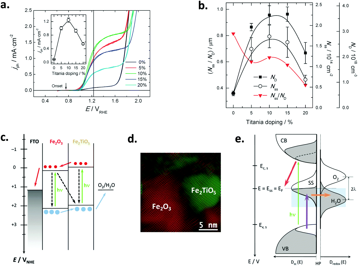 | ||
| Fig. 4 (a) Voltammetric measurements for hematite/titania electrodes under illumination with different titania doping; the vertical line depicts the thermodynamic potential value for the oxygen evolution reaction (1.23 VRHE); the inset shows the photocurrent density values at 1.23 VRHE as a function of titania doping. (b) Donor density (ND), total surface state density (Nss) and their ratio (Nss/ND) as a function of titania doping; ND was estimated from the slopes of the respective Mott–Schottky plots in the dark; Nss was obtained from integration of the density of surface states profiles, estimated from impedance measurements under illumination. (c) Thermodynamic scheme of the charge generation, transfer and recombination processes at the biased (1.23 VRHE) hematite/titania electrode under illumination, for intermediate and optimum titania doping values (5–15%). (d) HR-TEM micrograph of the hematite/titania 20% sample, shown as a coloured inverse FFT image highlighting the hematite (Fe2O3, red) and pseudo-brookite (Fe2TiO5, green) crystallographic phases. (e) Kinetic scheme of the charge generation and transfer processes at the biased (1.23 VRHE) hematite/titania-electrolyte interface under illumination, for the optimum titania doping values (10–15%). Reprinted with permission from ref. 91. Copyright 2015 The Royal Society of Chemistry. | ||
As for doping, recent work has been directed to the improvement of both binary and ternary oxides. In this way, Cots et al. have studied the doping of hematite with Mo,57,97 which was shown to be compatible with modification (surface passivation) with Yb.98 Quiñonero et al.100 attempted the improvement of bismuth vanadate photoanodes by means of La- or Ce-doping, and its subsequent surface modification with Au nanoparticles, as the bare material is recognized to suffer from slow charge transport and transfer rates at the SEI.106 With a 1 at% and 2 at% of La and Ce, water photooxidation was 2.3- and 4-times increased, respectively; this enhancement was probably due to the passivation of surface states, and the likeliness of lanthanum and cerium oxygenated species present at the surface that could yield a more negatively charged surface, as manifested by a negative shift on the flat band potential in both cases. Further modification with Au nanoparticles led to an enhanced photocurrent as they act as co-catalysts with no surface plasmon resonance effect, as shown from a direct comparison between the absorption spectra and the IPCE curves of the modified electrodes, in which no photocurrent arises in the plasmonic band region (ca. 580 nm). Interestingly, this double bulk-surface modification yields photoanodes that are potentially viable in bias-free tandem devices.
Another interesting dual bulk-surface modification example is that from Kim et al.90 where titania nanotube electrodes are both N-doped and surface modified with a TaON shell, which synergistically improves the photocurrent through an enhanced visible activity and a passivation of deleterious surface states induced by N-doping.
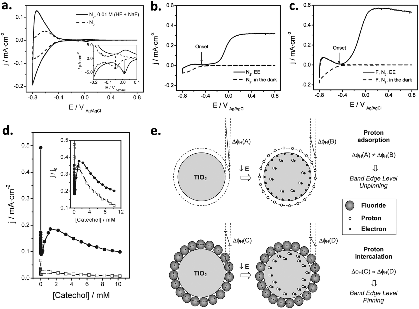 | ||
| Fig. 5 (a) Voltammograms in the dark of a nanoparticulate PI-KEM electrode (anatase + rutile 1:1), in the presence (solid line) and in the absence (dashed line) of 0.01 M (HF + NaF); the inset depicts the pair of peaks associated with grain boundaries. (b and c) Voltammograms in the dark (dashed line) and under polychromatic illumination (solid line) of a PI-KEM electrode similar to that shown in (a), in the absence (b) and in the presence (c) of 0.01 M (HF + NaF). (d) Stationary photocurrent density versus catechol concentration for a PI-KEM electrode, in the absence (open squares) and the presence (full circles) of 0.01 M (HF + NaF); the inset shows the normalized photocurrent density with respect to the photocurrent in the absence of catechol, corresponding to water photooxidation (j0). (e) Scheme depicting the predominant proton adsorption (top) or intercalation processes (bottom) on a titanium dioxide model particle, upon the application of a negative bias (E). The former process occurs in the absence of fluoride (band edge level unpinning), while the latter predominates in the presence of adsorbed fluoride (band edge level pinning). Reprinted with permission from ref. 88. Copyright 2011 American Chemical Society. | ||
In the dark, fluorination induces an increased capacitance in the accumulation potential region (Fig. 5a) for all TiO2 electrodes tested, due to the band edge level pinning phenomenon that favors proton insertion in the TiO2 particles without a significant change in the Helmholtz layer potential drop (Fig. 5e). On the contrary, the behavior under illumination is dependent on the TiO2 sample used and the substrate degraded. Fluorination increased the photocurrent for water (Fig. 5b and c) as well as for the oxidation of methanol, phenol and catechol (Fig. 5d), but decreased it for the oxidation of formic acid. The observed behavior could be rationalized in terms of the Direct–Indirect mechanism mentioned above.39,109 Substrates that do not strongly adsorb on titanium dioxide show a reduced recombination rate and an enhanced indirect oxidation rate by surface trapped holes (i.e. methanol, water). In contrast, those strongly chemisorbed show a diminished direct oxidation rate by valence band holes (i.e. formic acid), as fluorination displaces the substrates from the surface. In the case of phenol and catechol (Fig. 5d), fluoride prevents surface poisoning by oxidation intermediates, thus yielding enhanced photocurrents.
Another surface modifier that has been proven effective is trimethyl aluminum. In fact, hematite electrodes were shown to display an enhancement of the photoelectrochemical properties toward water oxidation upon modification.96 The effect was attributed to an improvement in charge carrier transport based on synchrotron radiation photoemission and X-ray absorption spectroscopy results.
Other examples of surface modification show an increased photoactivity, either through core–shell systems89 or conformal overlayers.93 In the former case, Kim et al.89 showed that compositing titania with graphene was beneficial for the degradation of pollutants and water oxidation, as graphene enhanced charge separation. In the latter case, Kim et al.93 uncovered, through voltammetric and transient spectroscopic measurements, the role of alumina overlayers on tungsten oxide as passivation layers for water photooxidation.
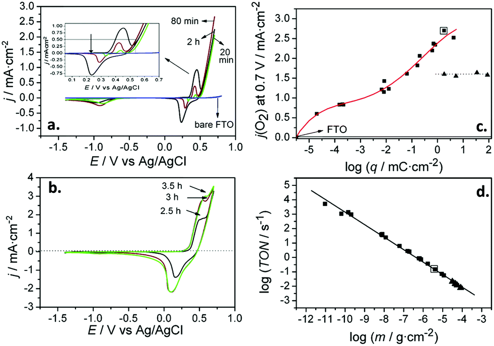 | ||
| Fig. 6 (a and b) Cyclic voltammograms for bare FTO (blue line) and FTO/Ni(OH)2 electrodes, corresponding to deposition times of (a) 20 min, 80 min and 2 h (green, red, and black lines, respectively) and (b) 2.5 h, 3 h and 3.5 h (black, red, and green lines, respectively). Inset in (a): Detail of the voltammetric curves in the high potential region. (c) Current density for the oxygen evolution reaction (OER) at 0.7 V for FTO/Ni(OH)2 electrodes versus the charge density for the reduction of NiOOH. (d) Turnover number (TON) for the OER at 0.7 V for FTO/Ni(OH)2 electrodes as a function of the Ni(OH)2 deposited mass per unit geometric surface area. Reprinted with permission from ref. 99. Copyright 2012 Hydrogen Energy Publications, LLC. Published by Elsevier Ltd. | ||
Subsequently, Quiñonero et al.101 optimized the amount of Ni(OH)2 to be deposited as OER co-catalyst on BiVO4 and FeVO4 photoanodes (Fig. 7). Using dark voltammetry, we were able to estimate the amount of deposited co-catalyst, showing that the photoactivity of the vanadate-based photoanodes reached an optimum with only 0.46 and 1.68 monolayers of Ni(OH)2 on BiVO4 and FeVO4, respectively (Fig. 7a and b); similar optimum monolayer amounts were required for La- and Ce-doped BiVO4 photoanodes. In all cases, the Ni(IV) species were the actual electrocatalytic centers, generated upon a successive 2 hole capture by Ni(II); then, Ni(IV) species transfer the holes to oxidize water, catalytically re-generating Ni(II) species on the surface (Fig. 7c). In this line, Jeon et al.95 have very recently published an example of a catalytic cycle mediated by Ag(I) species adsorbed on a WO3 photoanode, acting as a hole scavenger species that upon illumination reversibly transferred the photogenerated hole to water, re-generating Ag(I) in a continuous redox cycle, only limited by the photoreduction of Ag(I) to Ag(0).
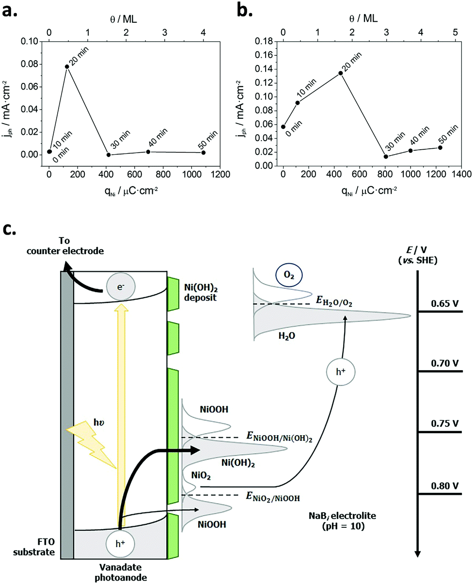 | ||
| Fig. 7 (a) Photocurrent density for the oxygen evolution reaction (OER) at −0.5 V for BiVO4/Ni(OH)2 photoanodes, prepared with different Ni(OH)2 deposition times (0–50 min) versus the charge density corresponding to the reduction of NiOOH (qNi) and the Ni(OH)2 coverage (θ) on the electrode surface. (b) Photocurrent density for the OER at 0.1 V for FeVO4/Ni(OH)2 photoanodes, prepared with different Ni(OH)2 deposition times (0–50 min) vs. qNi and θ. (c) Diagram for the mechanism through which the Ni(OH)2 deposit acts as a co-catalyst for the OER. Reprinted with permission from ref. 101. Copyright 2017 Elsevier B. V. | ||
To conclude, we will discuss the work of Recatalá et al.103 who prepared molybdenum sulfide clusters (Mo3S7) from the respective Mo complexes adsorbed on titanium dioxide; upon illumination, this hybrid system was reduced to generate Mo3S7, which subsequently acted as HER co-catalyst. This system showed a reduced overpotential for hydrogen evolution (up to 300 mV for 1 mA cm−2), and a significant increase of the hydrogen photogenerated in the presence of sacrificial hole scavengers (i.e. sulfide and sulfite). From a practical perspective, this system represents a simple and controlled modification method that could be used with other materials.
Water photoreduction
In the context of water splitting with metal oxides, (including those with a complex stoichiometry, i.e. ternary oxides), reports on photocathodes are much scarcer than those dealing with photoanodes. In principle, metal oxide photocathodes are advantageous as compared to traditional III–V or II–VI semiconductors (e.g. GaAs or CdS) as they tend to be more stable in the dark, cost-effective, and available (usually made of common metals).25 However, promising p-type metal oxides generally have a tendency to photocorrode in aqueous environments,25 which limits their practical application. Therefore, significant efforts in the last years have been devoted to finding low band gap, stable and efficient metal oxide photocathodes, engineered with strategies such as nanostructuring, formation of heterojunctions, deposition of protective layers or loading of co-catalyts.111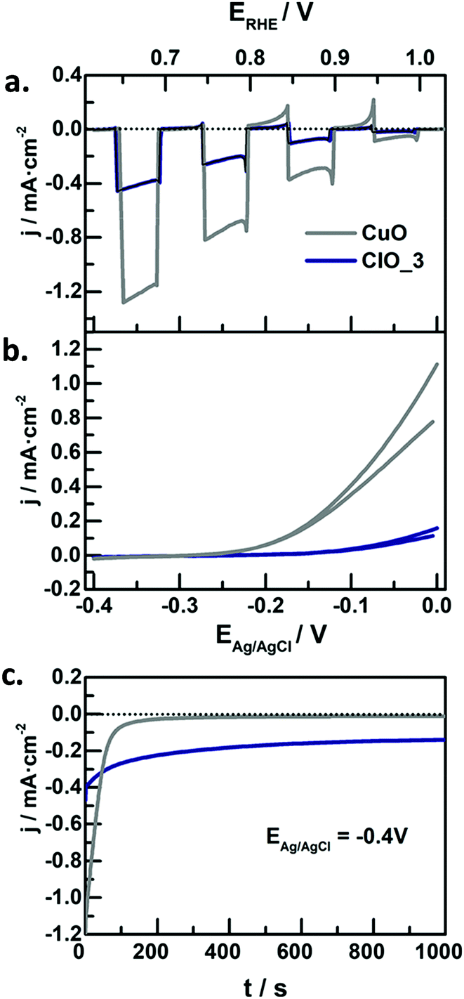 | ||
| Fig. 8 (a) Linear sweep voltammetry under transient illumination, (b) cyclic voltammograms in the dark, and (c) photocurrent at −0.4 V vs. Ag/AgCl for CuO (grey lines) and Fe-modified CuO (blue lines) electrodes in N2-purged 1 M NaOH. Illumination source: 320 mW cm−2, λ > 350 nm. Reprinted with permission from ref. 117. Copyright 2018 American Chemical Society. | ||
On the other hand, ternary oxides comprise a wide number of promising materials, such as spinels, delafossites, perovskites, scheelites and other families, which could potentially fulfill the requirements for light absorption, stability and photoactivity for solar hydrogen generation. Among them, CuBi2O4 has attracted considerable interest,118–120 reaching relatively high photocurrents, although instability under illumination has also been reported.121
In this context, CuFe2O4 spinel stands out because of its non-toxicity, environmental benignity and its composition based on Cu and Fe, which are earth-abundant elements. In this regard, we have prepared nanostructured spinel films by doctor blading a paste of commercial nanoparticles (30 nm in diameter).122 The bare electrodes presented small anodic photocurrents. However, once subjected to an oxidative electrochemical treatment (i.e. multiple voltammetric cycles up to a sufficiently positive potential, concretely, 1.6 VRHE in basic media), the photoelectrode character shifted to p-type, with an enhanced photoresponse. We hypothesized that the electrochemical treatment induces the formation of acceptor species in the solid. This strategy could open up new prospects for the formation of self-dopant species within metal oxide structures. From a practical perspective, as the photocurrent onset potential of the modified electrode was located at 1.1 VRHE, a rather positive value, it is feasible to combine CuFe2O4 with an n-type material in a tandem PEC device. In a similar way, Park et al.123 developed a flame-annealing method to synthesize CuFe2O4 electrodes with a low density of oxygen vacancies, reaching photocurrents exceeding all the previously reported values. However, the stability issue still needs to be addressed for the practical use of this oxide.
Another interesting group of materials is constituted by Cu(I) delafossites, which have been studied as transparent conductive oxides (TCOs) for optoelectronic devices,124 as they generally exhibit high carrier mobility and transparency. Among the delafossite family, CuFeO2 should be highlighted owing to its narrow band gap (1.5 eV), being the most studied delafossite in the context of water splitting.125–128 Despite its generally good stability in aqueous environments, the photocurrents in the absence of O2 (as electron scavenger) are very low. It has been reported that Fermi level pinning linked to the Fe3+/Fe2+ couple hinders the HER reaction in this material.129,130 Remarkably, NiFe an CoFe layered double hydroxides (LDHs) co-catalysts on CuFeO2 have led to major improvements in the photoresponse.127,128 Díaz-García et al.131 studied thin transparent CuCrO2 films as photocathodes for water splitting synthesized by a simple sol–gel method. In contrast with CuFeO2, the as-prepared bare electrodes already showed a relatively high IPCE (6% at 350 nm) for proton reduction with a rather positive photocurrent onset potential and remarkable photostability in both acidic and alkaline media. In view of the outstanding photoelectrochemical properties of this material, increasing its visible light absorption (for instance, by doping) seems imperative for its potential solar application, as the pristine material has a band gap of 3.15 eV.
Iron perovskites have been also investigated for water splitting, including BiFeO3,132,133 YFeO3,134 and LaFeO3, being the latter the most studied. Lanthanum iron perovskite electrodes can exhibit both photoanodic or photocathodic behavior, depending on the synthetic route and conditions.135–138 We have reported a straightforward wet chemical method to synthesize p-type thin film LaFeO3 electrodes.137 By introducing Mg or Zn as dopants, the p-type character is enhanced. For a LaFe0.95M0.05O3 (M = Mg or Zn) stoichiometry, a 6-fold increase of the photocurrent is attained in the presence of O2 with respect to the pristine material (Fig. 9a and b). This effect is attributed to the substitution of trivalent Fe atoms by divalent Mg and Zn atoms in the perovskite lattice, which likely induces: (i) an increase of the Fe4+ density, and (ii) an improvement of carrier mobility due to lattice distortion. Impedance spectroscopy analysis through Mott–Schottky and Nyquist plots confirmed an increase in both charge carrier density and conductivity. Doping with equivalent quantities of either Mg or Zn led to similar photocurrent values, suggesting that both cations produce similar effects within the perovskite structure (Fig. 9).
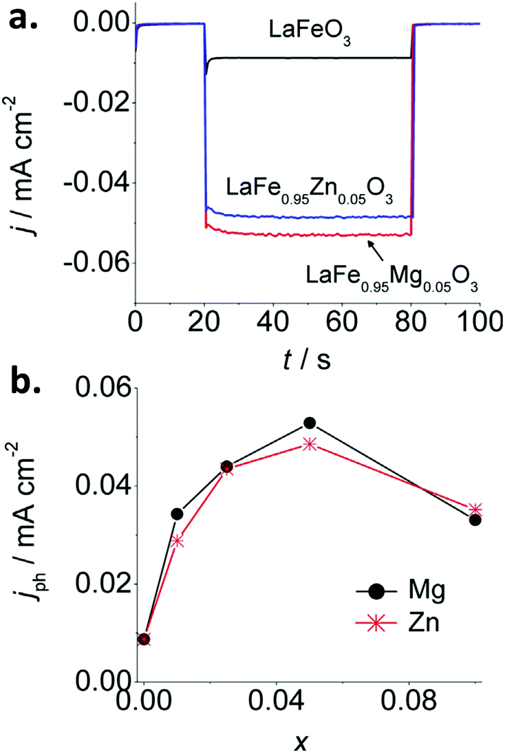 | ||
| Fig. 9 (a) Photocurrent transients at −0.25 V vs. Ag/AgCl for pristine LaFeO3 and doped LaFe1−xMxO3 (M = Mg or Zn) with x = 0.05 and (b) stationary photocurrent at −0.25 V vs. Ag/AgCl after 60 s of illumination as a function of x in LaFe1−xMxO3 (M = Mg or Zn) electrodes in O2-purged 0.1 M NaOH. Reprinted with permission from ref. 137. Copyright 2017 Wiley-VCH Verlag GmbH & Co. | ||
Traditionally, these studies have focused on n-type oxide materials, but they can be easily extended to p-type SCs. For instance, Ponomarev et al.142 investigated p-InP electrodes only by appropriate sign reversal of a model valid for n-type photoelectrodes. Later on, some of us143 used the model developed by Leng et al.144 for n-TiO2 to study p-CaFe2O4 photocathodes (Fig. 10a). Electrons were considered as minority carriers, and the HER mechanism taken into account (Fig. 10b). For the first time, as far as we know, a kinetic model (without using equivalent circuits) was employed to describe the SEI at an illuminated metal oxide photocathode. A remarkable good fit of the experimental data (in both Nyquist and Bode plots, Fig. 10c) was achieved. The following mechanism was assumed (Fig. 10b): (i) electrons in the conduction band can be trapped at surface states or be transferred to the electrolyte, (ii) recombination can take place in the bulk and via surface states, and (iii) electron transfer to the electrolyte likely occurs from the conduction band rather than from surface states. Both recombination and charge transfer kinetic constants were observed to depend on the applied potential, suggesting that an intermediate situation between Fermi level pinning and band edge pinning prevails at the SEI. In addition, it was also demonstrated that most of the photogenerated charge carriers recombine in the SC bulk.
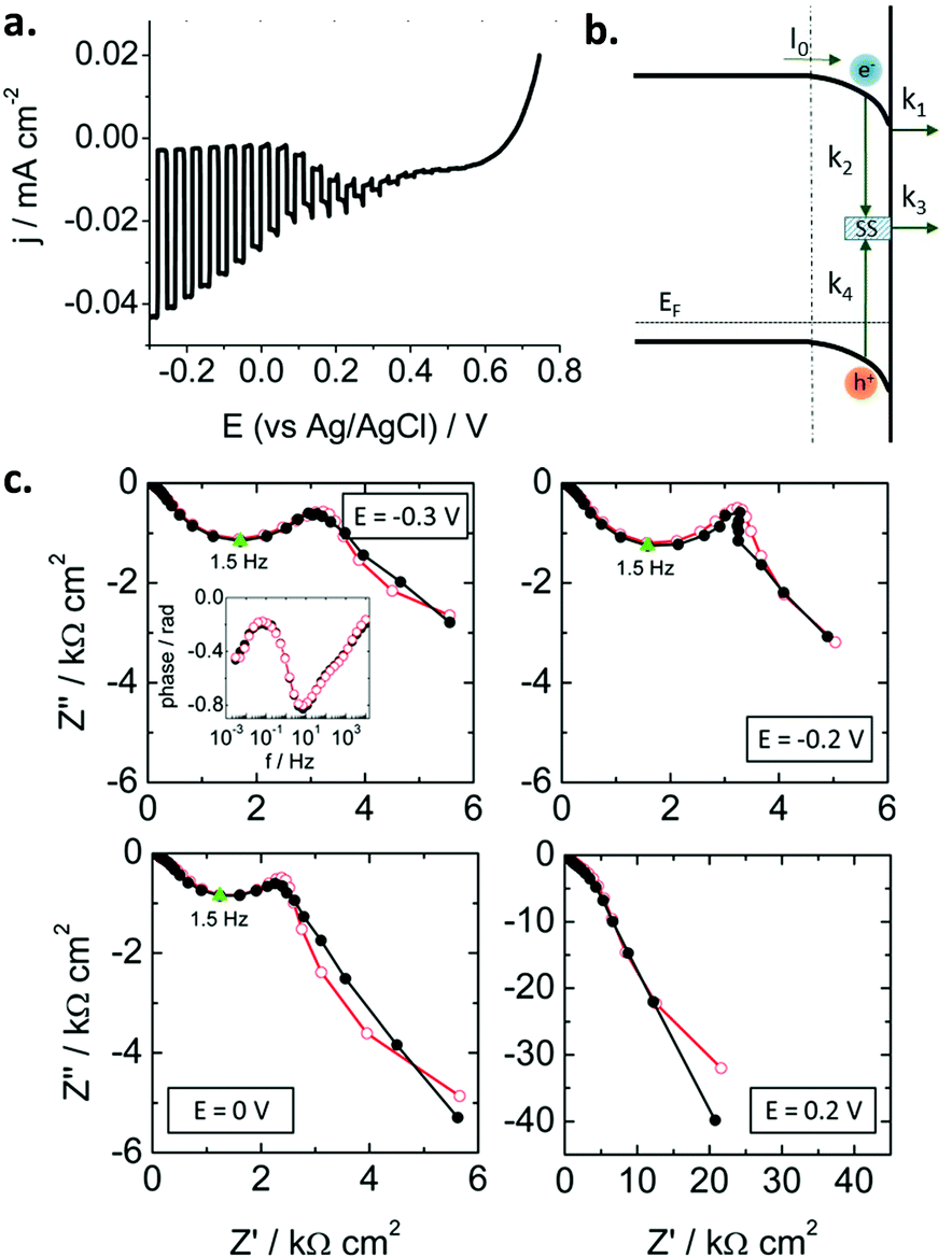 | ||
| Fig. 10 (a) Linear sweep voltammogram under transient illumination for a calcium ferrite electrode. (b) Scheme illustrating the different charge transfer processes at the p-type semiconductor–electrolyte interface (SEI). (c) Nyquist plots under illumination for different potentials showing experimental points (black solid symbols) and simulated curves (red open symbols). Points corresponding to ωmax are marked in green. Inset: Experimental and simulated Bode plots at −0.3 V. Illumination: 93 mW cm−2, AM 1.5G. Electrolyte: N2-purged 0.1 M Na2SO4. Reprinted with permission from ref. 143. Copyright 2016 American Chemical Society. | ||
Tandem processes and modeling
As discussed above, the fact that the oxides can be employed for both cathodic and anodic processes in artificial photosynthesis, including water photosplitting, makes feasible to devise all-oxide-based photosynthetic devices. Fig. 11 illustrates the three modalities in which artificial photosynthesis can occur in the case of systems formed by nanoparticles of oxides immersed in an aqueous medium. We have, on the one hand, the system consisting of a single semiconductor oxide (Fig. 11, left). It is very difficult to find a material that produces the photoelectrolysis of water with reasonable efficiency in this case, since it is necessary that: (i) both the CB and VB edges straddle the levels corresponding to the redox pairs H2O/H2 and O2/H2O, and (ii) the band gap is narrow enough as to enable efficient sunlight harvesting. In addition, it should be noted that there must be some extra driving force for the transfer of charge carriers to occur (because of the existence of significant overpotentials, particularly for water oxidation). In contrast, the realization of artificial photosynthesis in two stages makes it possible to obtain greater efficiencies and multiplies the possibility of finding more promising systems since two photoactive materials are now combined. In this case, oxidation and reduction photoreactions occur in separate materials whose p- or n-type characteristics and the position of their bands have been optimized to perform one of the half-reactions. In addition, having the two redox processes spatially separated enables the search of specific co-catalysts for both anodic and cathodic reactions.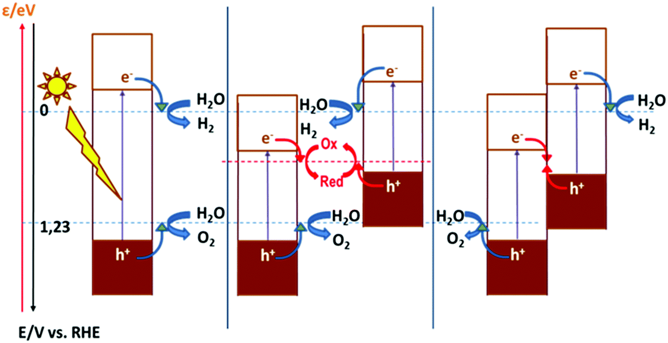 | ||
| Fig. 11 Band diagrams and redox processes involved in the photoelectrolysis of water for systems consisting of a single photoactive material (one stage, left) and two photoactive materials in the presence of a redox mediator (center) or by direct contact (right). | ||
As observed, in the case of systems consisting of dispersed semiconductor particles, there are two possibilities to combine the two photoactive materials. First, a reversible redox pair whose level must be between the CB edge of the material that supports photooxidation and the VB edge of the material supporting photoreduction (Fig. 11, center) can be employed. Secondly, the direct particle junction of the two photoactive materials could be envisaged (Fig. 11, right). Among the oxides commonly employed for water oxidation, one finds TiO2, WO3, Fe2O3, BiVO4, ZnO, CoOx, CoTiO3, LaFeO3, BiOx and oxides with more complex stoichiometries based on Bi and either Ta or Nb. The choice of oxides for sustaining water reduction is much more limited, being SrTiO3 with an appropriate co-catalyst, the most typical.145,146
The concepts presented above for a dispersed particle system can be easily extended to photoelectrochemical cells. Fig. 12 illustrates the functioning of photoelectrolysis cells based on a photoanode + dark cathode (Fig. 12, one stage left), a photocathode + dark anode (Fig. 12, one stage right), and a photoanode + photocathode combination (Fig. 12, left). The latter are made up of two photoelectrodes: one n-type, which works as a photoanode and another p-type, which acts as a photocathode. This is the way in which the so-called tandem cells are constructed. In tandem cells, both electrodes are photoexcited by the same light beam. This is achieved with photoelectrodes whose light absorption is complementary. The light passes first through the wide band gap material and subsequently, it is absorbed by the narrow band gap material. Obviously, the electrolyte solution separating the electrodes could absorb part of the light, causing efficiency to decrease. One could conceive photoelectrochemical cells with two photoelectrodes that are illuminated in parallel rather than in series. These are also considered by many authors as tandem cells.147
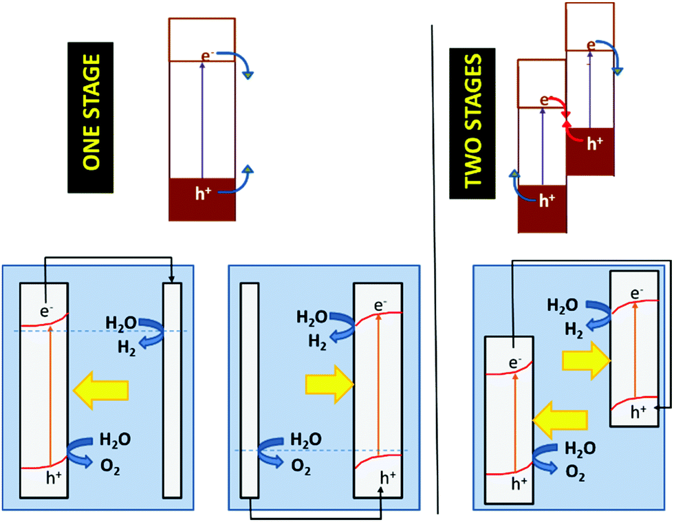 | ||
| Fig. 12 A schematic illustrating the photoelectrochemical variants of artificial photosynthesis systems in one and two stages. In the case of the one-stage system, the photoelectrode could sustain either the oxidation (photoanode) or reduction (photocathode) process, while the other half-reaction is performed by a conventional non-photoactive electrode (cathode or anode, respectively). In the case of the two-stage system, where a photoanode and a photocathode are connected in series, the electrochemical device is known as a tandem cell. | ||
It is well-known that developing tandem cells for solar fuel generation may benefit from the facts that: (i) it is more likely to find a pair of photoelectrodes whose band edges are located at the appropriate energies to carry out water photooxidation and water or CO2 photoreduction than to identify a single photoactive material; (ii) it is easier to find specific co-catalysts for each of the redox processes so that there is no interference between them; and (iii) the maximum theoretical efficiency that can be achieved is larger than in cells with a single photoelectrode.148,149
Lately, we have been devoting a significant effort for the clarification of the factors that influence the solar-to-hydrogen (STH) conversion efficiency either under zero-bias conditions or under applied bias (Applied bias photo-to-current efficiency, ABPE, for hydrogen generation). Although this question has been dealt with in several papers, a quasi-analytical approach based on the classical Gärtner model has not been reported yet.
We have recently embarked on such a project. It is instructive to show that the ABPE (or the STH efficiency) may substantially differ from the maximum value calculated on the basis of electrode band gaps because of different properties that are central in the field, such as, for instance, the diffusion length of the minority carrier, the separation of photocathode and photoanode flat band potentials, the absorption coefficients, or the doping density. The electronic structure of oxides is characterized by a weak curvature of the energy vs. momentum curve, leading to large effective masses for the charge carriers and thus, to short diffusions lengths. This is particularly critical for the minority carriers. Thus, efficiency calculations are pertinent as the photoelectrochemical behavior is most of the times far away from ideal, limiting the usefulness of typical theoretical studies. It is worth noting that recent studies have attempted to address this question, at least partially.149,150 In our model we have neglected mass transport limitations and light absorption by the electrolyte, while the behavior of both electrodes has been considered to follow the ideas delineated by Gärtner, either for front-side or back-side illumination. Light absorption is considered to follow a simple model (Tauc relationship). In addition, surface recombination and carrier transfer constants are considered in an explicit way.
To illustrate the potential usefulness of this type of calculations, Fig. 13 shows a set of ABPE curves as a function of the applied bias (V) for different values of the doping density (Fig. 13a), minority carrier diffusion length (Fig. 13b), absorption coefficients (Fig. 13c) and difference between flat band potentials of photocathode and photoanode (Fig. 13d). All these properties refer to the photoanode (wide band gap material). As observed, relatively high values for the conversion efficiency can be attained for the reference scenario with substantial surface recombination and a fixed photocathode. The effect of the parameters mentioned above on the maximum ABPE is dramatic, particularly in the case of the absorption coefficient and the minority carrier diffusion length. In any case, this type of calculations should be useful for guiding the choice of the most promising materials taking into account the intrinsic non-ideality of practical oxide electrodes.
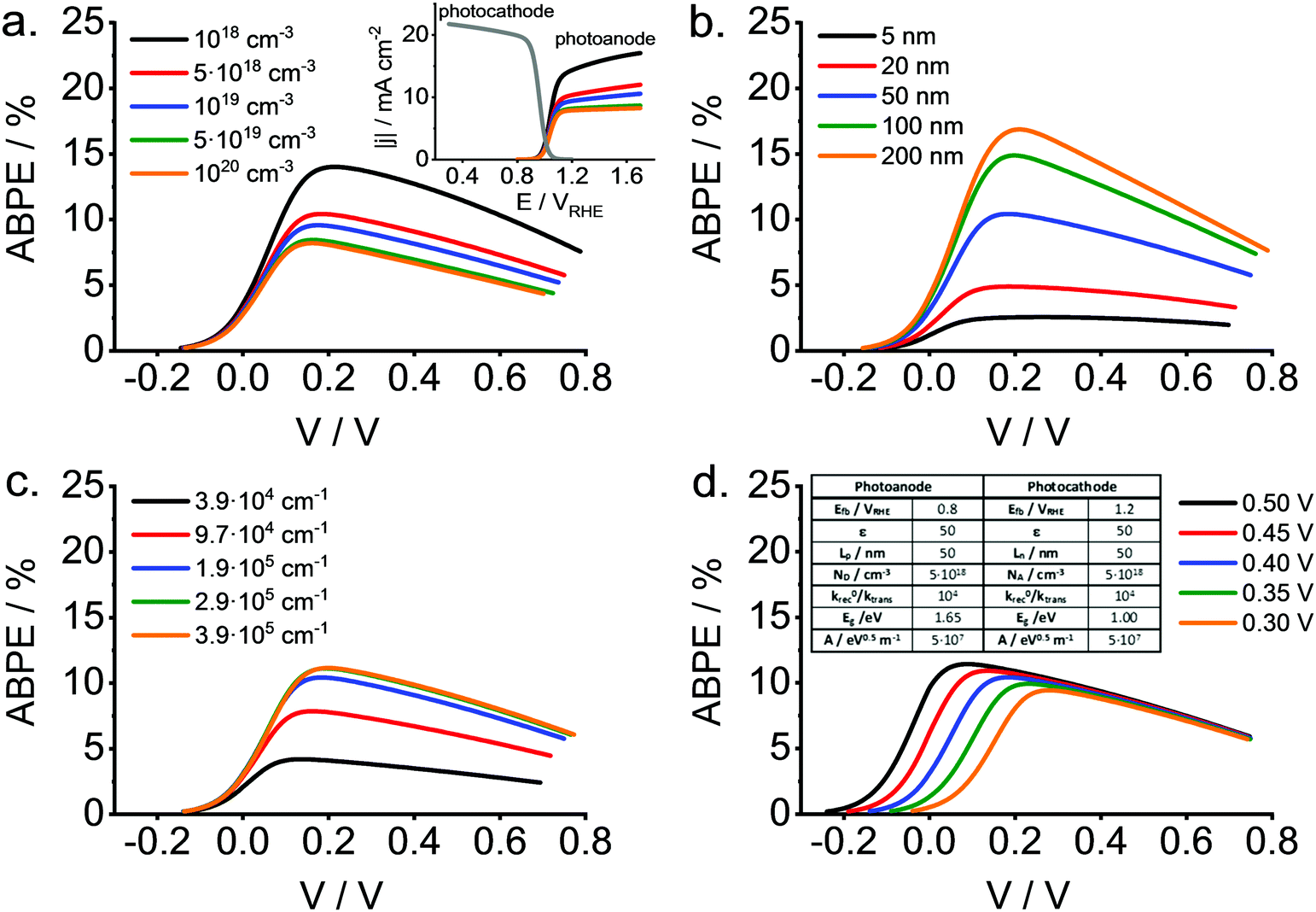 | ||
| Fig. 13 ABPE vs. bias (V) curves of a tandem cell for different values of the photoanode properties, including: (a) doping density, ND; (b) minority carrier diffusion length, Lp; (c) absorption coefficient values at 400 nm (assuming direct band gap and Tauc equation: αhν = A(hν − Eg)0.5, for different values of A ranging from 107 to 108 eV0.5 m−1); and (d) difference between the flat band potential for the photocathode and the photoanode. Inset in (d) shows the model parameters used in the calculation, being the photoanode thickness of 100 nm. Inset in (a) displays photocurrent (absolute values) as a function of potential for both photocathode and photoanode (for different doping densities). | ||
Together with the problem of low efficiencies, what makes it difficult to develop devices is to find semiconductor electrode materials presenting enough stability in contact with the typical either acid or alkaline aqueous media. Oxides will tend to be more stable in an aqueous environment than semiconductors such as chalcogenides. In fact, some photoanode materials have enough stability in acid (e.g. WO3) or alkaline (e.g. Fe2O3) environments. However, the challenge of finding efficient and stable p-type oxide electrodes still needs to be addressed.
A direction to palliate the stability problem could be based on alternative photoelectrolyzer designs. In this respect, it is particularly interesting to advance toward the development of quasi-solid-sate devices in which the liquid electrolyte is substituted by a polymer electrolyte membrane. Recent results obtained in our laboratory in collaboration with Aricò's laboratory (ITAE-CNR, Italy) show that this option is feasible by working with a tandem device based on a hematite photoanode and a CuO photocathode. Photoresponses like those obtained in a conventional liquid electrolyte were obtained, but with a greater stability of the semiconductor electrodes.151,152 This is particularly important in the case of the photocathode, which is prone to severe photocorrosion, except for some delafossites, as mentioned above.126,129,131
Although significant progress has been made in the last years, the development of practical water splitting (artificial photosynthesis) photoelectrochemical devices requires additional effort. Both the conversion efficiency and the stability of the photoelectrodes need to be addressed, considering that they scale differently with the band gap. Increasing the conversion efficiency will depend on finding oxides with narrow band gap and appropriately engineered bulk and surface properties promoting carrier mobility and transfer to the electrolyte. For increasing stability, three compatible directions could be explored: (i) finding new materials (ternary or multinary oxides); (ii) identifying appropriate means of protecting the electrode surface, including the use of co-catalysts; and (iii) substituting the conventional liquid electrolytes by polymer electrolytes. The latter will bring about new device designs closer to the flat configuration desirable for the mass deployment of this technology.
Conclusions and outlook
In recent years there has been a tremendous effort to develop new electrode materials based on transition metal oxides. However, there are many aspects that still need to be improved to enable their use in devices converting solar energy into chemical energy or in environmental applications. The Achilles’ heels of these materials are their sometimes low stability in contact with aqueous media under illumination as well as their low conversion efficiency.The stability of oxides is generally better than that of other semiconductors (e.g. chalcogenides), and some of them show a satisfactory photostability for many applications (e.g. titanium dioxide, tungsten trioxide and hematite); however, durability should be improved in the cost-effective copper-based binary and ternary oxides, which commonly have a clear tendency to photocorrode. Thus, work to stabilize these materials is still needed. In relation to the low conversion efficiency, methods that modify both the bulk and the surface of the semiconductor electrodes should be considered, facilitating the mobility of carriers and decreasing recombination both in the bulk and on the surface. It is worth noting that a simple strategy to improve both stability and conversion efficiency is based on nanostructuring the electrode materials. The preparation of structures ordered at the nanoscopic level with quasi-one-dimensional objects (e.g. nanocolumns, nanorods or nanofibers) is especially interesting, provided the nanoobject diameter can be tuned to make compatible an extended interfacial area with the existence of a space charge region in the electrodes, which certainly enhances charge separation and decreases recombination within the semiconductor.
The experimental work required to achieve efficient and stable oxide electrodes should be guided (both in their a priori orientation and a posteriori rationalization) by theoretical physicochemical methods for, among others: (i) the selection of new oxide materials as potential candidates in the photoelectrochemical processes of interest; (ii) the extraction of microscopic information on the kinetics of the different electrode processes occurring under illumination; (iii) the interpretation of the experimental results with kinetic models; and (iv) the development of suitable devices to carry out artificial photosynthesis. Regarding the materials, there are many ternary and multinary metal oxides that are yet to be explored; the enormous number of candidates advises the use of DFT calculations to filter them down to an initial selection that serves as a starting point for further experimental work. Regarding the devices, models should comprise transport phenomena (both in the electrolyte and the semiconductor), besides the material and kinetic aspects of the photoinduced charge transfer phenomena.
Finally, as a prospective outlook for the future research with metal oxides as photoelectrocatalysts, we propose here a succinct guideline to each of the issues mentioned above. Regarding materials stability, the use of protective layers (made of materials fully stable in aqueous media) should be explored in the future, but with greater emphasis on cost efficiency and scalability than up to now; moreover, the use of co-catalysts that channel the transfer to solution of minority carriers is a method of improving stability and additional efforts should be made in this direction. As for their low efficiency, protective layers can promote increased conversion efficiency by allowing selective transport of minority carriers, while blocking that of majority carriers. In any case, the use of co-catalysts and doping will be of particular importance.
Concerning the modeling of materials, DFT calculations will provide reliable electronic structures for the oxides. We expect that, in the coming years, the number and quality of publications on oxide electronic structures and on the electronic and optical properties derived therefrom will increase. This approach will also be useful for optimizing photoactivity improvement strategies, such as doping. On the other hand, kinetic modeling should allow the identification of the limiting steps under operation and it is therefore especially useful to unravel all the information provided by the electrochemical methods resolved in the frequency or time domains. Finally, at the device level, the theoretical studies should guide the cell design, having in mind the potential up-scaling and marketing, while helping to improve the conversion efficiency and especially the stability of the photoelectrodes. In this sense, the development of tandem photoelectrochemical cells based on polymeric electrolyte membranes can be a pathway for designing durable and scalable devices.
All in all, we believe that in the near future new opportunities will continue to appear for researchers who are currently working on these issues as well as for newcomers wanting to join the exciting challenge of achieving conversion and storage of solar energy in a cost-effective and environmentally benign way. There is no doubt that in the coming years, efforts will concentrate in this direction, to contribute to the de-carbonization of our energy system and our economy. The multidisciplinary approach that we have illustrated in this contribution can hopefully serve as an inspiration for the emergence of new and promising ideas.
Conflicts of interest
There are no conflicts to declare.Acknowledgements
Continued support from the Spanish Ministry of Science and Innovation (MICINN) is gratefully acknowledged, in particular through the current project RTI2018-102061-B-I00 (FONDOS FEDER). Financial support from the Generalitat Valenciana through project PROMETEO/2020/089 is also thanked. Finally, we are also grateful to our many collaborators during the last 15 years, who also made this contribution possible.Notes and references
- N. S. Lewis and D. G. Nocera, Proc. Natl. Acad. Sci. U. S. A., 2006, 103, 15729–15735 Search PubMed.
- D. G. Nocera, Acc. Chem. Res., 2017, 50, 616–619 Search PubMed.
- A. J. Bard, J. Photochem., 1979, 10, 59–75 Search PubMed.
- K. Rajeshwar, A. Thomas and C. Janaky, J. Phys. Chem. Lett., 2015, 6, 139–147 Search PubMed.
- M. Anne Fox and A. J. Bard, Acc. Chem. Res., 1995, 28, 141–145 Search PubMed.
- F. E. Osterloh, ACS Energy Lett., 2017, 2, 445–453 Search PubMed.
- K. Rajeshwar, J. Phys. Chem. Lett., 2011, 2, 1301–1309 Search PubMed.
- H. Kisch, Angew. Chem., Int. Ed., 2013, 52, 812–847 Search PubMed.
- S. E. Braslavsky, A. M. Braun, A. E. Cassano, A. V. Emeline, M. I. Litter, L. Palmisano, V. N. Parmon and N. Serpone, Pure Appl. Chem., 2011, 83, 931–1014 Search PubMed.
- H. Park, H. Il Kim, G. H. Moon and W. Choi, Energy Environ. Sci., 2016, 9, 411–433 Search PubMed.
- B. Ohtani, J. Photochem. Photobiol., C, 2010, 11, 157–178 Search PubMed.
- B. Ohtani, Phys. Chem. Chem. Phys., 2014, 16, 1788–1797 Search PubMed.
- J. Yang, D. Wang, H. Han and C. Li, Acc. Chem. Res., 2013, 46, 1900–1909 Search PubMed.
- P. Lianos, Appl. Catal., B, 2017, 210, 235–254 Search PubMed.
- K. Sivula and R. Van De Krol, Nat. Rev. Mater., 2016, 1, 15010 Search PubMed.
- A. Hankin, F. E. Bedoya-Lora, C. K. Ong, J. C. Alexander, F. Petter and G. H. Kelsall, Energy Environ. Sci., 2017, 10, 346–360 Search PubMed.
- J. Li and N. Wu, Catal. Sci. Technol., 2015, 5, 1360–1384 Search PubMed.
- Y. Yang, S. Niu, D. Han, T. Liu, G. Wang and Y. Li, Adv. Energy Mater., 2017, 7, 1–26 Search PubMed.
- C. Jiang, S. J. A. Moniz, A. Wang, T. Zhang and J. Tang, Chem. Soc. Rev., 2017, 46, 4645–4660 Search PubMed.
- K. Sivula, J. Phys. Chem. Lett., 2013, 4, 1624–1633 Search PubMed.
- S. Jung, C. C. L. McCrory, I. M. Ferrer, J. C. Peters and T. F. Jaramillo, J. Mater. Chem. A, 2016, 4, 3068–3076 Search PubMed.
- F. Song, L. Bai, A. Moysiadou, S. Lee, C. Hu, L. Liardet and X. Hu, J. Am. Chem. Soc., 2018, 140, 7748–7759 Search PubMed.
- F. E. Osterloh, Chem. Soc. Rev., 2013, 42, 2294–2320 Search PubMed.
- S. Chen, S. S. Thind and A. Chen, Electrochem. Commun., 2016, 63, 10–17 Search PubMed.
- I. Sullivan, B. Zoellner and P. A. Maggard, Chem. Mater., 2016, 28, 5999–6016 Search PubMed.
- N. K. Awad, E. A. Ashour and N. K. Allam, J. Renewable Sustainable Energy, 2014, 6, 022702 Search PubMed.
- Z. Haider, H. W. Yim, H. W. Lee and H. il Kim, Int. J. Hydrogen Energy, 2020, 45, 5793–5815 Search PubMed.
- Z. Chen, T. F. Jaramillo, T. G. Deutsch, A. Kleiman-Shwarsctein, A. J. Forman, N. Gaillard, R. Garland, K. Takanabe, C. Heske, M. Sunkara, E. W. McFarland, K. Domen, E. L. Milled and H. N. Dinh, J. Mater. Res., 2010, 25, 3–16 Search PubMed.
- H. Dotan, K. Sivula, M. Grätzel, A. Rothschild and S. C. Warren, Energy Environ. Sci., 2011, 4, 958–964 Search PubMed.
- X. Zhao, W. Luo, J. Feng, M. Li, Z. Li, T. Yu and Z. Zou, Adv. Energy Mater., 2014, 4, 1–7 Search PubMed.
- N. Guijarro, M. S. Prévot and K. Sivula, Phys. Chem. Chem. Phys., 2015, 17, 15655–15674 Search PubMed.
- T. Berger, D. Monllor-Satoca, M. Jankulovska, T. Lana-Villarreal and R. Gómez, ChemPhysChem, 2012, 13, 2824–2875 Search PubMed.
- S. Hennessey and P. Farràs, Chem. Commun., 2018, 54, 6662–6680 Search PubMed.
- L. M. Peter, Electroanalysis, 2015, 27, 864–871 Search PubMed.
- C. Janáky and K. Rajeshwar, ACS Energy Lett., 2017, 2, 1425–1428 Search PubMed.
- W. J. Yin, H. Tang, S. H. Wei, M. M. Al-Jassim, J. Turner and Y. Yan, Phys. Rev. B: Condens. Matter Mater. Phys., 2010, 82, 1–6 Search PubMed.
- M. Woodhouse and B. A. Parkinson, Chem. Soc. Rev., 2009, 38, 197–210 Search PubMed.
- H. Gerischer, J. Electroanal. Chem., 1975, 58, 263–274 Search PubMed.
- T. Lana Villarreal, R. Gómez, M. Neumann-Spallart, N. Alonso-Vante and P. Salvador, J. Phys. Chem. B, 2004, 108, 15172–15181 Search PubMed.
- W. W. Gärtner, Phys. Rev., 1959, 116, 84–87 Search PubMed.
- A. Hagfeldt, H. Lindström, S. Södergren and S. E. Lindquist, J. Electroanal. Chem., 1995, 381, 39–46 Search PubMed.
- P. V. Kamat, J. Phys. Chem. Lett., 2012, 3, 663–672 Search PubMed.
- P. V. Kamat, Acc. Chem. Res., 2017, 50, 527–531 Search PubMed.
- A. R. C. Bredar, A. L. Chown, A. R. Burton and B. H. Farnum, ACS Appl. Energy Mater., 2020, 3, 66–98 Search PubMed.
- F. Fabregat-Santiago, G. Garcia-Belmonte, J. Bisquert, A. Zaban and P. Salvador, J. Phys. Chem. B, 2002, 106, 334–339 Search PubMed.
- F. Fabregat-Santiago, I. Mora-Seró, G. Garcia-Belmonte and J. Bisquert, J. Phys. Chem. B, 2003, 107, 758–768 Search PubMed.
- Y. K. Gaudy and S. Haussener, J. Mater. Chem. A, 2016, 4, 3100–3114 Search PubMed.
- T. Shinagawa, Z. Cao, L. Cavallo and K. Takanabe, J. Energy Chem., 2017, 26, 259–269 Search PubMed.
- S. Hu, C. Xiang, S. Haussener, A. D. Berger and N. S. Lewis, Energy Environ. Sci., 2013, 6, 2984–2993 Search PubMed.
- P. C. K. Vesborg and B. Seger, Chem. Mater., 2016, 28, 8844–8850 Search PubMed.
- A. Solbrand, H. Lindström, H. Rensmo, A. Hagfeldt, S. E. Lindquist and S. Södergren, J. Phys. Chem. B, 1997, 101, 2514–2518 Search PubMed.
- A. Solbrand, A. Henningsson, S. Södergren, H. Lindström, A. Hagfeldt and S. E. Lindquist, J. Phys. Chem. B, 1999, 103, 1078–1083 Search PubMed.
- Y. Pleskov, Semiconductor Photoelectrochemistry, Springer, US, 1986 Search PubMed.
- N. Kopidakis, E. A. Schiff, N. G. Park, J. Van De Lagemaat and A. J. Frank, J. Phys. Chem. B, 2000, 104, 3930–3936 Search PubMed.
- T. Lana-Villarreal and R. Gómez, Chem. Phys. Lett., 2005, 414, 489–494 Search PubMed.
- M. Jankulovska, T. Berger, T. Lana-Villarreal and R. Gómez, Electrochim. Acta, 2012, 62, 172–180 Search PubMed.
- A. Cots, D. Cibrev, P. Bonete and R. Gómez, ChemElectroChem, 2017, 4, 585–593 Search PubMed.
- A. Hankin, F. E. Bedoya-Lora, J. C. Alexander, A. Regoutz and G. H. Kelsall, J. Mater. Chem. A, 2019, 7, 26162–26176 Search PubMed.
- J. Bisquert, Phys. Chem. Chem. Phys., 2003, 5, 5360–5364 Search PubMed.
- I. Abayev, A. Zaban, V. G. Kytin, A. A. Danilin, G. Garcia-Belmonte and J. Bisquert, J. Solid State Electrochem., 2007, 11, 647–653 Search PubMed.
- J. Bisquert, Phys. Chem. Chem. Phys., 2008, 10, 49–72 Search PubMed.
- J. Bisquert, F. Fabregat-Santiago, I. Mora-Seró, G. Garcia-Belmonte, E. M. Barea and E. Palomares, Inorg. Chim. Acta, 2008, 361, 684–698 Search PubMed.
- J. Bisquert and V. S. Vikhrenko, J. Phys. Chem. B, 2004, 108, 2313–2322 Search PubMed.
- H. Wang, J. He, G. Boschloo, H. Lindström, A. Hagfeldt and S. E. Lindquist, J. Phys. Chem. B, 2001, 105, 2529–2533 Search PubMed.
- N. Kopidakis, N. R. Neale, K. Zhu, J. Van De Lagemaat and A. J. Frank, Appl. Phys. Lett., 2005, 87, 1–3 Search PubMed.
- L. De La Garza, Z. V. Saponjic, N. M. Dimitrijevic, M. C. Thurnauer and T. Rajh, J. Phys. Chem. B, 2006, 110, 680–686 Search PubMed.
- T. Berger, T. Lana-Villarreal, D. Monllor-Satoca and R. Gómez, Electrochem. Commun., 2006, 8, 1713–1718 Search PubMed.
- T. Berger, T. Lana-Villarreal, D. Monllor-Satoca and R. Gómez, J. Phys. Chem. C, 2007, 111, 9936–9942 Search PubMed.
- T. Berger, T. Lana-Villarreal, D. Monllor-Satoca and R. Gómez, Chem. Phys. Lett., 2007, 447, 91–95 Search PubMed.
- M. Jankulovska, T. Berger, S. S. Wong, R. Gómez and T. Lana-Villarreal, ChemPhysChem, 2012, 13, 3008–3017 Search PubMed.
- T. Lana-Villarreal, Y. Mao, S. S. Wong and R. Gómez, Nanoscale, 2010, 2, 1690–1698 Search PubMed.
- T. Berger, T. Lana-Villarreal, D. Monllor-Satoca and R. Gómez, J. Phys. Chem. C, 2008, 112, 15920–15928 Search PubMed.
- D. Cibrev, M. Tallarida, C. Das, T. Lana-Villarreal, D. Schmeisser and R. Gómez, Phys. Chem. Chem. Phys., 2017, 19, 21807–21817 Search PubMed.
- N. Guijarro, T. Lana-Villarreal and R. Gómez, Chem. Commun., 2012, 48, 7681–7683 Search PubMed.
- D. Monllor-Satoca and R. Gómez, J. Phys. Chem. C, 2008, 112, 139–147 Search PubMed.
- D. Cibrev, M. Jankulovska, T. Lana-Villarreal and R. Gómez, ACS Appl. Mater. Interfaces, 2014, 6, 10304–10312 Search PubMed.
- I. Mora-Seró, T. L. Villarreal, J. Bisquert, Á. Pitarch, R. Gómez and P. Salvador, J. Phys. Chem. B, 2005, 109, 3371–3380 Search PubMed.
- T. Lana-Villarreal, J. M. Pérez and R. Gómez, Surf. Sci., 2004, 572, 329–336 Search PubMed.
- T. Lana-Villarreal, A. Rodes, J. M. Pérez and R. Gómez, J. Am. Chem. Soc., 2005, 127, 12601–12611 Search PubMed.
- T. Lana-Villarreal, J. M. Pérez and R. Gómez, C. R. Chim., 2006, 9, 806–816 Search PubMed.
- T. Berger, J. M. Delgado, T. Lana-Villarreal, A. Rodes and R. Gómez, Langmuir, 2008, 24, 14035–14041 Search PubMed.
- T. Berger, A. Rodes and R. Gómez, Phys. Chem. Chem. Phys., 2010, 12, 10503–10511 Search PubMed.
- T. Berger, A. Rodes and R. Gómez, Chem. Commun., 2010, 46, 2992–2994 Search PubMed.
- N. E. Mendieta-Reyes, A. K. Díaz-García and R. Gómez, ACS Catal., 2018, 8, 1903–1912 Search PubMed.
- N. E. Mendieta-Reyes, W. Cheuquepán, A. Rodes and R. Gómez, ACS Catal., 2020, 10, 103–113 Search PubMed.
- A. Fujishima and K. Honda, Nature, 1972, 238, 37–38 Search PubMed.
- M. Grätzel, Nature, 2001, 414, 338–344 Search PubMed.
- D. Monllor-Satoca, T. Lana-Villarreal and R. Gómez, Langmuir, 2011, 27, 15312–15321 Search PubMed.
- H. Il Kim, G. H. Moon, D. Monllor-Satoca, Y. Park and W. Choi, J. Phys. Chem. C, 2012, 116, 1535–1543 Search PubMed.
- H. Il Kim, D. Monllor-Satoca, W. Kim and W. Choi, Energy Environ. Sci., 2015, 8, 247–257 Search PubMed.
- D. Monllor-Satoca, M. Bärtsch, C. Fàbrega, A. Genç, S. Reinhard, T. Andreu, J. Arbiol, M. Niederberger and J. R. Morante, Energy Environ. Sci., 2015, 8, 3242–3254 Search PubMed.
- A. K. Díaz-García and R. Gómez, J. Photochem. Photobiol., A, 2018, 366, 65–71 Search PubMed.
- W. Kim, T. Tachikawa, D. Monllor-Satoca, H. Il Kim, T. Majima and W. Choi, Energy Environ. Sci., 2013, 6, 3732–3739 Search PubMed.
- C. Fàbrega, S. Murcia-López, D. Monllor-Satoca, J. D. Prades, M. D. Hernández-Alonso, G. Penelas, J. R. Morante and T. Andreu, Appl. Catal., B, 2016, 189, 133–140 Search PubMed.
- T. H. Jeon, D. Monllor-Satoca, G.-H. Moon, W. Kim, H.-I. Kim, D. W. Bahnemann, H. Park and W. Choi, Nat. Commun., 2020, 11, 967 Search PubMed.
- M. Tallarida, C. Das, D. Cibrev, K. Kukli, A. Tamm, M. Ritala, T. Lana-Villarreal, R. Gómez, M. Leskelä and D. Schmeisser, J. Phys. Chem. Lett., 2014, 5, 3582–3587 Search PubMed.
- A. Cots, D. Cibrev, P. Bonete and R. Gómez, J. Solid State Electrochem., 2018, 22, 149–156 Search PubMed.
- A. Cots and R. Gómez, Appl. Catal., B, 2017, 219, 492–500 Search PubMed.
- D. Cibrev, M. Jankulovska, T. Lana-Villarreal and R. Gómez, Int. J. Hydrogen Energy, 2013, 38, 2746–2753 Search PubMed.
- J. Quiñonero, T. Lana-Villarreal and R. Gómez, Appl. Catal., B, 2016, 194, 141–149 Search PubMed.
- J. Quiñonero and R. Gómez, Appl. Catal., B, 2017, 217, 437–447 Search PubMed.
- S. Murcia-López, C. Fàbrega, D. Monllor-Satoca, M. D. Hernández-Alonso, G. Penelas-Pérez, A. Morata, J. R. Morante and T. Andreu, ACS Appl. Mater. Interfaces, 2016, 8, 4076–4085 Search PubMed.
- D. Recatalá, R. Llusar, A. L. Gushchin, E. A. Kozlova, Y. A. Laricheva, P. A. Abramov, M. N. Sokolov, R. Gómez and T. Lana-Villarreal, ChemSusChem, 2015, 8, 148–157 Search PubMed.
- R. Franking, L. Li, M. A. Lukowski, F. Meng, Y. Tan, R. J. Hamers and S. Jin, Energy Environ. Sci., 2013, 6, 500–512 Search PubMed.
- Y. Liang, T. Tsubota, L. P. A. Mooij and R. Van De Krol, J. Phys. Chem. C, 2011, 115, 17594–17598 Search PubMed.
- Y. Park, K. J. Mc Donald and K. S. Choi, Chem. Soc. Rev., 2013, 42, 2321–2337 Search PubMed.
- H. Park and W. Choi, J. Phys. Chem. B, 2004, 108, 4086–4093 Search PubMed.
- J. Kim, D. Monllor-Satoca and W. Choi, Energy Environ. Sci., 2012, 5, 7647–7656 Search PubMed.
- D. Monllor-Satoca, R. Gómez, M. González-Hidalgo and P. Salvador, Catal. Today, 2007, 129, 247–255 Search PubMed.
- J. Quiñonero and R. Gómez, Electrochim. Acta, 2018, 274, 224–232 Search PubMed.
- W. Yang and J. Moon, ChemSusChem, 2019, 11, 1889 Search PubMed.
- A. Paracchino, V. Laporte, K. Sivula, M. Grätzel and E. Thimsen, Nat. Mater., 2011, 10, 456–461 Search PubMed.
- S. D. Tilley, M. Schreier, J. Azevedo, M. Stefik and M. Grätzel, Adv. Funct. Mater., 2014, 24, 303–311 Search PubMed.
- W. Niu, L. Zhu, Y. Wang, Z. Lou and Z. Ye, Catal. Sci. Technol., 2017, 7, 1602–1610 Search PubMed.
- L. Pan, J. H. Kim, M. T. Mayer, M. K. Son, A. Ummadisingu, J. S. Lee, A. Hagfeldt, J. Luo and M. Grätzel, Nat. Catal., 2018, 1, 412–420 Search PubMed.
- W. Septina, R. R. Prabhakar, R. Wick, T. Moehl and S. D. Tilley, Chem. Mater., 2017, 29, 1735–1743 Search PubMed.
- A. Cots, P. Bonete and R. Gómez, ACS Appl. Mater. Interfaces, 2018, 10, 26348–26356 Search PubMed.
- D. Kang, J. C. Hill, Y. Park and K.-S. Choi, Chem. Mater., 2016, 28, 4331–4340 Search PubMed.
- F. Wang, W. Septina, A. Chemseddine, F. F. Abdi, D. Friedrich, P. Bogdanoff, R. van de Krol, S. D. Tilley and S. P. Berglund, J. Am. Chem. Soc., 2017, 139, 15094–15103 Search PubMed.
- I. Rodríguez-Gutiérrez, R. García-Rodríguez, M. Rodríguez-Pérez, A. Vega-Poot, G. Rodríguez Gattorno, B. A. Parkinson and G. Oskam, J. Phys. Chem. C, 2018, 122, 27169–27179 Search PubMed.
- S. P. Berglund, F. F. Abdi, P. Bogdanoff, A. Chemseddine, D. Friedrich and R. van de Krol, Chem. Mater., 2016, 28, 4231–4242 Search PubMed.
- M. I. Díez-García, T. Lana-Villarreal and R. Gómez, ChemSusChem, 2016, 9, 1504–1512 Search PubMed.
- S. Park, J. H. Baek, L. Zhang, J. M. Lee, K. H. Stone, I. S. Cho, J. Guo, H. S. Jung and X. Zheng, ACS Sustainable Chem. Eng., 2019, 7, 5867–5874 Search PubMed.
- F. F. Abdi and S. P. Berglund, J. Phys. D: Appl. Phys., 2017, 50, 193002 Search PubMed.
- C. G. Read, Y. Park and K.-S. Choi, J. Phys. Chem. Lett., 2012, 3, 1872–1876 Search PubMed.
- M. S. Prévot, N. Guijarro and K. Sivula, ChemSusChem, 2015, 8, 1359–1367 Search PubMed.
- Y. J. Jang, Y. Bin Park, H. E. Kim, Y. H. Choi, S. H. Choi and J. S. Lee, Chem. Mater., 2016, 28, 6054–6061 Search PubMed.
- Y. Oh, W. Yang, J. Tan, H. Lee, J. Park and J. Moon, Adv. Funct. Mater., 2019, 29, 1–10 Search PubMed.
- M. S. Prévot, X. A. Jeanbourquin, W. S. Bourée, F. Abdi, D. Friedrich, R. van de Krol, N. Guijarro, F. Le Formal and K. Sivula, Chem. Mater., 2017, 29, 4952–4962 Search PubMed.
- Y. Hermans, A. Klein, H. P. Sarker, M. N. Huda, H. Junge, T. Toupance and W. Jaegermann, Adv. Funct. Mater., 2020, 30, 1910432 Search PubMed.
- A. K. Díaz-García, T. Lana-Villarreal and R. Gómez, J. Mater. Chem. A, 2015, 3, 19683–19687 Search PubMed.
- P. Yilmaz, D. Yeo, H. Chang, L. Loh and S. Dunn, Nanotechnology, 2016, 27, 345402 Search PubMed.
- Y. Ren, F. Nan, L. You, Y. Zhou, Y. Wang, J. Wang, X. Su, M. Shen and L. Fang, Small, 2017, 13, 1603457 Search PubMed.
- M. I. Díez-García, V. Celorrio, L. Calvillo, D. Tiwari, R. Gómez and D. J. Fermín, Electrochim. Acta, 2017, 246, 365–371 Search PubMed.
- V. Celorrio, K. Bradley, O. J. Weber, S. R. Hall and D. J. Fermín, ChemElectroChem, 2014, 1, 1667–1671 Search PubMed.
- Q. Yu, X. Meng, T. Wang, P. Li, L. Liu, K. Chang, G. Liu and J. Ye, Chem. Commun., 2015, 51, 3630–3633 Search PubMed.
- M. I. Díez-García and R. Gómez, ChemSusChem, 2017, 10, 2457–2463 Search PubMed.
- G. P. Wheeler and K.-S. Choi, ACS Energy Lett., 2017, 2, 2378–2382 Search PubMed.
- B. Klahr, S. Gimenez, F. Fabregat-Santiago, T. Hamann and J. Bisquert, J. Am. Chem. Soc., 2012, 134, 4294–4302 Search PubMed.
- K. Shimizu and A. Lasia, Langmuir, 2012, 28, 7914–7920 Search PubMed.
- S. Gimenez, H. K. Dunn, P. Rodenas, F. Fabregat-Santiago, S. G. Miralles, E. M. Barea, R. Trevisan, A. Guerrero and J. Bisquert, J. Electroanal. Chem., 2012, 668, 119–125 Search PubMed.
- E. A. Ponomarev and L. M. Peter, J. Electroanal. Chem., 1995, 397, 45–52 Search PubMed.
- M. I. Díez-García and R. Gómez, ACS Appl. Mater. Interfaces, 2016, 8, 21387–21397 Search PubMed.
- W. H. Leng, Z. Zhang, J. Q. Zhang and C. N. Cao, J. Phys. Chem. B, 2005, 109, 15008–15023 Search PubMed.
- B. J. Ng, L. K. Putri, X. Y. Kong, Y. W. Teh, P. Pasbakhsh and S. P. Chai, Adv. Sci., 2020, 7, 1903171 Search PubMed.
- S. Chen, Y. Qi, C. Li, K. Domen and F. Zhang, Joule, 2018, 2, 2260–2288 Search PubMed.
- Y. Chen, X. Feng, Y. Liu, X. Guan, C. Burda and L. Guo, ACS Energy Lett., 2020, 5, 844–866 Search PubMed.
- M. S. Prévot and K. Sivula, J. Phys. Chem. C, 2013, 117, 17879–17893 Search PubMed.
- H. Döscher, J. F. Geisz, T. G. Deutsch and J. A. Turner, Energy Environ. Sci., 2014, 7, 2951–2956 Search PubMed.
- K. T. Fountaine, H. J. Lewerenz and H. A. Atwater, Nat. Commun., 2016, 7, 13706 Search PubMed.
- C. Lo Vecchio, S. Trocino, S. C. Zignani, V. Baglio, A. Carbone, M. I. D. Garcia, M. Contreras, R. Gómez and A. S. Aricò, Catalysts, 2020, 10, 525 Search PubMed.
- A. Cots, P. Bonete, D. Sebastián, V. Baglio, A. S. Aricò and R. Gómez, ACS Appl. Mater. Interfaces, 2018, 10, 25393–25400 Search PubMed.
Footnote |
| † Current address: Department of Advanced Materials for Energy, Catalonia Institute for Energy Research (IREC), Jardins de les Dones de Negre, 1, E-08930 Sant Adrià de Besòs, Barcelona, Spain. |
| This journal is © The Royal Society of Chemistry 2020 |