DOI:
10.1039/D4TC01587H
(Paper)
J. Mater. Chem. C, 2024,
12, 14062-14073
Mapping the Ge/InAl(Ga)As interfacial electronic structure and strain relief mechanism in germanium quantum dots
Received
17th April 2024
, Accepted 29th July 2024
First published on 30th July 2024
Abstract
Tensile-strained germanium (ε-Ge) has attracted significant interest due to its unique properties in emerging optoelectronic devices. High tensile-strained Ge materials with superior quality are still being investigated due to the intrinsic instability of ε-Ge against the formation of stacking faults (SFs). This work seeks to improve the understanding of these limits by closely examining, experimentally, the mechanisms by which tensile strain is relaxed in Ge. Here, ε-Ge layers were grown on highly mismatched In0.53Ga0.47As and In0.51Al0.49As virtual substrates (f = 3.4%), formed as quantum dots (QDs) by molecular beam epitaxy, and their strain relaxation mechanism was analyzed. Both In0.51Al0.49As and In0.53Ga0.47As growth templates were created using an Al0.49In0.51x(Ga0.51)1−xAs linearly graded metamorphic buffer on GaAs(001)/2° and InP(001)/0.5° substrates, respectively. Fully 3D growth (Volmer–Weber growth mode) due to high tensile strain resulted in Ge QDs with an average diameter and height of ∼50 nm and ∼20 nm, respectively, and a uniform density of ∼320 μm−2. Analysis of the interfacial electronic structure using high-resolution transmission electron microscopy collected from the Ge QDs indicated that minimal tensile strain was retained in Ge due to SF formation, corroborated via the Raman results. All Ge QDs contain multiple SFs of the close-packed {111} planes nucleated by Shockley partial dislocations with Burger vectors b = ⅙〈112〉. The presence of additional misfit dislocations at the Ge/In0.51Al0.49As or Ge/In0.53Ga0.47As heterointerface, not associated with SFs, indicates further relaxation by perfect dislocations with Burger vectors b = ½〈110〉. The tensile misfit of 3.4% in Ge revealed instability against SF formation, and the availability of a defect type must have the effect of lowering the critical layer thickness for ε-Ge layers. Thus, the above results suggest that a maximum tensile strain amount >3.4% is not achievable in Ge without the formation of Shockley partial dislocations.
Introduction
Tensile-strained germanium (ε-Ge) has been actively investigated for incorporation into next-generation electronic and optoelectronic devices such as tunnel field-effect transistors (TFETs),1–7 lasers,8–10 CMOS devices,11,12 and LEDs.13,14 The surge of interest is primarily driven by its (i) improved compatibility with silicon-based electronics and process flows compared to III–V compound semiconductors, its ability to (ii) enhance hole and electron mobilities,15,16 (iii) induce an indirect-to-direct bandgap transition,10,17–20 and (iv) assist in tailoring the effective tunnel barrier height in a TFET device. One emerging approach for producing tunable tensile strained Ge layers is epitaxial growth on “virtual substrates (VS)” with larger lattice constants. These virtual substrates are created starting from a GaAs, Ge, or Si substrate and then metamorphically grading the lattice constant, linearly or in steps in the buffer layer, until the desired lattice constant is reached to provide a tensile strain to the Ge layer. The most common method to achieve this is the growth of an InxGa1−xAs or InxAl1−xAs graded buffer on GaAs(001)21–23 with surface-terminated indium (In) composition in InxGa1−xAs or InxAl1−xAs that will provide variable tensile strain to the Ge layer. The advantages of this approach are (i) a high degree of control over the amount of strain (by modulating the In composition, x), and (ii) the ability to incorporate a wide range of strains. However, when the ε-Ge layer thickness is greater than the critical layer thickness for a given misfit, the film will begin to relax by introducing defects and dislocations. The critical layer thickness is influenced by the type of dislocation, which is energetically favored in the relaxation process. In diamond and zinc blende structures, this dislocation type is usually assumed to be 60° dislocation with Burger vectors b = ½〈110〉.24 This assumption is well supported for the compressive-strain case by ample experimental results in the literature. However, since there are comparatively far fewer experimental studies on tensile-strained relaxation mechanisms, it is unclear how appropriate this assumption is for a tensile-strain system. Such studies are important to better understand the limits of tensile strain that can be incorporated into Ge for photonics. In addition, the higher tensile strain in Ge provided by the underlying large lattice constant virtual substrate can lead to the formation of Ge quantum dots (QDs). Due to the large lattice misfit between the Ge and the underlying layer, the Ge 2D growth mode (Frank–van der Merwe) can be transitioned to an island (3D) growth mode (Volmer–Weber). However, once the size of the QDs is large, the highly tensile strained Ge(001) QDs will relax the lattice misfit by forming defects such as dislocations, stacking faults (SFs), twins, etc. Indeed, one can find the relaxation of the 90 nm Ge QDs by the creation of SFs, as shown by the cross-sectional transmission electron microscopy (TEM) study reported in ref. 25. Past research works have also observed a higher tendency for SF formation in tensile-strained (001) epitaxial layers due to nucleation of Shockley partial dislocations (SPDs)22,24; however, none have studied this phenomenon in highly tensile-strained Ge(001) layers. Once we understand the strain relaxation mechanism in Ge QDs, it will open a multitude of device opportunities such as light emitters for Si-compatible photonics,11,26 qubits,27,28 photodetectors,29 and single-hole transistors for charge sensing.30,31
In this investigation, tensile-strained Ge layers were grown on highly tensile-mismatched (a) In0.53Ga0.47As (Sample S1 with targeted growth of 7 nm planar thickness of Ge), (b) In0.53Ga0.47As (Sample S2 with targeted growth of 15 nm planar thickness of Ge), and (c) In0.51Al0.49As (Sample S3 with targeted growth of 10 nm planar thickness of Ge) virtual substrates. The theoretical lattice misfit of ∼3.4% was almost the same for all three cases; only the thickness and buffer type (InGaAs versus InAlAs) were carefully selected to understand the relaxation mechanism in the ε-Ge layer. Here, the Ge/In0.51Al0.49As approach for achieving ε-Ge is a slight variation of the common Ge/In0.53Ga0.47As approach. This approach offers the advantage of a higher valence band offset at the Ge/InxAl1−xAs interface and suppression of parallel conduction due to the higher bandgap buffer layers – two improvements critical for alternate-channel Ge-based CMOS applications. A similar structure was recently proposed and experimentally demonstrated for an unstrained (x = 0) Ge layer11 and metal–oxide-semiconductor (MOS) devices on ε-Ge.26 Different analytical tools such as surface morphology by atomic force microscopy (AFM), the strain state by Raman spectroscopy, the relaxation state by X-ray analysis, interfacial electronic structure, and misfit relaxation by high-resolution (HR-TEM) were used for systematic studies of each layer. By examining these QDs using the above analytical tools, we demonstrate the intrinsic instability of tensile-strained epitaxial Ge(001) against the formation of SFs. Therefore, this research work elucidated the interfacial electronic structure of tensile-strained Ge with InGaAs or InAlAs and their strain relaxation mechanism that limits the tensile-strain amount to ε-Ge for electronic and photonic devices.
Experimental
A Material synthesis
A schematic representation of each layer structure studied in this work is shown in Fig. 1. These layer structures were grown using a vacuum-interconnected dual-chamber solid source molecular beam epitaxy (MBE) growth system, one for III–V compounds and another for group-IV semiconductors. Semi-insulating GaAs(001) substrates that were 2° off towards the 〈110〉 direction and semi-insulating InP(001) substrates that were 0.5° off towards the 〈110〉 direction were used for producing these layer structures. The GaAs (InP) wafer was heated to ∼750 °C (550 °C) substrate temperature (thermocouple temperature) under an arsenic overpressure of ∼10−5 torr for surface oxide desorption inside the III–V MBE chamber. A valved cracker arsenic source was used for all the layer structures, where the cracker and bulk temperatures were set at 900 °C and 340 °C, respectively, for an arsenic flux (As2) of ∼2 × 10⁻⁵ torr. SUMO Ga cells (400 g capacity), 125 cc In cells, and 60 cc aluminum (Al) cells were used for these structures. The growth rates of Ga, In, and Al were ∼0.45 μm h−1, 0.5 μm h−1, and 0.25 μm h−1, respectively. The growth rate was measured by reflection high-energy electron diffraction (RHEED) intensity oscillation. In addition, each surface reconstruction was monitored during the desorption and layer growth. After about 5 min of GaAs layer growth, (2 × 4) surface reconstruction was obtained by in situ RHEED, indicating a clean GaAs surface. A similar observation was made for the InP substrates. First, a 250-nm-thick GaAs layer was grown at 650 °C to improve the starting surface of the metamorphic buffer in Sample S3. Next, an Al0.49In0.51x(Ga0.51)1−xAs linear-graded metamorphic buffer was grown at a constant temperature of 420 °C, where x was gradually increased from 0 to 1 throughout the growth of 1.0 μm. Following the completion of the buffer growth, the surface was annealed in situ for 15 min at 520 °C. A 275-nm-thick layer of constant composition In0.51Al0.49As was then grown at 530 °C. This variety of quaternary buffers has previously been utilized to develop high electron mobility transistor structures on GaAs substrates32 and may also prove useful for ε-Ge applications.
 |
| | Fig. 1 A schematic representation of the layered structure is used in this work. Here, 7 nm and 15 nm Ge layers were grown on In0.53Ga0.47As virtual substrates (VS) for Samples S1 and S2, respectively. In Sample S3, the aluminum composition was kept constant throughout the quaternary buffer, and the Ga composition was replaced by In. In this structure, a 10 nm Ge layer was deposited on In0.51Al0.49As VS. | |
Due to different surface adatom mobilities of In and Al at any given growth temperature, InxAl1−xAs buffers with a smooth surface morphology and low dislocation densities are challenging to realize. To move Al freely on the surface, a higher growth temperature is needed, and this high temperature would lead to the desorption of In from the surface, resulting in higher surface roughness. The quaternary buffer approach allows for a reduction in the growth temperature (replacing some percentage of Al with Ga) while still retaining some of the advantages of having a higher bandgap buffer to suppress parallel conduction. The substrate was then cooled down to < 200 °C and removed from the growth chamber to characterize the buffer. The substrate was then cleaved, and a portion was transferred to a second MBE growth chamber dedicated to the Ge growth. This sample was outgassed at 300 °C for 90 minutes under ultra-high vacuum (∼10−9 torr). High-temperature oxide desorption was avoided to protect the In composition at the surface and to avoid surface roughening. High-temperature oxide desorption can result in non-uniform redistribution of surface species due to the large difference in the surface mobilities of In and Al. After outgassing the sample, a 10 nm (targeted) layer of Ge was grown at 400 °C using a low growth rate of ∼0.08 Å s−1. Ge growth on In0.53Ga0.47As/InP occurred immediately after the In0.53Ga0.47As growth. In0.53Ga0.47As was grown in a dedicated III–V chamber and transferred under ultra-high vacuum to a separate dedicated Ge growth chamber.
B Material analysis
The surface morphology of each layer structure was investigated using a Bruker Dimension Icon atomic force microscope in ScanAsyst mode. A scanning electron microscope with an accelerating voltage of ∼5 kV was used to determine the surface morphology. High-resolution X-ray diffraction (HR-XRD) analysis was performed for each structure using a PANalytical X-Pert Pro system equipped with a Cu Kα-1 X-ray source. Symmetric (004) and asymmetric (115) reciprocal space map (RSM) measurements were performed to observe structural integrity, layer composition, and relaxation. Since the Ge layer forms a QD on the underlying VS due to a large lattice misfit, it is challenging to determine the strain state of an individual Ge QD. Raman spectra were recorded using a JY Horiba LabRam HR800 system in the (001) backscattering geometry to identify the vibrational properties of the Ge QDs. An excitation wavelength of 514.53 nm using an Ar+ laser source by Laser Physics and gratings of 1800 lines per mm were used during the measurement. The laser power at the sample surface during the measurement was ∼10 mW. Raman measurements were performed on Sample 1 and Sample 2 at three different geometries (ON, above, and below) by focusing the detector so that we could collect Raman signals mostly from Ge QDs or the underlying InGaAs layer.
Thin foil samples were prepared for cross-sectional TEM. The foils were made using mechanical polishing, followed by dimpling and low-temperature (∼160 K) Ar+ ion milling to achieve electron transparency. Low-temperature milling was employed to (i) improve the vacuum within the milling chamber by more efficient cold trapping and (ii) prevent thermal cycling of the foil due to the high-energy (2–3 keV) ion beam. Cold trapping is especially important for reducing the amount of sputtered material that is redeposited back onto the foil. The foils were plasma-cleaned for 2 minutes with a process gas mixture of 25% oxygen in argon and then transferred directly into a JEOL 2100 TEM with an accelerating voltage of 200 keV. Moreover, the optical properties of the Ge QDs (Samples S1 and S2) were evaluated at room temperature using photoluminescence (PL) spectroscopy. A Ti:sapphire laser (720 nm wavelength of excitation) with a repetition rate of 80 MHz, a pulse duration of ∼140 fs, and a spot size of ∼250 μm in diameter was used for this measurement. Laser powers of 76 W cm−2 for S1 and 153 W cm−2 for S2 were used during the measurement. The detailed PL measurement setup can be found in ref. 33. Curve fitting was performed using Origin 2022b with Gaussian peak fitting.
Results and discussion
A Surface morphology via AFM and SEM
Fig. 2(a.i)–(c.i) show AFM micrographs of a 10 × 10 μm2 area for Samples S1, S2, and S3, respectively. Samples S1 and S2 do not exhibit a surface crosshatch pattern, which is expected since the InGaAs layer in each case was lattice-matched on the InP substrate. On the other hand, the observed 2D crosshatch pattern from Sample S3 represents the surface morphological signature of a relaxed buffer underneath the Ge QDs. AFM scan is performed over a smaller area (2 × 2 μm2 and 0.15 × 0.15 μm2) to look for additional surface features and Ge QDs. The result, shown in Fig. 2(a.ii–iii)–(c.ii–iii), resolves Ge islands on each surface. The RMS roughness values measured from each scan are shown in each figure. The larger-area scan does not resolve the QDs since the lateral and horizontal step sizes between each measurement point are on the order of the spacing between the islands. The Ge islands are observed to uniformly follow the surface of the crosshatch pattern. To determine the height of the dots, a line scan shown in Fig. 2(a–c: iii) is taken from the region indicated by the white dotted line in Fig. 2(a–c: iii). The line scan reveals a range of dot heights of ∼15–25 nm.
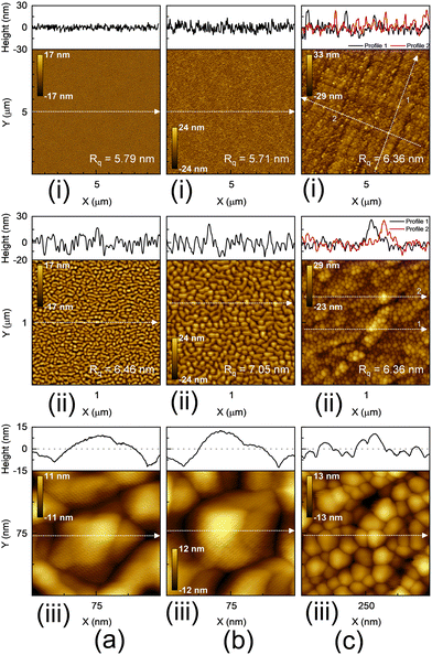 |
| | Fig. 2 AFM micrographs of 10 × 10 μm2, 2 × 2 μm2, and 0.15 × 0.15 μm2 (0.5 × 0.5 μm2) areas of sample: (a) Sample S1, (b) Sample S2, and (c) Sample S3, respectively. A line scan of Ge QDs corresponding to the dotted white line reveals a range of heights from ∼15 to 25 nm. | |
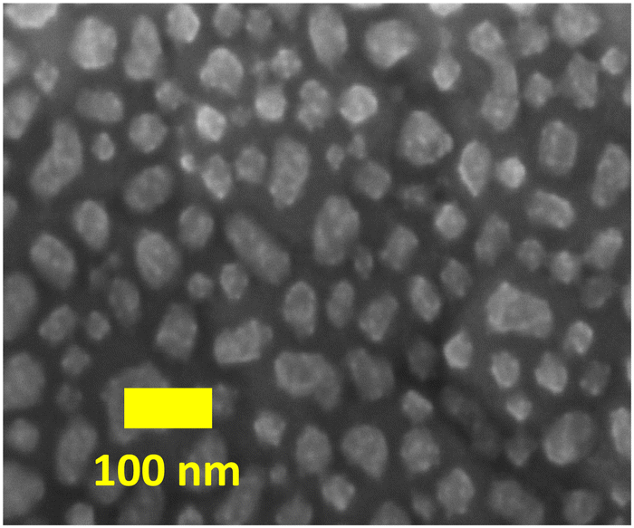
To further investigate the surface morphology and to confirm the AFM analysis results above, Sample S3 was studied by SEM secondary electron imaging since the AFM micrograph does not determine whether the QDs coalesce with each other and form a 2D along with 3D growth of Ge. Fig. 3 shows the sample surface looking directly down along the surface normal. The Ge dots are observed to be uncoalesced and possess a range of diameters of ∼20–80 nm with an average of ∼50 nm. The density of the dots is ∼320 μm−2. The observed long-range uniformity of the Ge QD distribution suggests that they do not exhibit any preference for nucleation sites. This result is consistent with the AFM result shown in Fig. 2(c.ii), where the dots uniformly follow the curvature of the crosshatch ridges. However, from Fig. 3, it is not clear if a 2D Ge wetting layer (Frank–van der Merwe) formed before the Ge growth transitioned to an island growth mode (Stanski–Krastanov). The strong contrast between the dots and flat regions suggests that the two regions may be composed of different materials, indicating the absence of a 2D Ge wetting layer. However, this is not conclusive since, in secondary electron imaging, the topographical contrast mechanism dominates the Z-contrast mechanism (where Z refers to the atomic number). While AFM and SEM analyses are unable to clarify the presence of a wetting layer, cross-sectional TEM images discussed below reveal that no wetting layer is present and that the growth is indeed fully 3D.
 |
| | Fig. 3 Top-down SEM secondary electron micrographs showing the surface morphology of Sample S3. | |
The formation of islands is driven by the misfit-induced strain at the Ge/In0.51Al0.49As or Ge/In0.53Ga0.47As heterointerface. Tersoff and LeGoues showed that the energy barrier to the formation of islands (or surface roughening) scales with ε−4, where ε is the in-plane misfit strain.34 While island formation increases the surface area, it allows for a net decrease of the total energy by permitting partial relaxation of the misfit-induced strain by purely elastic deformation on the growth surface. This relaxation mechanism was shown to compete with relaxation by dislocation formation, which was shown to have a much weaker dependence on ε.35 The difference in the dependencies on the misfit for the two mechanisms has dramatic implications for surface morphology and relaxation mechanics. In high-misfit systems ε > ε0, the energy barrier for roughening is lower than that for dislocation introduction; thus, the roughening mechanism dominates. For low-misfit systems ε < ε0, the reverse is true: (i) it is energetically preferable to relax by dislocation introduction, (ii) the initial dislocations diminish the driving force for roughening, and (iii) the resulting growth is 2D. This explains why, for high-misfit systems, QDs can form before any dislocations are introduced, resulting in pseudomorphic strained dots. The crossover points between the two regimes (i.e., the critical misfit ε0) can be determined experimentally for a given set of growth parameters (temperature, growth rate, surfactant, and grading rate) and material system. Current research work shows that for the Ge/InxAl1−xAs system, the critical misfit is exceeded since the In composition is 51%. This is the first study, to the author's knowledge, which presents experimental evidence of ε0 for this material system. Since the roughening argument presented by Tersoff and LeGoues34 did not assume a sign for the misfit, that is, whether the misfit is tensile or compressive, the nature of the competition between the relaxation by roughening and relaxation by dislocation formation is not expected to change substantially.
B Vibrational properties via Raman spectroscopy
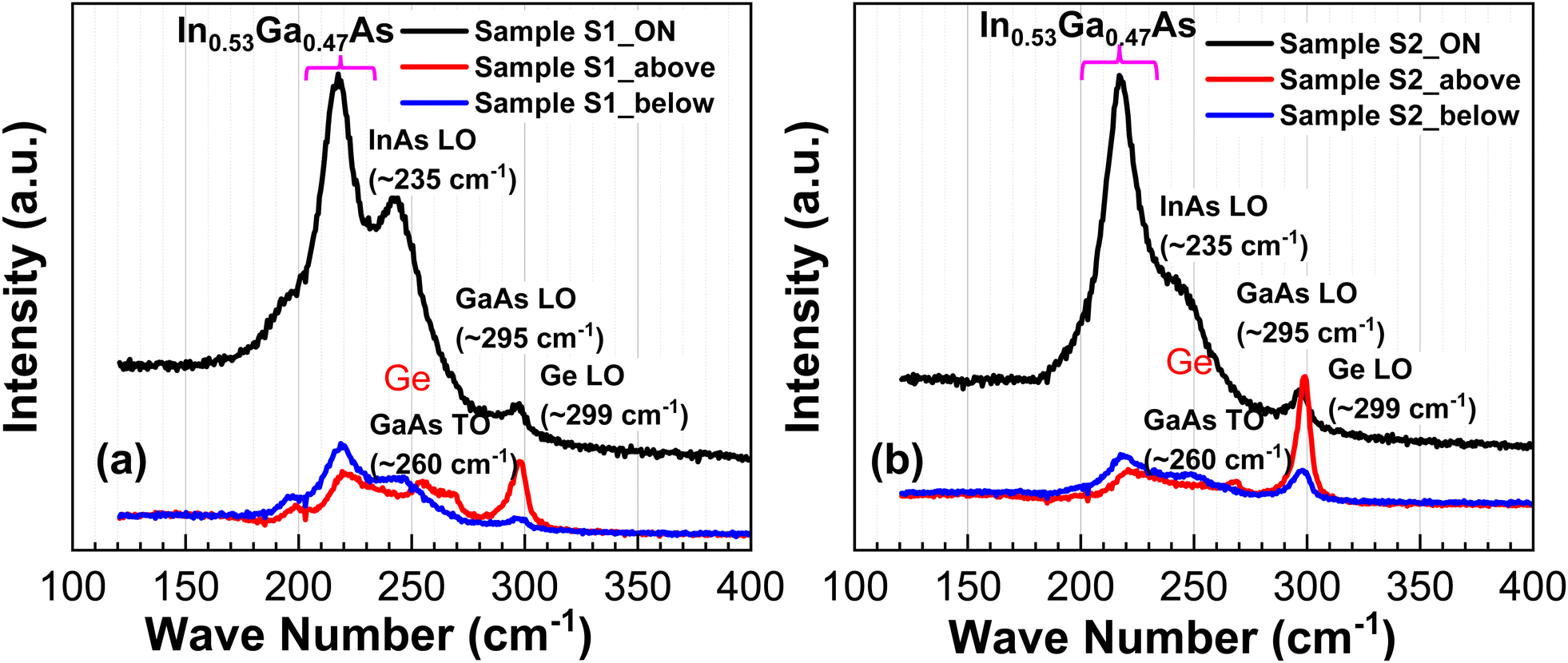
Raman spectroscopy analysis in backscattered geometry was used to determine the strain state in the Ge QDs of Samples S1 and S2 since this technique is widely used in semiconductor industries. Here, the Raman spectra of a Ge QD are similar to those of the thin-film semiconductor heterostructures. To record the information only from the Ge QD, one needs to focus the laser beam so that the intensity of the Raman spectra is the highest only from the Ge QD. This allows us to determine the longitudinal optical (LO) phonon peak of the Ge QDs. At its minimum spot size, the laser beam (while using the 100 × objective lens) is calibrated to obtain a ∼10 μm spot size. However, for the thin Ge QD (Sample S1) on InGaAs, this spot size is much larger than the size of a single Ge QD. The penetration depth of the 514.53 nm laser in Ge is approximately 19.2 nm. In such a scenario, the incident laser beam penetrates the InGaAs layer because the Ge QDs do not coalesce together, as shown in Fig. 3. Here, Raman spectra were collected from Samples S1 and S2, as shown in Fig. 4, where the Raman spectra were obtained from each layer structure under three different measurement conditions, where the laser was focused: above the Ge QDs, ON the QDs and below the QDs. One can find that the Raman signal intensity from the InGaAs layer is dominant in “ON” and “below” cases due to the lower volume of Ge QDs involved in the Raman signal. This is clear from the GaAs (LO, TO) and InAs (LO) phononic peaks in the mixed signal, whereas the peak from the Ge QD provides the true strain calculation. During these measurements, Raman spectra were also recorded from the bulk (100)Ge substrate, and the LO phonon peak was measured at ωo ∼ 300.5 cm−1. Any LO phonon peak shift with respect to ωo is considered a strain-induced peak shift. The tensile strain represents the shift in the peak towards the left and the compressive strain towards the right. Each measurement was performed at three locations in each layer structure. After analyzing the peak separation of each sample, we found that Samples S1 and S2 exhibit tensile strains of 0.38%–0.65% and 0.25%–0.38%, respectively, indicating that Ge QDs are typically relaxed with no retention of the calculated lattice misfit of ∼3.4% between the Ge and the underlying buffer layer. Note that a large number of Ge QDs provided a Raman signal since the area of the laser spot size was ∼78 μm2 (ON case). The relaxation properties of Ge QDs can be corroborated by X-ray and cross-sectional TEM analysis, as discussed below.
 |
| | Fig. 4 Raman signal from (a) Sample S1 and (b) Sample S2. | |
C Structural and compositional analysis via X-ray diffraction
The structural quality and relaxation state of the Ge QD structures were evaluated by high-resolution X-ray diffraction measurements. Fig. 5 shows the X-ray rocking curves obtained from the (004) Bragg lines of the Ge QDs grown on the InP and GaAs substrates of Samples S1, S2, and S3. The angular separation between the diffraction peaks of InP and InGaAs results from the difference in the lattice plane spacing, and the InGaAs layer is closely lattice-matched with the InP substrate for Samples S1 and S2. The peak separation between the InP substrate and InGaAs layer is <0.1°, and it is considered to be a closely lattice-matched InGaAs/InP system. For Sample S2, a broad reciprocal lattice point (RLP) of the Ge layer was observed at the peak position of ∼33° (same as the GaAs substrate RLP), indicating fully relaxed Ge QDs. Here, many Ge QDs provided the X-ray signal from Sample S2. On the other hand, there is no signal from the Ge QDs of Sample S1 due to the thinner volume of Ge materials for exhibiting the signal. Furthermore, for the linearly graded Al0.49In0.51x(Ga0.51)1−xAs buffer, the X-ray rocking curve confirms the gradual change in the lattice constant from the GaAs buffer (Sample 3) to the uppermost composition of In0.51Al0.49As. The location of the In0.51Al0.49As RLP near the In0.53Ga0.47As RLP confirms the fully relaxed metamorphic In0.51Al0.49As/Al0.49In0.51x(Ga0.51)1−xAs buffer. The relaxed Ge RLP was located at the same position as the GaAs substrate RLP. The presence of tensile strain inside the Ge QDs with enough volume36 could provide a signal other than that of the relaxed Ge RLP. Dey et al.36 studied the SEM and X-ray images of a QD with lateral dimensions of 150 nm × 110 nm, which implies that the QDs can only provide X-ray signals with larger dimensions. The reciprocal space maps would provide the relaxation state of each Ge QD structure, as discussed below. Symmetric (004) and asymmetric (115) RSMs were recorded from layer structures S2 and S3, and only (004) scans were recorded from Sample S1. The symmetric (004) RSMs from Samples S1, S2, and S3 are shown in Fig. 6 (asymmetric scans are not shown here). These RSMs were used to determine the In composition x of the InxAl1−xAs (InxGa1−xAs) layer, serving as the tensile-mismatched growth template for Ge. The presence of a small lattice tilt in the InAlAs layer (Fig. 6c) complicates the extraction of the in-plane lattice parameter a‖ from the (115) scan. The In0.51Al0.49As layer peak does not lie on the same vertical line as the substrate peak in the (004) RSM, which is direct evidence of the lattice tilt. Since the focus of this work is not a detailed compositional analysis, no attempt has been made to correct the tilt, and the assumption of 100% relaxation (a = ar) in the InAlAs layer has been utilized for compositional analysis. This assumption is reasonable since a high degree of relaxation is indicated by the presence of a 2D crosshatch pattern surface morphology, as seen in Fig. 2(c.i), which is further supported by the cross-sectional TEM analysis below. Due to the relatively small volume of Ge in the sample, the scattered X-ray intensity from the QDs coincided with the relaxed Ge RLP (Fig. 6c), which indicates that the Ge QDs were relaxed, supported by the Raman measurements where minute amounts of tensile strain were determined from Ge QDs. In addition, there was no RSM signal from Sample S1 since it was limited to a Ge layer thickness of 7 nm, which formed QDs due to the strain field. The PL measurements determine whether a thin layer of Ge exists within Sample S1. These results are discussed in the following sections.
 |
| | Fig. 5 Symmetric (004) X-ray rocking curves obtained from the 3 Ge QD layer structure studied in this work. The peak positions of each layer are identified and listed in this figure. | |
 |
| | Fig. 6 Symmetric (004) RSMs of Samples S1, S2, and S3. Reciprocal lattice point (RLP) of (a) InP substrate and In0.53Ga0.47As layer. Here, the signal from the Ge QD is not visible. (b) InP/InGaAs along with relaxed Ge QD RLP, (c) GaAs substrate, graded Al0.49In0.51x(Ga0.51)1−xAs buffer, and In0.51Al0.49As RLP. The relaxed Ge QD RLP coincided with the GaAs substrate RLP since both materials have almost the same lattice constant. | |
D Optical properties via PL spectroscopy
The optical properties of Samples S1 and S2 were evaluated by photoluminescence spectroscopy at room temperature since this method is widely used to qualify semiconductor materials via different optical transitions. Fig. 7(a) and (b) show the PL spectra collected from Samples S1 and S2, respectively. Curve fitting to each PL data was carried out to isolate the peak position. A single optical transition, with peak positions at 0.6716 eV and 0.7598 eV, was observed for Samples S1 and Sample S2, respectively. The emission peak from Sample S1 is attributed to carrier recombination from the Ge L-valley to the heavy/light hole, i.e., an indirect transition. In contrast, the optical transition from Sample S2 is ascribed as Ge Γ-valley to the heavy/light hole recombination, i.e., a direct transition. The laser power required to achieve the optical transition from Sample S2 is much higher than that from Sample S1 (350 mW versus 150 mW) and no signal was detected at 150 mW from Sample S2. This indicates that Ge QDs with larger heights relax the strain field and create more SFs than thinner Ge QD samples. A higher laser power generates more carriers, which are transferred to the Γ-valley. In contrast, low-power carriers are mostly confined within the L-valley due to the higher density of states. Based on these optical transitions, we infer that Ge QDs are relaxed. If these QDs were not relaxed, the peak position would have a longer wavelength due to the reduction of the Ge bandgap.
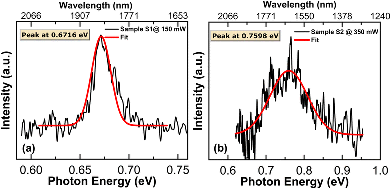 |
| | Fig. 7 PL signals from (a) Ge/In0.53Ga0.47As/InP (Sample S1) and (b) Ge/In0.53Ga0.47As/InP (Sample S2) structures. | |
E Heterointerface analysis via TEM
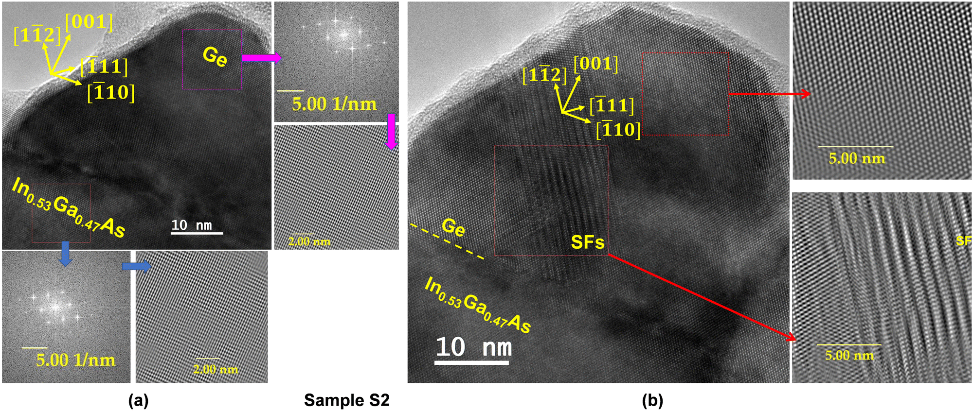
Fig. 8(a) and (b) show cross-sectional TEM micrographs of the full layer structure for Samples S2 and S3, respectively. The lattice mismatch-induced defects and dislocations are confined within the graded quaternary Al0.49In0.51x(Ga0.51)1−xAs buffer on the GaAs substrate, and the In0.53Ga0.47As layer is lattice-matched to the InP substrate. The constant-composition In0.51Al0.49As and In0.53Ga0.47As layers served as strain templates for the Ge layer. In both samples, a high degree of strain-induced ful 3D Ge growth was observed.34 The average island heights on the InGaAs and InAlAs virtual substrates are ∼40 nm and 20 nm, respectively. The difference in the island size is due to the slightly longer duration of Ge layer growth of the InGaAs sample, as discussed in the Experimental section. The InAlAs sample contained only uncoalesced islands, while the InGaAs sample contained a mixture of coalesced and uncoalesced islands, as shown in Fig. 8(a). Since dislocation-free Ge islands with greater heights have been observed for compressive growth on higher-mismatch Si substrates,37 it seems plausible that the Ge islands in both samples in this work might contain considerable tensile strain due to lower lattice misfit. Due to the small volume of Ge in these samples, X-ray diffraction methods for evaluating the precise strain could not be applied. By determining the RLP position of the relaxed Ge, we can infer that Ge QDs are relaxed in Sample S2. However, Raman measurements show only a minute amount (0.25%–0.38%) of tensile strain present within the Ge layer (Sample S2). Cross-sectional HR-TEM micrographs of representative Ge QDs from Samples S2 and S3 are shown in Fig. 9(a) and (b), respectively. The specimen foil was tilted such that the incident beam direction was aligned to the [![[1 with combining macron]](https://www.rsc.org/images/entities/char_0031_0304.gif) 0] crystallographic direction. The stacking faults of particular interest are marked by yellow dotted lines, and these SFs are associated with twin boundaries, as shown in Fig. 9(b). In addition, the two micro-twins annihilated each other, as shown in the inset of Fig. 9(b). Further investigation of Ge QDs grown on InGaAs VS reveals defect-free regions of the InGaAs buffer and Ge QDs, as shown in Fig. 10(a). Furthermore, a Ge QD showing the defect-free region and clusters of SFs (obtained by inverse-Fourier filtered micrographs) relieved the strain from Ge QD. One can see that certain parts of the Ge QD exhibit defect-free regions, but the net QD is relaxed by generating clusters of SFs, similar to those reported in ref. 25. The same types of defects were observed in the Ge QDs of both samples.
0] crystallographic direction. The stacking faults of particular interest are marked by yellow dotted lines, and these SFs are associated with twin boundaries, as shown in Fig. 9(b). In addition, the two micro-twins annihilated each other, as shown in the inset of Fig. 9(b). Further investigation of Ge QDs grown on InGaAs VS reveals defect-free regions of the InGaAs buffer and Ge QDs, as shown in Fig. 10(a). Furthermore, a Ge QD showing the defect-free region and clusters of SFs (obtained by inverse-Fourier filtered micrographs) relieved the strain from Ge QD. One can see that certain parts of the Ge QD exhibit defect-free regions, but the net QD is relaxed by generating clusters of SFs, similar to those reported in ref. 25. The same types of defects were observed in the Ge QDs of both samples.
 |
| | Fig. 8 Bright field cross-sectional TEM micrographs of (a) Ge/In0.53Ga0.47As/InP (Sample S2) and (b) Ge/In0.51Al0.49As/Al0.49In0.51x(Ga0.51)1−xAs/GaAs (Sample S3) layer structures examined in this work. | |
 |
| | Fig. 9 Cross-sectional TEM micrographs of representative Ge QDs from Samples S2 and S3. (a) Two Ge QDs are separated, and (b) SFs (marked by the yellow dotted line) are observed in each QD. The inset shows two micro-twins from one Ge QD that annihilated the other. | |
 |
| | Fig. 10 Cross-sectional TEM micrograph of representative Ge QD from Sample S2. (a) Ge QD along with two regions marked by two boxes: fast Fourier transform (FFT) in the Ge QD and the underlying In0.53Ga0.47As layer along with an inverse FFT of the same. (b) Ge QD showing the defect-free region and clusters of SFs (by inverse-Fourier filtered micrographs), relieving the strain from Ge QD. | |
As discussed above, the Ge QDs contain a negligible amount of tensile strain, and a high degree of relaxation is supported by the presence of both SFs and classic 60° misfit dislocations at the Ge/VS interfaces, as shown by HR-TEM. The relaxed islands grown on a highly tensile-mismatched (001) VS here contrast sharply with previous results of larger islands grown dislocation-free on a more highly compressive-mismatched Si(001) substrate.37 These divergent results demonstrate a central difference between the relaxation mechanics of the compressive-high misfit regime and the tensile-high misfit regime. The relaxation by Shockley partial dislocations (SPDs) in addition to perfect 60° dislocations in the tensile case (i) directly results in much higher SF densities and (ii) can facilitate faster relaxation since the Burger vector of the SPDs is smaller and is completely aligned with the resolved shear stress on the {111} planes.38 These effects are further supported by experimental reports based on GaP/Ga0.3As0.7P/GaP(001) double heterostructures,39 and comparisons of SixGe1−x alloys grown on tensile-mismatched Ge(001) or compressive-mismatched Si(001).40 It is well established that relaxation by surface roughening competes with relaxation by dislocation introduction in strained-layer epitaxy.34 One conclusion that this work, along with ref. 37–41, supports that in tensile (001) layer epitaxy there is additional competition: relaxation by perfect 60° dislocations competing with relaxation by SPDs with SFs.
The formation of the SFs themselves is explained by a mechanism proposed by Marée et al. and is based on the disassociation of the classic 60° dislocations into a pair of SPDs.38Fig. 11 shows a diagram of the SF formation mechanism using the hard-packed sphere model. The directions shown correspond to the case where the misfit is tensile, and the growth direction is (001). b0 represents the Burger vector of the classic 60° dislocations and is a full lattice translation vector (i.e., a perfect dislocation). In response to the resolved shear stress τ due to the mismatch, each sphere in the top plane shears from one A site to an adjacent A site, restoring the correct ABCABC stacking order but leaving a misfit dislocation at the interface. It is believed that in executing the b0 translation, the shearing plane does not move directly over the top of the B spheres (a high-energy path), but instead follows the lower energy path between the B spheres. This path corresponds to making the translation b1 and then b2 successively, where b1 and b2 are Burger vectors for a Shockley partial dislocation pair and is equivalent to the Burger vector reaction given by
where all three vectors lie on the same {111} slip plane. However, if only translation
b1 can be made and not
b2, the top plane now occupies C sites (believed to be local energy minima), and the stacking order is disrupted. The stacking order is now ABCBCABC – an A plane is missing – and an intrinsic SF has been introduced. This situation is illustrated in
Fig. 10(b). The angle between the resolved shear stress
τ and vectors
b1 and
b2, and the order in which the partial dislocations
b1 and
b2 must nucleate, play important roles in determining when this situation is likely to occur. In the case where the strain is tensile, and the growth direction is (001), as shown in
Fig. 11, the angles between
τ and
b1 and
b2 are 0° and 60°, respectively, corresponding to a factor of two differences in the shear force exerted on the 90° partial dislocation compared to that for the 30° partial dislocation. When the strain is compressive, the vectors
b0,
b1,
b2, and
τ are inverted, as shown in
Fig. 11.
38 Now the 30° partial, which is poorly aligned with
τ, must lead to the reaction sequence, as shown in the above equation. Once the 30° partial nucleates, the 90° partial follows immediately since
τ acts on 90° more efficiently, resulting in the annihilation of the SFs and the formation of a classic 60° perfect dislocation. It is important to note that since the resolved shear stress acts on the 30° partial inefficiently and since the 30° partial must nucleate before the 90° partial, the energy barrier for nucleating a dislocation can be higher in the compressive case than in the tensile case. In the tensile case, the 90° partial leads the reaction sequence, leaving open the possibility that the resolved shear stress may be sufficient to nucleate the 90° partial but not the 30° partial, which would result in SF. This may help explain why Eaglesham and Cerullo observed dislocation-free compressive Ge/Si(001) islands up to 50 nm in height,
37 and why a similar result was not observed in this work for the tensile case. Marée
et al. used this mechanism to explain a difference in the number of SFs experimentally observed between the tensile Si/GaP(001) interface and the compressive In
0.07Ga
0.93As/GaAs(001) interface,
38 but until now, there have been no reports of this occurring in tensile Ge/III–V interfaces. However, Wang
et al.25 demonstrated Ge QDs using selective oxidation of poly-Si
1−xGe
x lithographically patterned structures over Si
3N
4 layers, where 60 nm and 90 nm Ge QDs were relaxed. In addition, Chen
et al.42 demonstrated Ge QDs on InAlAs and InGaAs, where extensive defects were observed at the Ge/InGaAs heterointerface. This work confirms the instability of the tensile Ge/III–V heterointerface against the formation of SFs, which is a potential concern since SFs can be extremely detrimental to device performance in highly tensile-strained systems. However, the exact boundary of lattice misfit, where the tensile strain inhibits the formation of SFs, is not known. This work showed that the maximum biaxial tensile strain in Ge cannot be as high as 3.4% without the formation of SFs.
 |
| | Fig. 11 A hard-packed sphere model of the (11)planes showing how the perfect 60° dislocations with Burger vector b0 comprise two Shockley partial dislocations with Burger vectors b1 and b2. If the two partials do not nucleate and glide together as a pair, an SF forms along the planar length of the crystal between them. τ represents the resolved shear stress due to the tensile misfit strain on the (11) planes. The top-down direction in the diagram is [11]. The direction of the dislocation line in all cases is [0]. The dislocations are named based on the angle their Burger vector makes with the dislocation line. | |
If the growth direction is (011) or (111) instead of (001), the vectors in Fig. 11 are again inverted.43 The result is that the 30° partial must nucleate first in the tensile case and the 90° must nucleate first in the compressive case, rendering compressive films now unstable to SF formation instead of tensile films. This is supported by experimental studies of SFs in compressive non-(001) films.44,45 In these reports, researchers found that the critical layer thickness was shifted lower in compressive-(011) films compared to compressive-(001) films. This is because, in compressive-(011) films, the Burgers vector of the 90° SPD is completely aligned with τ on the inclined {111} planes (as shown in Fig. 11) and is, therefore, more efficient at accommodating that stress. This fact does not change between the tensile-(001) and compressive-(011) interfaces. Therefore, for at least some misfit regimes, the critical layer thickness for the tensile-(001) interface should also be shifted lower (with respect to the compressive-(001) case). It is also worth noting that since this work is based on observations of uncoalesced islands, this mechanism for relaxation by Shockley partial dislocations with SFs is now shown to be independent of any dislocation interaction that takes place during the coalescence of growing islands. This is the first work, to the author's knowledge, to elucidate this mechanism on uncoalesced islands.
Conclusion
Highly tensile-strained Ge layers were grown on two different metamorphic buffers, In0.53Ga0.47As and In0.51Al0.49As, by solid source molecular beam epitaxy, and their relaxation mechanisms were investigated. Due to the large lattice misfit, the Ge layer formed quantum dots with an average diameter and height of ∼50 nm and ∼20 nm, respectively, and a density of ∼320 μm−2 uniformly distributed over the underlying buffer. The instability of the highly tensile Ge(001) epitaxial layers against stacking fault formation was experimentally demonstrated in III–V buffers. HR-TEM indicated that the Ge QDs retained minimal tensile strain, and most of the lattice misfit strain (f = 3.5%) was relaxed by creating SFs. The mechanism driving the formation of SFs is consistent with the model proposed by Marée et al. for the relaxation of (001) oriented tensile layers by the nucleation of Shockley partial dislocations. All Ge QDs contain SFs of the close-packed {111} planes nucleated by Shockley partial dislocations with Burger vectors b = ⅙〈112〉. The SFs arise from a higher net force on the leading 90° disassociated components of the classic 60° dislocations compared to the trailing 30° disassociated components. This difference in forces can result in the separation or disassociation of the Shockley partial dislocation pairs, inhibiting them from traveling together, i.e., 60° dislocations. In the low and intermediate tensile-misfit regimes (ε < 2.0), undisassociated 60° dislocations remain energetically favorable due to the additional energy required to form a stacking fault. The required stacking fault energy effectively acts as an additional force on each partial dislocation that holds the Shockley pair together. As a result, the low and immediate tensile-misfit regimes are much less affected by the instability phenomena, and the tensile strain needed to achieve a Ge direct bandgap is reported to be less than 2.0%,15,20 suggesting that a direct bandgap Ge can be achieved before triggering the SF formation instability. Hence, the maximum tensile strain that can be realized in Ge without the formation of Shockley partial dislocations is lower than 3%. Further investigations are necessary as a function of the tensile strain in Ge on a III–V virtual substrate or smaller quantum dots that can retain the strain without relaxation by creating stacking faults.
Author contributions
The manuscript was written through the contributions of all authors. All authors have approved the final version of the manuscript.
Data availability
This research paper contains purely experimental findings, and no external data or software was used to develop conclusions. However, if any measurement data is required, they can be made available upon request from the corresponding author.
Conflicts of interest
There are no conflicts to declare.
Acknowledgements
M. K. H. and S. K. acknowledge partial support from the NSF under grant number ECCS-2042079, a US–Ireland Joint R&D Program and Virginia Tech Nanoscale Characterization and Fabrication Laboratory and Virginia Tech Nanofabrication facilities for assistance during materials analysis. M. K. H. acknowledges the contribution of M. Clavel for assisting epitaxial growth and P. Goley for TEM/SEM measurements and technical discussions. In addition, the authors acknowledge the Virginia Tech College of Engineering for seed funding for quantum technology research. G. A. K. acknowledges the support of the Air Force Office of Scientific Research DURIP funding (FA9550-16-1-0358).
Notes and references
- Y. Zhu, D. Maurya, S. Priya and M. K. Hudait, ACS Appl. Electron. Mater., 2014, 6, 4947 CrossRef CAS PubMed.
- K.-H. Kao, A. S. Verhulst, M. Van de Put, W. G. Vandenberghe, B. Soree, W. Magnus and K. De Meyer, J. Appl. Phys., 2014, 115, 044505 CrossRef.
- S. Wirths, A. Tiedemann, Z. Ikonic, P. Harrison, B. Holländer, T. Stoica, G. Mussler, M. Myronov, J. Hartmann and D. Grützmacher, Appl. Phys. Lett., 2013, 102, 192103 CrossRef.
- J.-S. Liu, M. Clavel and M. K. Hudait, IEEE Trans. Electron Devices, 2015, 62, 3223 Search PubMed.
- M. Clavel, D. Saladukha, P. Goley, T. J. Ochalski, F. Murphy-Armando, R. J. Bodnar and M. K. Hudait, IEEE J. Electron Devices Soc., 2015, 3, 184 Search PubMed.
- J.-S. Liu, M. Clavel and M. K. Hudait, IEEE Trans. Electron Devices, 2017, 64, 2193 CAS.
- J.-S. Liu, M. Clavel and M. K. Hudait, IEEE J. Electron Devices Soc., 2019, 7, 210 CAS.
- J. Liu, X. Sun, D. Pan, X. Wang, L. C. Kimerling, T. L. Koch and J. Michel, Opt. Express, 2007, 15, 11272 CrossRef CAS PubMed.
- R. Soref, Nat. Photonics, 2010, 4, 495 CrossRef CAS.
- M. K. Hudait, F. Murphy-Armando, D. Saladukha, M. B. Clavel, P. S. Goley, D. Maurya, S. Bhattacharya and T. J. Ochalski, ACS Appl. Electron. Mater., 2021, 10, 4535–4547 CrossRef.
- M. K. Hudait, M. B. Clavel, S. Karthikeyan and R. Bodnar, ACS Appl. Electron. Mater., 2023, 5, 4792 CrossRef CAS.
- Y.-J. Yang, W. Ho, C.-F. Huang, S. Chang and C. Liu, Appl. Phys. Lett., 2007, 91, 102103 CrossRef.
- X. Sun, J. Liu, L. C. Kimerling and J. Michel, Opt. Lett., 2009, 34, 1198 CrossRef CAS PubMed.
- J. R. Jain, A. Hryciw, T. M. Baer, D. A. Miller, M. L. Brongersma and R. T. Howe, Nat. Photonics, 2012, 6, 398 CrossRef CAS.
- M. V. Fischetti and S. E. Laux, J. Appl. Phys., 1996, 80, 2234 CrossRef CAS.
- M. B. Clavel, F. Murphy-Armando, Y. Xie, K. T. Henry, M. Kuhn, R. J. Bodnar, G. A. Khodaparast, D. Smirnov, J. J. Heremans and M. K. Hudait, Phys. Rev. Appl., 2022, 18, 064083 CrossRef.
- D. Saladukha, M. B. Clavel, F. Murphy-Armando, G. Greene-Diniz, M. Gruening, M. K. Hudait and T. J. Ochalski, Phys. Rev. B, 2018, 97, 195304 CrossRef CAS.
-
M. K. Hudait, M. Clavel, L. Lester, D. Saladukha, T. Ochalski and F. Murphy-Armando, Proc. SPIE 9755, Quantum Sensing and Nano Electronics and Photonics XIII, 97550Y (February 13, 2016).
- M. Clavel, D. Saladukha, P. Goley, T. J. Ochalski, F. Murphy-Armando, R. J. Bodnar and M. K. Hudait, ACS Appl. Mater. Interfaces, 2015, 7, 26470 CrossRef CAS PubMed.
- R. A. Soref and L. Friedman, Superlattices Microstruct., 1993, 14, 189 CrossRef CAS.
- R. Jakomin, M. de Kersauson, M. El Kurdi, L. Largeau, O. Mauguin, G. Beaudoin, S. Sauvage, R. Ossikovski, G. Ndong, M. Chaigneau, I. Sagnes and P. Boucaud, Appl. Phys. Lett., 2011, 98, 091901 CrossRef.
- Y. J. Huo, H. Lin, R. Chen, M. Makarova, Y. W. Rong, M. Y. Li, T. I. Kamins, J. Vuckovic and J. S. Harris, Appl. Phys. Lett., 2011, 98, 011111 CrossRef.
- Y. Bai, K. E. Lee, C. Cheng, M. L. Lee and E. A. Fitzgerald, J. Appl. Phys., 2008, 104, 084518 CrossRef.
- E. Fitzgerald, Mater. Sci. Rep., 1991, 7, 87 CrossRef CAS.
-
I.-H. Wang, P.-Y. Hong, K.-P. Peng, H.-C. Lin, T. George and P.-W. Li, 2020 IEEE International Electron Devices Meeting (IEDM), 12–18 December 2020. pp. 841–844.
- M. K. Hudait, M. Clavel, P. Goley, N. Jain and Y. Zhu, Sci. Rep., 2014, 4, 6964 CrossRef CAS PubMed.
- L. A. Terrazos, E. Marcellina, Z. Wang, S. N. Coppersmith, M. Friesen, A. R. Hamilton, X. Hu, B. Koiller, A. L. Saraiva, D. Culcer and R. B. Capaz, Phys. Rev. B, 2021, 103, 12 CrossRef.
- A. Sammak, D. Sabbagh, N. W. Hendrickx, M. Lodari, B. P. Wuetz, A. Tosato, L. Yeoh, M. Bollani, M. Virgilio, M. A. Schubert, P. Zaumseil, G. Capellini, M. Veldhorst and G. Scappucci, Adv. Funct. Mater., 2019, 29, 1807613 CrossRef.
- S. Siontas, D. Li, H. Wang, A. V. P. S. Aravind, A. Zaslavsky and D. Pacifici, Mater. Sci. Semicond. Process., 2019, 92, 19–27 CrossRef CAS.
- C.-C. Lai, R. C. Pan, I.-H. Wang, T. George, H.-C. Lin and P.-W. Li, IEEE J. Electron Devices Soc., 2023, 11, 54 CAS.
- P. Y. Hong, C. C. Lai, T. Tsai, H.-C. Lin, T. George, P.-W. Li and D. M. T. Kuo, Sci. Rep., 2023, 13, 14333 CrossRef CAS PubMed.
- M. Haupt, K. Köhler, P. Ganser, S. Emminger, S. Müller and W. Rothemund, Appl. Phys. Lett., 1996, 69, 412 CrossRef CAS.
- M. K. Hudait, M. Meeker, J.-S. Liu, M. B. Clavel, S. Bhattacharya and G. A. Khodaparast, Opt. Mater., 2022, 131, 112633 CrossRef CAS.
- J. Tersoff and F. LeGoues, Phys. Rev. Lett., 1994, 72, 3570 CrossRef CAS PubMed.
- F. LeGoues, P. Mooney and J. Tersoff, Phys. Rev. Lett., 1993, 71, 396 CrossRef CAS PubMed.
- A. B. Dey, M. K. Sanyal, A. Schropp, S. Achilles, T. F. Keller, I. Farrer, D. A. Ritchie, F. Bertram, C. G. Schroer and O. H. Seeck, ACS Nano, 2023, 17, 16080 CrossRef CAS PubMed.
- D. Eaglesham and M. Cerullo, Phys. Rev. Lett., 1990, 64, 1943 CrossRef CAS PubMed.
- P. Maree, J. Barbour, J. Van der Veen, K. Kavanagh, C. Bulle-Lieuwma and M. Viegers, J. Appl. Phys., 1987, 62, 4413 CrossRef CAS.
- J. Petruzzello and M. Leys, Appl. Phys. Lett., 1988, 53, 2414 CrossRef.
- W. Wegscheider and H. Cerva, J. Vac. Sci. Technol., B, 1993, 11, 1056 CrossRef CAS.
-
C. Claeys and E. Simoen, Extended defects in germanium: fundamental and technological aspects, Springer, 2008, vol. 118 Search PubMed.
- Q. Chen, L. Zhang, Y. Song, X. Chen, S. Koelling, Z. Zhang, Y. Li, P. M. Koenraad, J. Shao, C. S. Tan, S. Wang and Q. Gong, ACS Appl. Nano Mater., 2021, 4, 897 CrossRef CAS.
- E. Kvam and R. Hull, J. Appl. Phys., 1993, 73, 7407 CrossRef CAS.
- R. Hull, J. Bean, L. Peticolas and D. Bahnck, Appl. Phys. Lett., 1991, 59, 964 CrossRef CAS.
- R. Hull, J. Bean, L. Peticolas, D. Bahnck, B. Weir and L. Feldman, Appl. Phys. Lett., 1992, 61, 2802 CrossRef CAS.
|
| This journal is © The Royal Society of Chemistry 2024 |
Click here to see how this site uses Cookies. View our privacy policy here. 
 Open Access Article
 This Open Access Article is licensed under a Creative Commons Attribution-Non Commercial 3.0 Unported Licence
 *a,
S.
Bhattacharya
*a,
S.
Bhattacharya