
Spray-assisted deposition of a SnO2 electron transport bilayer for efficient inkjet-printed perovskite solar cells†
Vinayak Vitthal
Satale
 a,
Neetesh
Kumar
a,
Hock Beng
Lee
a,
Manoj Mayaji
Ovhal
a,
Sagnik
Chowdhury
a,
Barkha
Tyagi
a,
Asmaa
Mohamed
ab and
Jae-Wook
Kang
*a
a,
Neetesh
Kumar
a,
Hock Beng
Lee
a,
Manoj Mayaji
Ovhal
a,
Sagnik
Chowdhury
a,
Barkha
Tyagi
a,
Asmaa
Mohamed
ab and
Jae-Wook
Kang
*a
aDepartment of Flexible and Printable Electronics, LANL-CBNU Engineering Institute-Korea, Jeonbuk National University, Jeonju 54896, Republic of Korea. E-mail: jwkang@jbnu.ac.kr
bDepartment of Physics, Faculty of Science, South Valley University, Qena 83523, Egypt
First published on 10th May 2023
Abstract
Developing an efficient electron transport layer (ETL) through structural modification is essential to produce high-performance perovskite solar cell (PSC) devices. Specifically, the ETL should exhibit low defects, high optical transparency, and charge selectivity for ideal electron transport. Herein, we demonstrate (i) the low-temperature fabrication of tin oxide (SnO2) ETLs with a bilayer structure, and (ii) inkjet-printing of triple-cation perovskite films. Through the combined use of spin-coating and spray deposition, the optimized SnO2-bilayer ETL shows a nano-granule-textured surface, noticeably fewer defects, and a cascade conduction band position with the inkjet-printed perovskite film. The champion PSC device, based on the SnO2-bilayer ETL and inkjet-printed perovskite film, recorded an outstanding power conversion efficiency (PCE) of ∼16.9%, which is significantly higher than the device based on the conventional SnO2 ETL (PCE ∼14.8%). The improved photovoltaic performance of the SnO2-bilayer-based device arises mainly from more efficient charge transport and suppressed recombination at the ETL/perovskite interface. The SnO2-bilayer ETL and inkjet-printed perovskite films demonstrated herein can be potentially used for large-scale manufacturing of photovoltaic modules.
1. Introduction
In recent years, the power conversion efficiency (PCE) of lab-scale perovskite solar cells (PSCs) has reached an astoundingly high value of 25.7% by virtue of structural and defect engineering.1 Conventionally, the perovskite photoabsorber films in PSCs are deposited using one-step antisolvent or two-step sequential deposition methods, both of which rely heavily on the spin-coating process.2,3 The well-known spin-coating technique relies on centrifugal forces to generate the necessary liquid–vapor interface for perovskite film deposition, and thus, it exhibits poor scalability and limits the commercialization potential of PSCs. Consequently, numerous deposition methods that offer low raw material utilization rates and high film uniformity, such as vacuum deposition,4 spray deposition,5 brush painting,6 doctor-blade coating,37 and inkjet printing,7 have been explored for the large-scale preparation of perovskite films. Among these methods, inkjet printing (IJP) is the most material-efficient technique because it offers high cost-effectiveness, high writing accuracy, and a near-unity material utilization ratio.8,9 The IJP technique has been popular for fabricating large-area perovskite films with a precisely-controlled thickness and interface, yielding satisfactory performance in planar PSCs.10 Currently, the highest PCE achieved by inkjet-printed perovskite solar cell (IJP-PSC) is 21.7%, based on the p-i-n type configuration.11 The IJP technique also allowed the fabrication of PSC devices with all-inkjet-printed perovskite absorbers and charge extraction layers with a maximum PCE of 17.2%.7 Li et al. successfully prepared a large-area PSC device using the IJP technique and achieved a PCE of 18.64%.12 The overall performance of IJP-PSCs is converging upon the state-of-the-art values achieved by solution-processed PSCs.In the initial phase of the investigation, TiO2 as an electron transport layer (ETL) was commonly used in n-i-p structured PSCs owing to its outstanding electronic and optical properties.13,14 Based on the use of the mesoscopic TiO2 ETL and inkjet-printed MAPbI3 perovskite, the PSC achieved a maximum PCE of 12.3%.15 However, the high processing temperature (>450 °C), low conductivity, and vulnerability to photo-oxidation of the TiO2 layer make it less desirable for long-term use in PSCs.13 As a replacement for TiO2, low-temperature processable (<185 °C) ETLs such as ZnO,16 WO3,17 NbOx,18 CeOx,38 Fe2O3,19 and SiO2![[thin space (1/6-em)]](https://www.rsc.org/images/entities/char_2009.gif) 20–22 were introduced and applied in PSCs. In particular, SnO2 has been investigated extensively due to its highly comparable optoelectronic properties with TiO2, including high optical transparency and charge selectivity, excellent electron mobility (240 cm2 V−1 s−1), and more importantly, low-temperature processability.23 Furthermore, SnO2 has a favorable energy level alignment with the commonly used FAPbI3/MAPbI3 perovskites, i.e. having conduction and valence band edges below the perovskite absorber for efficient charge collection and blocking at the ETL/perovskite interfaces.23
20–22 were introduced and applied in PSCs. In particular, SnO2 has been investigated extensively due to its highly comparable optoelectronic properties with TiO2, including high optical transparency and charge selectivity, excellent electron mobility (240 cm2 V−1 s−1), and more importantly, low-temperature processability.23 Furthermore, SnO2 has a favorable energy level alignment with the commonly used FAPbI3/MAPbI3 perovskites, i.e. having conduction and valence band edges below the perovskite absorber for efficient charge collection and blocking at the ETL/perovskite interfaces.23
In its pristine state, solution-processed SnO2 exhibits a defect-rich nature, which is undesirable for its role as the ETL. To reduce the defect states and enhance the energy band structure, SnO2 has been used in tandem with other metal oxides, such as TiO2, to form a bilayer ETL for solution-processed PSC devices, resulting in improved charge extraction and a PCE of ∼19.8%.24 Thereafter, an amorphous-crystalline SnO2-bilayer with a unique morphology was developed using a low-temperature solution process, further boosting the PCE of PSCs to 20.39% by virtue of improved charge transfer at the SnO2/perovskite interface.25 These works have demonstrated the advantages of low-temperature processed bilayer ETLs which leads to the enhanced performance of solution-processed PSCs. In the current stage, the use of the SnO2 ETL is less popular for IJP-PSCs. Initially, a mesoporous TiO2 ETL and FAMAPbBr3 absorber were used to fabricate PSC devices, which showed a good PCE of 14.11%.26 Also, MAPbI3 and CsFAMAPb(Br, I)3-based IJP-PSCs fabricated with TiO2 as the ETL have achieved maximum PCEs of 18.20% and 19.60%.12,27 The IJP-PSC devices fabricated with modified compact and mesoporous TiO2 ETLs exhibited a PCE of 9.1%.28 To the best of our knowledge, there is only one report demonstrating the use of an SnO2 ETL for IJP-PSCs, in which a PCE of 10.35% was achieved by incorporating polymer additives into the perovskites.29 To improve the charge transfer without altering the optical properties of ETLs, the utilization of bilayer ETLs can be a successful strategy for enhancing the device performance of IJP-PSCs.
Here, we rationally designed a highly crystalline SnO2-bilayer ETL via the combined use of spin-coating and spray-deposition approaches. Specifically, a ∼30 nm thick SnO2 underlayer was first deposited on the substrate by spin-coating the sol–gel precursor, followed by the spray deposition of SnO2 colloidal solution to produce an overlaying scaffold layer. In this individual case, the spin-coated SnO2 (spin-SnO2) film exhibits a smooth yet compact surface, whereas the spray-deposited SnO2 (spray-SnO2) film has a mesoporous, nanograin-textured surface. Therefore, the resulting SnO2-bilayer ETL can inherit the exceptional morphological features found in both spin-SnO2 and spray-SnO2 films. The characterization confirmed that the SnO2-bilayer exhibits better morphology, reduced defects, and more suitable conduction and valence band alignments with the inkjet-printed perovskite layer than the commonly used spin-SnO2. The results show that the SnO2-bilayer can prevent direct contact among the ITO/perovskite layers more effectively than the spin-SnO2 and spray-SnO2 ETLs. At the same time, the SnO2-bilayer also exhibited a nano-granule-textured surface which produces larger surface-to-volume ratios as compared with spin-SnO2 and spray-SnO2 single-layer films, creating a maximum ETL/absorber interfacial area for efficient charge transport. Thus, the best SnO2-bilayer-based IJP-PSC successfully attained a maximum PCE of 16.9%, and its significantly higher PCE is associated with the spin-SnO2 based devices. The spray-assisted SnO2-bilayer ETL developed herein can be potentially used to develop large-scale IJP-PSC devices with improved performance and durability.
2. Results and discussion
2.1 Structural, morphological, and optoelectronic properties of SnO2 films
The SnO2-bilayer ETL was fabricated using a two-step strategy, i.e. spin coating the sol–gel precursor solution and a spray deposition technique, as demonstrated in Fig. 1(a). The synthesis parameters for spray coating have been applied as mentioned in the previous literature21 to produce high-quality SnO2 films. In the digital photographs of the spin-SnO2, spray-SnO2, and SnO2-bilayer films shown in Fig. 1(b), the color of the SnO2-bilayer film is more greenish than the spin and spray-SnO2 films. Based on the water contact angle (WCA) profiles displayed in Fig. 1(c), the spray-SnO2 (θ ∼41°) and SnO2-bilayer (θ ∼46°) films showed more hydrophobic behavior than the spin-SnO2 (θ ∼25°) film. As discussed in previous work,30 the wettability of the substrate or ETL/HTL and the growth of perovskite grains are closely linked. Low-density nuclei are produced on the hydrophobic substrate in the initial nucleation step, and can further expand and coarsen to larger grains during the thermal annealing step. Fig. 1(d) displays the X-ray diffraction (XRD) patterns of the spin-SnO2, spray-SnO2, and SnO2-bilayer films, broad diffraction peaks with lower intensity owing to the ultra-fine size (∼3 nm) of SnO2.21 The diffraction peaks observed in all the three films at the 2θ values of 26.6°, 33.9°, 38.8°, 51.8°, and 65.91° corresponding to the (110), (101), (200), (211), and (310) planes, respectively. These spectra match well with JCPDS no.: 01-072-1147, confirming the tetragonal crystal structure of tin oxide.21 | ||
| Fig. 1 (a) Schematic illustration of the fabrication process of SnO2-bilayer films, (b) digital photographs of SnO2 films coated on patterned ITO substrates, (c) contact angles of water on spin-SnO2, spray-SnO2, and SnO2-bilayer films, (d) XRD patterns, and (e) transmittance spectra and the Tauc plot (inset) of spin-SnO2, spray-SnO2, and SnO2-bilayer films. | ||
The prepared spin-SnO2, spray-SnO2, and SnO2-bilayer films over glass substrates were used for further studies. The transmittance spectra of all three SnO2 films were recorded using a UV-visible spectrometer and are shown in Fig. 1(e). The transmittance values at a wavelength of 550 nm for spin-SnO2, spray-SnO2, and SnO2-bilayer films are 96.9%, 96.3%, and 95.6%, respectively, and this trend matches well with previous work.25 The thickness (obtained from the surface profilometer) of the spin-SnO2 is ≈30 nm, and that of spray-SnO2 is ≈60 nm,21,25 whereas the thickness of the SnO2-bilayer was quite increased with a value of ≈80 nm. The reduction in the transmittance can be associated with the increased thickness of bilayer-SnO2 films. The optical band gap (Eg) of the different SnO2 ETLs was calculated from the Tauc plot (inset) in Fig. 1(e). The obtained Eg values for spin-SnO2, spray-SnO2, and SnO2-bilayer films are ∼3.69 eV, ∼3.61 eV, and ∼3.59 eV, respectively. The small change in Eg is due to the substantial variation in the band alignment of the SnO2 resulting from surface texture upgradation.
The surface texture of the spin-SnO2, spray-SnO2, and SnO2-bilayer films was investigated using a field-emission scanning electron microscope (FE-SEM). From the FE-SEM images in Fig. 2(a), the spin-SnO2 film had a compact morphology, whereas the surfaces of spray-SnO2 and SnO2-bilayer films were covered with ultrafine granular structures. The average size of the nano-granules in the spray and SnO2-bilayer films was ∼40 nm. These granules on the spray and SnO2-bilayer film surfaces are also visible through atomic force microscopy (AFM) analysis. The micrographs shown in Fig. 2(b) reveal that these granules were absent on the surface of spin-SnO2, which confirms that it can be only formed during the in situ spray coating process.21 Their nano-textured-granule structure, spray-SnO2, and SnO2-bilayer films exhibited a slightly larger specific root-mean-square (RMS) roughness values of ∼2.7 nm and ∼2.6 nm compared with spin-SnO2 (RMS ≈2.1 nm). These ultrafine granules give rise to a mesoporous morphology in the spray-SnO2 and SnO2-bilayer films, which can increase the contact area at the interface of the ETL/absorber for efficient charge collection.21,25
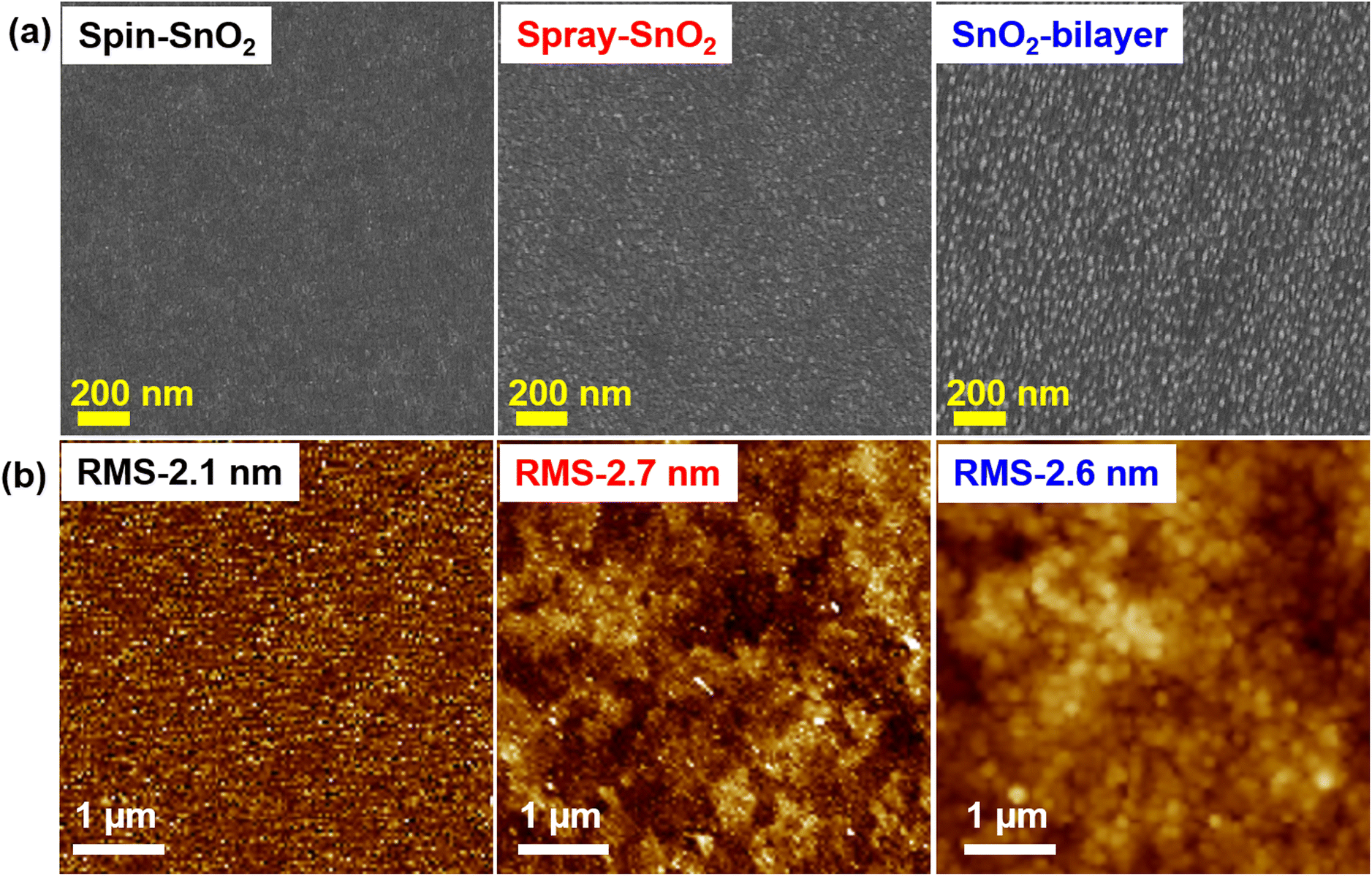 | ||
| Fig. 2 (a) Top-view FE-SEM images and (b) AFM micrographs depicting the surface morphologies and topographies of spin-SnO2, spray-SnO2, and SnO2-bilayer films. | ||
X-ray photoelectron microscopy (XPS) analysis was performed to study the surface elemental composition of the spin-SnO2, spray-SnO2, and SnO2-bilayer films. Fig. 3a describes that the O 1s core level spectra of three SnO2 films were elaborated into different oxygen components, namely O1, O2, and O3. Precisely, the major O1 peak situated at a lower binding energy (BE) of ≈530 eV is related to the lattice oxygen in the Sn–O, however, the minor O2 (≈531.5 eV) and O3 (≈532.5 eV) peaks are correlated with the oxygen vacancies (VO) and dangling hydroxyl (–OH) groups confined in SnO2, respectively.25,31
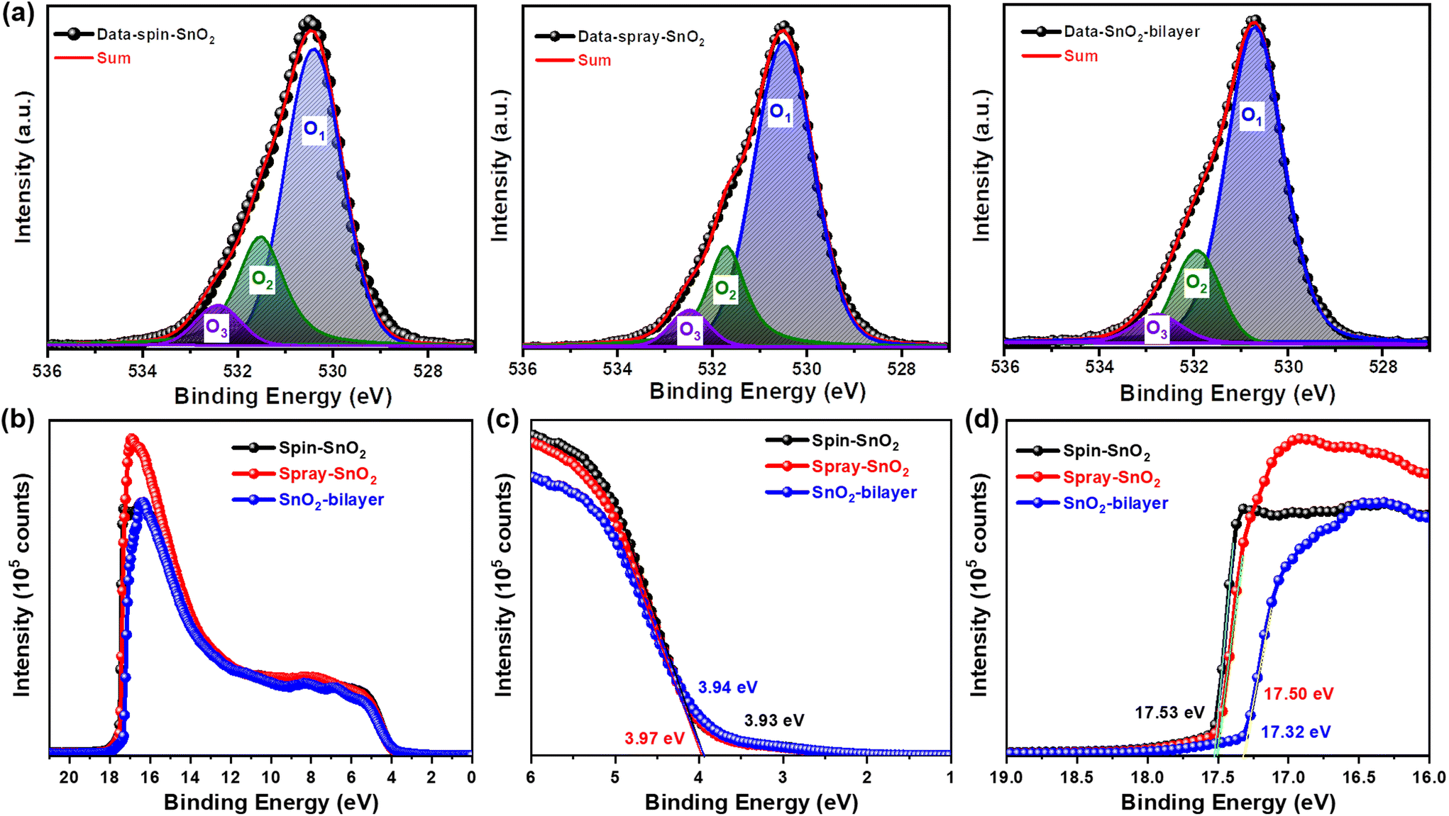 | ||
| Fig. 3 (a) XPS spectra of the O 1s core level of different SnO2 films (spin-SnO2, spray-SnO2, and SnO2-bilayer) on ITO glass. (b) Ultraviolet photoelectron spectroscopy (UPS) spectra, (c) on-set region, and (d) cut-off region of spin-SnO2, spray-SnO2, and SnO2-bilayer films. | ||
The amount of lattice (Olattice; O1) and defects (Odefect; O2 + O3) for oxygen atoms were estimated for all SnO2 films by calculating the area under the curve for every O component. In Table S1,† it is presented that the spin-SnO2 film exhibited a larger [Odefect/Olattice] fraction of ≈0.41, indicating the abundance of oxygen-related defects in the spin-SnO2 film surface acquired. In contrast, the SnO2-bilayer film exhibited the lowest fraction of [Odefect/Olattice] ≈0.28, suggesting that the presence of very few oxygen defects and the O component originates mainly from Sn–O. A lower fraction [Odefect/Olattice] of the SnO2-bilayer film initiates mostly from the decrease of –OH groups (O3). The main reason for the dominant charge transport from the ETL/absorber interface can be related to these –OH groups and VO defects which create recombination sites on the ETL surfaces. Hence, the knowingly fewer O-defects in the SnO2-bilayer film are incredibly advantageous for charge transport in PSCs.
Alongside the XPS measurements, UPS measurements were conducted to investigate the energy band alignments of all SnO2 films. Fig. 3(b–d) present the UPS spectra of the SnO2 films, cut-off edge, and valence band region. The values of Ecut-off and Eon-set were extracted from Fig. 3(c and d) for all SnO2 films and are summarized in Table S2.† Using Expression S1,† the work function (WS) values of the spin-SnO2, spray-SnO2, and SnO2-bilayer films were estimated to be −3.69, −3.72, and −3.90 eV, respectively. Meanwhile, the valence band energy levels (EVB) of the spin-SnO2, spray-SnO2, and SnO2-bilayer films were estimated as −7.62, −7.69, and −7.84 eV, individually (Expression S2†). The calculated conduction band energy level (ECB) values for the spin-SnO2 (−4.04 eV), spray-SnO2 (−3.97 eV), and SnO2-bilayer (−4.11 eV) films reveal the deeper ECB of the SnO2-bilayer could effectively transfer the electrons from the perovskite to SnO2. In addition, the deeper EVB of the spray-SnO2 and SnO2-bilayer than the spin-SnO2 possibly will efficiently reduce bimolecular recombination at the SnO2/absorber interface, which can improve the charge transport. The XPS and UPS outcomes taken together verify the alterations in the elemental composition and the exact energy band position of the SnO2-bilayer ETL can contribute positively to the performance of inkjet-printed photovoltaic devices.
2.2 Structural, morphological, and optoelectronic properties of inkjet-printed perovskite films
Fig. 4(a) schematically illustrates the inkjet-printing process of triple-cation perovskite films on different SnO2 ETLs. The structural information and crystal phase of the resulting inkjet-printed SnO2/perovskite films were analyzed using an X-ray diffractometer. Based on the XRD patterns in Fig. 4b, all of the perovskite films displayed a prominent peak corresponding to the (001) plane at a 2θ value of ∼14.1° regardless of the SnO2 underlayers. In addition to the (001) peak, other representative peaks such as (011), (111), (002), (012), (112), (022), and (003) were also detected, which can be indexed to the cubic crystal structure of the CsFAMAPbBrxI3−x perovskite.32,33 Comparatively, the intensities of the (001) and (002) planes in the SnO2-bilayer/perovskite film are relatively higher than those of the spin-SnO2/perovskite and spray-SnO2/perovskite samples, implying the superior crystallinity of the perovskite film in the former. A low-intensity subtle peak of the δ-phase34 perovskite was observed at 11.78° in all three samples, indicating the incomplete transformation of the δ-phase (yellow) perovskite to the α-phase (black) perovskite.32 The PbI2 peak was not detected in all of the samples, indicating the formation of highly crystalline perovskite films over different SnO2 underlayers. The estimated crystallite sizes (Debye–Scherrer formula) for the spin-SnO2/perovskite, spray-SnO2/perovskite, and SnO2-bilayer/perovskite samples were calculated to be ∼34.5 nm, 36.4 nm, and 36.5 nm, respectively. | ||
| Fig. 4 (a) Schematic illustration of perovskite film fabrication using inkjet printing. (b) X-ray diffraction (XRD) patterns of inkjet-printed perovskite films fabricated on spin-SnO2, spray-SnO2, and SnO2-bilayer ETLs. (c) UV-vis spectra and the Tauc plot (inset) of inkjet-printed perovskite films fabricated on spin, spray, and SnO2-bilayer ETLs. (d) Steady-state photoluminescence (PL) spectra of inkjet-printed perovskite films fabricated on spin, spray, and SnO2-bilayer ETLs. | ||
Furthermore, all of the SnO2/inkjet-printed perovskite films revealed an absorption edge in the region of 760–770 nm (Fig. 4c), and estimated values of Eg ≈1.63–1.61 eV (inset). Simultaneously, steady-state photoluminescence (PL) results revealed the electron extraction dynamics at the SnO2/perovskite interface, and the resulting PL spectra are displayed in Fig. 4(d). The reference inkjet-printed perovskite film showed pronounced PL emission that peaked at 752 nm. With the spin-SnO2, spray-SnO2, and SnO2-bilayer ETLs, the inkjet-printed perovskite films showed quenching of the intensity by ∼46%, ∼47%, and ∼63%, respectively. Apparently, the SnO2-bilayer can extract the charge more efficiently than the other counterparts at the SnO2/perovskite interface, as evident in its largest PL quench. This is because the SnO2-bilayer exhibited a lower fraction of oxygen defects and –OH groups, which act as trap states. Moreover, the PL spectra also revealed a minor redshift in the emission peak of the perovskite films using SnO2 ETLs, possibly due to the strain induced by lattice distortion.35
The FE-SEM images displayed in Fig. 5a revealed that all inkjet-printed perovskite samples are more compact, pinhole-free, and made up of distinct grains. The grain size distributions of the various SnO2/perovskite films were presented in histogram plots (insets). The SnO2-bilayer/perovskite sample had an average grain size of ≈130 nm, which is larger than the spin-SnO2/perovskite (≈122 nm) and spray-SnO2/perovskite (≈123 nm) samples. The larger grain size is due to the hydrophobic nature of the SnO2 ETL layer, which correlates well with the wettability results of SnO2 ETLs discussed above. The cross-sectional FE-SEM images of the perovskite layers deposited over different SnO2 ETLs are shown in Fig. S1.† The average thickness values for spin-SnO2/perovskite, spray-SnO2/perovskite, and SnO2-bilayer/perovskite samples were found to be ∼405, ∼395, and ∼398 nm, respectively. The AFM micrographs (Fig. S1†) illustrate that the surface of the inkjet-printed perovskite films is denser, without pinholes/voids, and these results are more related to FE-SEM as discussed previously. The values of RMS roughness for the inkjet-printed perovskite film over the spin-SnO2, spray-SnO2, and SnO2-bilayer ETLs was measured to be ∼33 nm, ∼24 nm and ∼21 nm, respectively. The uniform and smooth surface of the inkjet-printed perovskite films can be potentially used for the manufacturing of large-scale semitransparent photovoltaic devices.36
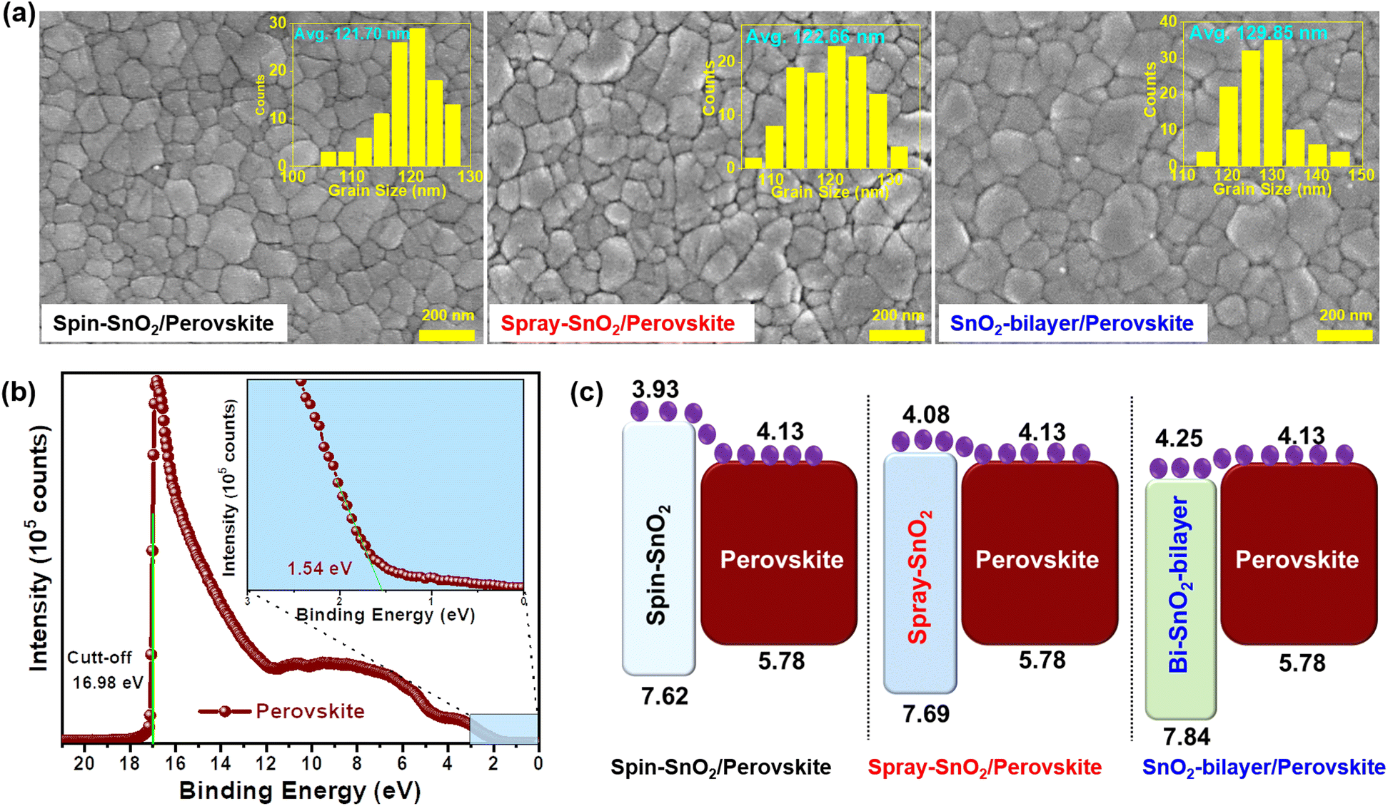 | ||
| Fig. 5 (a) Surface morphologies and grain size distributions (inset) of perovskite films inkjet-printed on different SnO2 ETLs. (b) Ultraviolet photoelectron spectroscopy (UPS) spectra of the perovskite film; the inset shows the onset region. (c) Schematic energy band alignment of inkjet-printed perovskite films with different SnO2 ETLs. | ||
The core-level XPS spectra of Pb 4f, I 3d, Br 3d, C 1s, N 1s, and Cs 3d elements of the inkjet-printed perovskite film over glass substrate are shown in Fig. S2(a).† Generally, Pb 4f spectra consist of two high-intensity Pb 4f7/2 and Pb 4f5/2 peaks that exist at BEs of 138.2 and 143.1 eV, respectively, with a spin–orbital splitting of 4.9 eV. The spectrum of I 3d shows two leading peaks at BEs of 619 and 630.5 eV. Fig. S2(b),† corresponding to the I 3d5/2 and I 3d3/2 components, individually. Fig. S2(c)† illustrates the two dominant peaks of the Br 3d core level spectrum at BEs of 68.3 and 69.2 eV belonging to the Br 3d5/2 and Br 3d3/2, respectively. Similarly, the C 1s and N 1s core-level spectra in Fig. S2(d) and (e)† depict the C![[double bond, length as m-dash]](https://www.rsc.org/images/entities/char_e001.gif) NH2+ at 288.04 and 400.28 eV, respectively. The Cs 3d spectrum in Fig. S2(f)† represents the intensity of the Cs 3d5/2 and Cs 3d3/2 core levels at 724.5 eV and 738.53 eV, respectively. These results confirmed that the inkjet-printed perovskite film has high phase purity.
NH2+ at 288.04 and 400.28 eV, respectively. The Cs 3d spectrum in Fig. S2(f)† represents the intensity of the Cs 3d5/2 and Cs 3d3/2 core levels at 724.5 eV and 738.53 eV, respectively. These results confirmed that the inkjet-printed perovskite film has high phase purity.
The Ecut-off and Eon-set values of the inkjet-printed perovskite film are investigated via UPS measurements. The values of work function (WS), as well as the valence band maximum (EVB) of the inkjet-printed perovskite film, were estimated from Fig. 5b and using Exp. S(1 and 2).† The conduction band maximum (ECB) and band gap values were estimated from Exp. S3† and the Tauc plot, respectively. All these parameters are summarized in Table S2.† The results revealed that the ECB of the SnO2-bilayer ETL had a smaller band offset with the ECB of the perovskite film, which is more beneficial for collecting charges at the SnO2/perovskite interface (Fig. 5c). Meanwhile, an energy barrier of ∼0.05 eV was seen in the ECB value of the spray-SnO2 ETL and the ECB value of the perovskite film, which can impede the interfacial electron transfer. The biggest band offset was observed in the spin-SnO2/perovskite interface, which can cause interfacial recombination of charge carriers and reduce the overall device performance. In addition, the deeper EVB value of the SnO2-bilayer compared to the spin-SnO2 and spray-SnO2 ETLs can help to inhibit recombination at the SnO2/perovskite boundaries, thereby improving the device performance of IJP-PSCs. Overall, these results have confirmed that significant variations have arisen in the elemental composition and band alignment of the SnO2-bilayer/perovskite film, which can lead to considerable changes in the device performance of PSCs.
2.3 Device performance of IJP-PSCs based on different SnO2 ETLs
To investigate the device performance of SnO2 ETLs, we fabricated n-i-p type IJP-PSCs with a device configuration of ITO/SnO2/inkjet-printed perovskite/spiro-OMeTAD/Ag, as schematically illustrated in Fig. 6(a). Fig. 6(b) displays the current density and voltage (J–V) curves of the representative IJP-PSC devices fabricated on spin-SnO2, spray-SnO2, and SnO2-bilayer ETLs, and the detailed device parameters are presented in Table 1. | ||
| Fig. 6 (a) Schematic device architecture of a complete PSC device. (b) J–V characteristic curves, (c) EQE spectra and integrated photocurrent density of PSC devices based on different SnO2 ETLs and inkjet-printed perovskite films. (d) PCE distributions of inkjet-printed PSCs based on different SnO2 ETLs. (e) Comparison of the performance of state-of-the-art IJP-PSCs based on TiO2 and SnO2 ETLs. (f) TRPL spectra of inkjet-printed perovskite films coated on different SnO2 ETLs. | ||
| Device | V oc [V] | J sc [mA cm−2] | J sc (EQE) [mA cm−2] | FF [%] | PCE [%] | Avg. PCE [%] |
|---|---|---|---|---|---|---|
| Spin-SnO2 | 1.168 | 17.92 | 17.89 | 70.56 | 14.77 | 13.48 ± 0.8 |
| Spray-SnO2 | 1.182 | 18.31 | 18.21 | 70.64 | 15.29 | 14.49 ± 0.5 |
| SnO2-bilayer | 1.187 | 18.32 | 18.30 | 77.73 | 16.90 | 15.76 ± 0.5 |
Based on the use of a similar inkjet-printed perovskite film, the device made up of a SnO2-bilayer ETL attained a notably better PCE of ∼16.9% compared to the devices based on spin-SnO2 (PCE ∼14.8%) and spray-SnO2 (PCE ∼15.3%) ETLs. The superior performance of the SnO2-bilayer-based IJP-PSCs is mostly related to the efficient charge transfer between the SnO2/perovskite layers. Suitable band alignment and improved charge transfer at the ETL/perovskite interface can enhance the Voc and FF of the device. SnO2-bilayer-based devices recorded a higher FF of 77.73% compared to those based on spin-SnO2 (FF: 70.56%) and spray-SnO2 (FF: 70.64%). A similar improvement was observed in the Voc of the SnO2-bilayer-based device (Voc: 1.187 V) compared to the devices based on spin-SnO2 (Voc: 1.168 V) and spray-SnO2 (Voc: 1.182 V). The higher Voc of the SnO2-bilayer-based device is attributable to the deeper EVB of the SnO2-bilayer ETL relative to those of the spin-SnO2 and spray-SnO2 ETLs. Overall, in the literature, the PCE of our IJP-PSC devices is the highest amongst the SnO2-based inkjet-printed PSC systems, as shown in Fig. 6(e).10,12,13,26,27,29 The literature survey of the performance of IJP-PSC photovoltaic devices based on different TiO2 and SnO2 ETLs is presented in Table S5.† To provide further insight, electro-optical characterization was performed on IJP-PSC devices. The integrated Jsc values of the devices were estimated from the external quantum efficiency (EQE) spectra in Fig. 6(c). The device based on the SnO2-bilayer exhibited an integrated Jsc value of 18.30 mA cm−2, which matches well with the measured Jsc values obtained from the J–V measurement (Table 1). On another note, we also investigated the long-term stability and photostability of IJP-PSC devices comprising different SnO2. The photostability measurements showed that all three devices generated stable Jsc values over a prolonged one-sun illumination for 500 s (Fig. S5(a)†). Nonetheless, the shelf-life of the IJP-PSCs based on spin-SnO2 and spray-SnO2 was lower than the analogues based on the SnO2-bilayer (Fig. S5(b)†). Moreover, the performance of 20 IJP-PSC devices with different SnO2 ETLs was tested, and confirmed reproducibility data were displayed in a PCE distribution plot in Fig. 6(d). Among all, IJP-PSCs based on the SnO2-bilayer ETL achieved the highest average PCE of (15.76 ± 0.5)%, which clearly shows the highly reproducible performance of the devices. The J–V curves of IJP-PSC devices under forward-scan and reverse-scan are shown in Fig. S4,† and the hysteresis index (HI) of every device was calculated using Expression S4.† The IJP-PSC device made with a SnO2-bilayer showed a considerably lower HI (∼0.001) compared with the spin-SnO2 (∼0.012) and spray-SnO2 (∼0.007), and these low HI values were attributed to the improved SnO2 ETL/perovskite interfacial morphology.25 Furthermore, we fabricated normal PSC devices based on spin-coated perovskite films and tested them under similar conditions. The forward and reverse scan J–V curves are depicted in Fig. S3,† and estimated J–V parameters are described in Table S3.† Using the same SnO2-bilayer ETL, the PCE of the inkjet-printed PSC device (∼16.9%) only showed an ∼0.3% PCE decrease from that of the spin-coated PSC (PCE ∼17.2%). Meanwhile, the devices made with spin-SnO2 and spray-SnO2 showed considerably larger PCE deficit values of ∼2.4% and ∼1.9%. This finding shows that the SnO2-bilayer is a better ETL for IJP-PSCs, and it can also be flexibly used in solution-processed PSCs with different perovskite systems to produce good performance.
To study the charge transport properties between the SnO2 ETL and the inkjet-printed perovskite absorber, we performed transient photoluminescence (TRPL) measurements on the SnO2/perovskite films, and the fluorescence decay lifetimes (τPL) of the samples were estimated using Expression S5†. As presented in Fig. 6(f), the reference inkjet-printed perovskite film (without SnO2) showed the maximum τPL of 54 ns. With the incorporation of SnO2-bilayer, the τPL values of the inkjet-printed perovskite film decreased to 25 ns (Table S4†), signifying a highly effective charge transfer at the SnO2/perovskite interface that contributed positively to the device performance of IJP-PSCs.
3. Conclusion
In summary, we have successfully developed SnO2-bilayer ETLs with better uniformity and a granule-textured surface using a solution-processed spin/spray-coating technique. The SnO2-bilayer ETL displayed a pinhole free nanograin-textured surface that benefitted the printing of the larger grain perovskite overlayer compared with spin-SnO2 and spray-SnO2 films. The device performance of SnO2-bilayer and spray-SnO2 ETLs was investigated using the spin-SnO2 ETL as a reference. The IJP-PSCs made with the SnO2-bilayer ETL and inkjet-printed perovskite film exhibited superior performance with a PCE of ∼16.9%, compared to those of the spin-SnO2 (PCE ∼14.8%) and spray-SnO2 (∼15.3%) analogues. The spray-assisted deposition of SnO2 ETLs and the inkjet-printing of perovskite films under ambient conditions enable the production of large-area photovoltaic devices/modules that are entirely compatible with roll-to-roll (R2R) processing over rigid/flexible electrodes.Author contributions
V. V. S.: conceptualization, visualization, methodology, formal analysis, investigation, and writing – original draft, review and editing. N. K.: methodology, supervision and writing – review and editing. H. B. L.: supervision and writing – review and editing. M. M. O.: methodology, writing – review and editing, and formal analysis. S. C.: methodology and formal analysis. B. T.: methodology and formal analysis. A. M.: formal analysis. J.-W. K.: supervision, funding acquisition, and writing – review and editing.Conflicts of interest
The authors declare no conflict of interest.Acknowledgements
This work was financially supported by the Basic Science Research Program (NRF-2021R1A2C2004206) and the Creative Materials Discovery Program (NRF-2017M3D1A1039287) through the National Research Foundation (NRF) of Korea, funded by the MSIT. This work was supported by the Technology Innovation Program (20016283) funded by the Ministry of Trade, Industry & Energy (MOTIE, Korea). This work was supported by the selection of a research-oriented professor at Jeonbuk National University in 2023.References
- H. Min, D. Y. Lee, J. Kim, G. Kim, K. S. Lee, J. Kim, M. J. Paik, Y. K. Kim, K. S. Kim, M. G. Kim, T. J. Shin and S. Il Seok, Perovskite solar cells with atomically coherent interlayers on SnO2 electrodes, Nature, 2021, 598, 444–450 CrossRef CAS PubMed.
- N. J. Jeon, H. Na, E. H. Jung, T. Y. Yang, Y. G. Lee, G. Kim, H. W. Shin, S. Il Seok, J. Lee and J. Seo, A fluorene-terminated hole-transporting material for highly efficient and stable perovskite solar cells, Nat. Energy, 2018, 3, 682–689 CrossRef CAS.
- M. M. Lee, J. Teuscher, T. Miyasaka, T. N. Murakami and H. J. Snaith, Efficient hybrid solar cells based on meso-superstructured organometal halide perovskites, Science, 2012, 338, 643–647 CrossRef CAS PubMed.
- J. Feng, Y. Jiao, H. Wang, X. Zhu, Y. Sun, M. Du, Y. Cao, D. Yang and S. F. Liu, High-throughput large-area vacuum deposition for high-performance formamidine-based perovskite solar cells, Energy Environ. Sci., 2021, 14, 3035–3043 RSC.
- J. E. Bishop, C. D. Read, J. A. Smith, T. J. Routledge and D. G. Lidzey, Fully spray-coated triple-cation perovskite solar cells, Sci. Rep., 2020, 10, 1–8 CrossRef PubMed.
- J. W. Lee, S. I. Na and S. S. Kim, Efficient spin-coating-free planar heterojunction perovskite solar cells fabricated with successive brush-painting, J. Power Sources, 2017, 339, 33–40 CrossRef CAS.
- F. Schackmar, H. Eggers, M. Frericks, B. S. Richards, U. Lemmer, G. Hernandez-Sosa and U. W. Paetzold, Perovskite solar cells with all-inkjet-printed absorber and charge transport layers, Adv. Mater. Technol., 2021, 6, 2000271 CrossRef CAS.
- B. J. De Gans, P. C. Duineveld and U. S. Schubert, Inkjet printing of polymers: State of the art and future developments, Adv. Mater., 2004, 16, 203–213 CrossRef CAS.
- M. Kuang, L. Wang and Y. Song, Controllable printing droplets for high-resolution patterns, Adv. Mater., 2014, 26, 6950–6958 CrossRef CAS PubMed.
- Z. Wei, H. Chen, K. Yan and S. Yang, Inkjet printing and instant chemical transformation of a CH3NH3PbI3/nanocarbon electrode and interface for planar perovskite solar cells, Angew. Chem., Int. Ed., 2014, 53, 13239–13243 CrossRef CAS PubMed.
- H. Eggers, F. Schackmar, T. Abzieher, Q. Sun, U. Lemmer, Y. Vaynzof, B. S. Richards, G. Hernandez-Sosa and U. W. Paetzold, Inkjet-printed micrometer-thick perovskite solar cells with large columnar grains, Adv. Energy Mater., 2020, 10, 1903184 CrossRef CAS.
- P. Li, C. Liang, B. Bao, Y. Li, X. Hu, Y. Wang, Y. Zhang, F. Li, G. Shao and Y. Song, Inkjet manipulated homogeneous large size perovskite grains for efficient and large-area perovskite solar cells, Nano Energy, 2018, 46, 203–211 CrossRef CAS.
- T. Leijtens, G. E. Eperon, S. Pathak, A. Abate, M. M. Lee and H. J. Snaith, Overcoming ultraviolet light instability of sensitized TiO2 with meso-superstructured organometal tri-halide perovskite solar cells, Nat. Commun., 2013, 4, 1–8 Search PubMed.
- W. Ke, G. Fang, J. Wang, P. Qin, H. Tao, H. Lei, Q. Liu, X. Dai and X. Zhao, Perovskite solar cell with an efficient TiO2 compact film, ACS Appl. Mater. Interfaces, 2014, 6, 15959–15965 CrossRef CAS PubMed.
- S. G. Li, K. J. Jiang, M. J. Su, X. P. Cui, J. H. Huang, Q. Q. Zhang, X. Q. Zhou, L. M. Yang and Y. L. Song, Inkjet printing of CH3NH3PbI3 on a mesoscopic TiO2 film for highly efficient perovskite solar cells, J. Mater. Chem. A, 2015, 3, 9092–9097 RSC.
- J. Ma, Z. Lin, X. Guo, L. Zhou, J. Su, C. Zhang, Z. Yang, J. Chang, S. (Frank) Liu and Y. Hao, Low-temperature solution-processed ZnO electron transport layer for highly efficient and stable planar perovskite solar cells with efficiency over 20%, Sol. RRL, 2019, 3, 1900096 CrossRef.
- C. Chen, Y. Jiang, Y. Wu, J. Guo, X. Kong, X. Wu, Y. Li, D. Zheng, S. Wu, X. Gao, Z. Hou, G. Zhou, Y. Chen, J. M. Liu, K. Kempa and J. Gao, Low-temperature-processed WOx as electron transfer layer for planar perovskite solar cells exceeding 20% efficiency, Sol. RRL, 2020, 4, 1–8 Search PubMed.
- C. Zhang, Y. Shi, S. Wang, Q. Dong, Y. Feng, L. Wang, K. Wang, Y. Shao, Y. Liu and S. Wang, Room-temperature solution-processed amorphous NbOx as an electron transport layer in high-efficiency photovoltaics, J. Mater. Chem. A, 2018, 6, 17882–17888 RSC.
- Q. Luo, H. Chen, Y. Lin, H. Du, Q. Hou, F. Hao, N. Wang, Z. Guo and J. Huang, Discrete Iron(III) oxide nanoislands for efficient and photostable perovskite solar cells, Adv. Funct. Mater., 2017, 27, 1–9 Search PubMed.
- A. P. Muthukrishnan, J. Lee, J. Kim, C. S. Kim and S. Jo, Low-temperature solution-processed SnO2 electron transport layer modified by oxygen plasma for planar perovskite solar cells, RSC Adv., 2022, 12, 4883–4890 RSC.
- K. Neetesh, H. B. Lee, R. Sahani, B. Tyagi, S. Cho, J.-S. Lee and J.-W. Kang, Room-temperature spray deposition of large-area SnO2 electron transport layer for high performance, stable FAPbI3-based perovskite solar cells, Small Methods, 2022, 6, 2101127 CrossRef PubMed.
- H. B. Lee, M.-K. Jeon, N. Kumar, B. Tyagi and J.-W. Kang, Boosting the efficiency of SnO2-triple cation perovskite system beyond 20% using nonhalogenated antisolvent, Adv. Funct. Mater., 2019, 29, 1903213 CrossRef.
- J. Xie, K. Huang, X. Yu, Z. Yang, K. Xiao, Y. Qiang, X. Zhu, L. Xu, P. Wang, C. Cui and D. Yang, Enhanced electronic properties of SnO2 via electron transfer from graphene quantum dots for efficient perovskite solar cells, ACS Nano, 2017, 11, 9176–9182 CrossRef CAS PubMed.
- Y. Lee, S. Paek, K. T. Cho, E. Oveisi, P. Gao, S. Lee, J. S. Park, Y. Zhang, R. Humphry-Baker, A. M. Asiri and M. K. Nazeeruddin, Enhanced charge collection with passivation of the tin oxide layer in planar perovskite solar cells, J. Mater. Chem. A, 2017, 5, 12729–12734 RSC.
- H. B. Lee, N. Kumar, M. M. Ovhal, Y. J. Kim, Y. M. Song and J.-W. Kang, Dopant-free, amorphous–crystalline heterophase SnO2 electron transport bilayer enables >20% efficiency in triple-cation perovskite solar cells, Adv. Funct. Mater., 2020, 30, 2001559 CrossRef CAS.
- A. J. Huckaba, O. Lee, R. Xia, S. Paek, V. C. Bassetto, E. Oveisi, A. Lesch, S. Kinge, P. J. Dyson, H. Girault and N. M. Khaja, Inkjet-printed mesoporous TiO2 and perovskite layers for high efficiency perovskite solar cells, Energy Technol., 2019, 7, 317–324 CrossRef CAS.
- Z. Li, P. Li, G. Chen, Y. Cheng, X. Pi, X. Yu, D. Yang, L. Han, Y. Zhang and Y. Song, Ink engineering of inkjet printing perovskite, ACS Appl. Mater. Interfaces, 2020, 12, 39082–39091 CrossRef CAS PubMed.
- A. Verma, D. Martineau, S. Abdolhosseinzadeh, J. Heier and F. Nüesch, Inkjet printed mesoscopic perovskite solar cells with custom design capability, Mater. Adv., 2020, 1, 153–160 RSC.
- C. S. Pathak, G. Paramasivam, F. Mathies, K. Hirselandt, V. Schröder, O. Maus, J. Dagar, C. Klimm, E. Unger and I. Visoly-Fisher, PTB7 as an Ink-additive for spin-coated versus inkjet-printed perovskite solar cells, ACS Appl. Energy Mater., 2022, 5, 4085–4095 CrossRef CAS.
- J. Chung, S. S. Shin, K. Hwang, G. Kim, K. W. Kim, D. S. Lee, W. Kim, B. S. Ma, Y.-K. Kim, T.-S. Kim and J. Seo, Record-efficiency flexible perovskite solar cell and module enabled by a porous-planar structure as an electron transport layer, Energy Environ. Sci., 2020, 13, 4854 RSC.
- H. B. Lee, R. T. Ginting, S. T. Tan, C. H. Tan, A. Alshanableh, H. F. Oleiwi, C. C. Yap, M. H. H. Jumali and M. Yahaya, Controlled defects of fluorine-incorporated ZnO nanorods for photovoltaic enhancement, Sci. Rep., 2016, 6, 1–11 CrossRef PubMed.
- L. Q. Xie, L. Chen, Z. A. Nan, H. X. Lin, T. Wang, D. P. Zhan, J. W. Yan, B. W. Mao and Z. Q. Tian, Understanding the cubic phase stabilization and crystallization kinetics in mixed cations and halides perovskite single crystals, J. Am. Chem. Soc., 2017, 139, 3320–3323 CrossRef CAS PubMed.
- H. Eggers, F. Schackmar, T. Abzieher, Q. Sun, U. Lemmer, Y. Vaynzof, B. S. Richards, G. Hernandez-Sosa and U. W. Paetzold, Inkjet–printed micrometer–thick perovskite solar cells with large columnar grains, Adv. Energy Mater., 2020, 10, 1903184 CrossRef CAS.
- H. B. Lee, N. Kumar, V. Devaraj, B. Tyagi, S. He, R. Sahani, K.-J. Ko, J.-W. Oh and J.-W. Kang, Trifluoromethyl-group bearing, hydrophobic bulky cations as defect passivators for highly efficient, stable perovskite solar cells, Sol. RRL, 2021, 5, 2100712 CrossRef CAS.
- T. I. Alanazi, O. S. Game, J. A. Smith, R. C. Kilbride, C. Greenland, R. Jayaprakash, K. Georgiou, N. J. Terrill and D. G. Lidzey, Potassium iodide reduces the stability of triple-cation perovskite solar cells, RSC Adv., 2020, 10, 40341–40350 RSC.
- B. Tyagi, H. B. Lee, N. Kumar, W. Y. Jin, K. J. Ko, M. M. Ovhal, R. Sahani, H. J. Chung, J. Seo and J. W. Kang, High-performance, large-area semitransparent and tandem perovskite solar cells featuring highly scalable a-ITO/Ag mesh 3D top electrodes, Nano Energy, 2022, 95, 106978 CrossRef CAS.
- A. S. Marques, R. M. Faria, J. N. Freitas and A. F. Nogueira, Low-Temperature Blade-Coated Perovskite Solar Cells, Ind. Eng. Chem. Res., 2021, 60, 7145–7154 CrossRef CAS.
- X. Wang, L.-L. Deng, L.-Y. Wang, S.-M. Dai, Z. Xing, X.-X. Zhan, X.-Z. Lu, S.-Y. Xie, R.-B. Huang and L.-S. Zheng, Cerium oxide standing out as electron transport layer for efficient and stable perovskite solar cells processed in lowtemperature, J. Mater. Chem. A, 2017, 5, 1706–1712 RSC.
Footnote |
| † Electronic supplementary information (ESI) available: Experimental, Fig. S1–S5, and Tables S1–S5. See DOI: https://doi.org/10.1039/d3qi00599b |
| This journal is © the Partner Organisations 2023 |