
 Open Access Article
 This Open Access Article is licensed under a
 Creative Commons Attribution 3.0 Unported Licence
Nesting-like band gap in bismuth sulfide Bi2S3†
W. M.
Linhart
 *,
S. J.
Zelewski
,
P.
Scharoch
,
F.
Dybała
and
R.
Kudrawiec
*,
S. J.
Zelewski
,
P.
Scharoch
,
F.
Dybała
and
R.
Kudrawiec
Department of Semiconductor Materials Engineering, Faculty of Fundamental Problems of Technology, Wrocław University of Science and Technology, Wybrzeże Wyspiańskiego 27, 50-370 Wrocław, Poland. E-mail: wojciech.linhart@pwr.edu.pl
First published on 31st August 2021
Abstract
The van der Waals material Bi2S3 is a potential solar absorber, but its optoelectronic properties are not fully explored and understood. Here, using theoretical calculations and various experimental techniques under different temperature and hydrostatic pressure conditions, the optoelectronic properties of Bi2S3 are determined. The fundamental absorption edge and photoreflectance transition value has been found to be ∼1.30 eV at room temperature, which is the optimum value, giving a maximum solar cell power conversion efficiency according to the Shockley–Queisser limit for a single-junction solar cell. Temperature-dependent measurements reveal that the total energy change of the fundamental gap between 20 and 300 K is significant at ∼0.16 eV, compared to conventional semiconductors. Theoretical predictions show that Bi2S3 possesses an indirect band gap with the band nesting surrounding. The combination of experimental methods such as photoreflectance, absorption, and photoluminescence clearly shows that the direct optical transition dominates above the indirect one. Therefore, we reveal Bi2S3 as a nesting-like band gap semiconductor with a strong absorption edge and excitonic emission.
1. Introduction
One of the most important scientific fields and a part of the global energy economy is photovoltaics. Nowadays, conventional solar cells are based on three-dimensional crystals of Si, Cu(In,Ga)–Se2 or CdTe and exhibit high device efficiency and stability. However, from a production and environmental perspective, these materials have some problems. For example, the growth of high-quality silicon is energy-intensive and provides environmentally damaging waste products; indium and tellurium are expensive and scarce, while cadmium is a toxic element with restricted use.1–3 Additionally, any imperfection of a three-dimensional crystal can lead to a reduction in device performance via recombination losses. The energy generated from environmentally friendly, cost-effective solar cells is a key aspect for developing a clean renewable energy economy. Therefore, non-toxic and earth-abundant materials with high absorption coefficient and optimal band gap (1–1.7 eV) have received great attention as photovoltaic absorbers.Bi2S3 (bismuth sulfide) is a nontoxic metal chalcogenide semiconductor, which lies in the optimum of the solar spectrum with a band gap varying in the range from 1.3 to 1.7 eV, without conclusive evidence of the origins of this deviation.4,5 Furthermore, Bi2S3 has a high absorption coefficient and a conversion efficiency from an incident photon to electron value of ∼5%.6,7 Under ambient conditions, bismuth sulfide has an orthorhombic structure. The Pnma phase, in which Bi2S3 is being characterized, can be described as a layered (lamellar) structure that allows exfoliation down to monolayers using standard mechanical exfoliation techniques. Different orientations of Bi2S3 are shown in Fig. 1. Substituting sulfur in Bi2S3 with tellurium (Bi2Te3) or selenium (Bi2Se3) changes the structural class of the material into rhombohedral and the electronic properties from semiconductor to topological insulator.8,9 As Bi2Te3 and Bi2Se3 compounds have been studied extensively, Bi2S3 has not received similar attention. Most studies on Bi2S3 are about thermoelectric properties, structural studies and theoretical band structures under different pressure conditions, while comprehensive optical investigations are scarce.10
 | ||
| Fig. 1 Different crystal orientations for Bi2S3. Directions [001], [010], [100] are pointing out of the page in panels (a)–(c), respectively. In panel (b), the layered structure can be observed clearly, and the van der Waals interactions between these layers can be distinguished. | ||
In the present work, temperature-dependent optical absorption and photoreflectance, excitation power-dependent photoluminescence, and hydrostatic pressure-dependent photoreflectance combined with first-principles calculations based on density functional theory have been performed to characterize the optical properties of the bulk Bi2S3. The combination of these techniques has concluded that Bi2S3 is a quasi-direct semiconductor. Moreover, temperature-dependent studies have shown that the total change of the band gap energy is surprisingly enormous in comparison to conventional semiconductors.
2. Experimental and computational details
Bismuth sulfide was investigated by optical absorption, photoreflectance (PR) and photoluminescence (PL) measurements in the temperature range from 20 to 300 K and in the hydrostatic pressure range from 0 to 20 kbar. The samples were illuminated using a halogen lamp and the reflected light was dispersed using a 0.55 m focal length single-grating monochromator. The signal was detected with a Si photodiode and was measured using the lock-in technique. For PR experiments, reflectivity was modulated by a chopped (280 Hz) laser beam of a wavelength of 405 nm. For PR measurements at high hydrostatic pressures, the sample was mounted inside a UNIPRESS piston cylinder-type cell. The chosen pressure hydrostatic medium was Daphne 7474, which remained hydrostatic and transparent during the whole experiment, up to a pressure of 18 kbar. The pressure was determined by measuring the resistivity of the InSb gauge by the four-probe method.11 Photoluminescence measurements were performed in the micro-regime, where a 532 nm line of a diode-pumped solid state laser (DPSS) was focused on the sample by a long working distance objective (50 × magnification, NA = 0.55); the diameter of the laser spot was estimated to be below 2 μm. PL spectra were measured using a single-grating 0.55 m focal length monochromator with a multichannel liquid nitrogen cooled Si CCD array detector. For PL measurements, the samples were mounted on a cold finger in a closed-cycle refrigerator coupled with a programmable temperature controller allowing measurements in the temperature range from 10 to 300 K.The bulk Bi2S3 crystal for this study was obtained from 2D Semiconductors company (USA). The sample was grown using the Bridgman technique. No special sample treatment was performed prior to the measurements. The sample used here was of macroscopic size (∼ 3 × 6 mm with a thickness of ∼0.5 mm) and its purity represents the current state of the art at the manufacturer's facility (99.9999%).
DFT calculations were performed with the use of ABINIT code.12 Scalar relativistic PAW datasets13 with the GGA (PBE) approximation14 (as provided in the ABINIT web page) were used for geometric optimization along with the D-3 correction for the van der Waals interaction.15 Geometrical parameters were optimized for interatomic forces lower than 10−8 Hartree per Bohr. HGH pseudopotentials16 with spin–orbit interactions included were used for the band structure calculations. The MBJLDA functional, which consists of the modified Becke–Johnson exchange potential combined with LDA correlation, has been used.17,18 For the band structure convergence criteria, we took a tolerance on the wave function squared residual of 10−8 and the 3 × 9 × 3 Monkhorst–Pack mesh,19 which was doubled for the DOS calculations. The plane wave basis energy cutoff values of 30 Ha for geometric optimization and 40 Ha for band structure calculations were used.
3. Results and discussion
Because of the previously reported properties of bismuth sulfide, scientists still debate whether this material has a direct or indirect band-gap. Here, we present that the bulk bismuth sulfide is rather a quasi-direct band-gap semiconductor. Fig. 2 shows PR, absorption, and PL spectra for Bi2S3 acquired at 80 K. Combining these experimental techniques allows the unambiguous determination of the nature of the Bi2S3 optical transition and the establishment of its energy. Since PR is only sensitive to direct optical transitions and the PR resonance covers the absorption and PL spectra, we can conclude that all the presented measurements here reveal the direct character of the optical transition. In order to determine the position of the resonance in the energy scale and its broadening, the PR spectrum was fitted using Aspnes formula: | (1) |
 denotes the energy dependence of the PR signal, A is the amplitude of the resonance, Et indicates the energy of the optical transition, Γ is the broadening parameter and θ represents the phase of the resonance line.20 The parameter m depends on the character of the optical transition; m = 2.5 is conventionally used for the band-to-band transition, while m = 2 is assigned for the excitonic transition. For better illustration of the energy transition, its modulus is plotted in Fig. 2 below the PR spectrum (see the peak with a dashed line envelope at the bottom), which is defined as
 | (2) |
 | ||
| Fig. 2 Photoreflectance, optical absorption, and photoluminescence spectra of Bi2S3 measured at 80 K. Aspnes fit to the PR spectrum is also included, and the modulus of the PR transition is plotted at the bottom. | ||
In the case of the photoluminescence spectrum, we can observe a strong emission signal of E = 1.43 eV at 80 K, which corresponds well to the PR resonance and the absorption edge. In addition, one can note a small broad peak emission near 1.25 eV, which we can assign to the defect-like emission.21
The temperature dependence of the optical transition of Bi2S3 has also been comprehensively investigated. For this purpose, PR and absorption measurements have been performed in the temperature range from 10 to 280 K. Fig. 3(a) shows PR spectra and corresponding fits of Bi2S3 measured at temperatures between 20 and 300 K. The transition energy at each temperature was determined by fitting the spectra with eqn (1). It can be observed that the position of the PR resonance moves toward lower energies and broadens as the temperature increases. The temperature evolution of the PR broadening parameter is shown in Fig. 3(b) and it should be arranged according to the Bose–Einstein relation
 | (3) |
 | ||
| Fig. 3 (a) Temperature dependence of photoreflectance spectra with Aspnes fits (dashed lines) for Bi2S3. (b) Temperature dependence of the broadening parameter for Bi2S3 with the fit by the Bose–Einstein formula (red dashed line). (c) Temperature-dependent absorption of Bi2S3. (d) Temperature dependence of the band gap for Bi2S3. Open circles are results obtained from absorption measurements, while closed circles are results obtained from photoreflectance. Dashed lines indicate Varshni fits, while the solid line indicates the Bose–Einstein fit. | ||
The absorption spectra obtained at different temperatures for Bi2S3 are shown in Fig. 3(c). The absorption onsets vary between 1.30 at 300 K and 1.45 eV at 10 K. This optical characteristic suggests a maximum solar cell power conversion efficiency of 32.57% based on the Shockley–Queisser limit for a single-junction solar cell.23,24 The absorption coefficient, α, rapidly increases to 1 × 104 cm−1 (1 × 108 cm−2 for α2) above each onset, a value typical of direct band gap semiconductors. The plots of α2versus photon energy exhibit an approximately linear behaviour, which is again consistent with a direct band gap. No features below the sharp onset of α were observed that would be a strong indication of an indirect transition. Additionally, we also performed photoacoustic spectroscopy (PAS) (shown with experimental details in Fig. S1 in the ESI†), which is very sensitive for the indirect and the direct transitions;25 no evidence of the indirect-like band gap was observed.
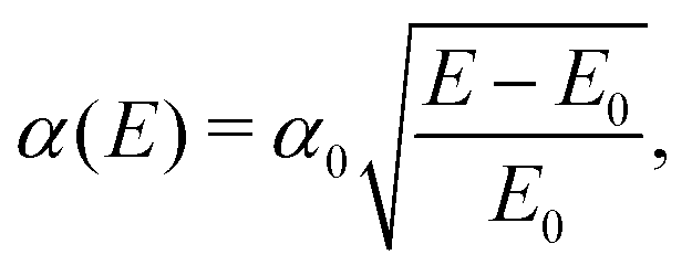
The α0 parameter values, which can be considered as a measure of the absorption strength, were found to be 8.5 × 104 cm−1 and 7.1 × 104 cm−1 at 10 K and 300 K, respectively. These values are comparable with the α0 parameter values observed in direct gap III–V semiconductors.26 The α0 value has been determined from the fits by the formula
 | (4) |
The temperature dependencies of optical transition energy are plotted in Fig. 3(d). Filled green circles denote the results obtained from PR and Aspnes fitting, while open blue circles represent the results obtained from optical absorption, where values were found using standard linear extrapolation to the background intensity of α2versus hν curves. The temperature dependence of the optical transition has been approximated by both a commonly used semi-empirical Varshni relation (dashed lines) and a relation derived from the Bose–Einstein (B–E) statistics (solid grey lines). The Varshni relation is given by
 | (5) |
 | (6) |
Fig. 4(a–c) display the PL spectra recorded at 11 K, 100 K and 200 K and various continuous wave laser excitation power (Pexc) values ranging from 0.22 to 8.2 mW. PL emission bands have been spectrally integrated to evaluate the overall emission intensity (I) as a function of Pexc. The outcome is plotted in the log–log scale as shown in Fig. 4(d). Experimental points have been fitted to the power law function of I∝Pγexc (solid lines in Fig. 4(d)), where γ depends on the radiative recombination process.36 When the majority of the photo-injected electron–hole (e–h) population recombines via the defect states of donors or acceptors, then γ <1. However, when the e–h recombination takes over the defect-related emission and the nature of the emission is excitonic, then γ ≈ 1. γ = 2 indicates a band-to-band recombination. For the considered sample, the fitting procedures have yielded γ = 1.11 ± 0.01 and 1.26 ± 0.01. The results suggest that the PL response arises mainly from the emission of excitons with a negligible impact of defect-related recombination processes. Moreover, γ = 1.11 ± 0.01 at 200 K suggests a high binding energy of excitons. The shift of the PL maximum to lower energies with increasing excitation power can be observed (Fig. 4(a–c)); this is a result of additional heating that comes from the laser illumination of the sample.
 | ||
| Fig. 4 Excitation power-dependent PL spectra taken at (a)11 K, (b) 100 K, and (c) 200 K. (d) Integrated intensity of the PL emission band for Bi2S3 as a function of the excitation power (Pexc). | ||
We also performed high-pressure PR measurements to determine the nature of optical transitions based on the expected differences in the pressure coefficients of optical transitions at different points of the Brillouin Zone.37–39 The PR spectra obtained at different hydrostatic pressures are shown in Fig. 5(a). As it can be observed in the figure, two PR features show up at 4.46 kbar at E1 ≈ 1.28 eV and E2 ≈ 1.39 eV, whose energies decrease upon the applied pressure. It should be noted that the transition E2 has not been observed during PR temperature-dependent measurements, although it clearly appears above the pressure of 2.88 kbar of hydrostatic pressure. In order to recognize the origin of the observed optical transitions, the band structure calculations for different hydrostatic pressures have been performed. The calculated electronic band structure along the principal high-symmetry directions is shown in Fig. 5(b) for zero pressure (black lines) and 20 kbar (red-dashed lines). These calculations predict the valence band maximum (VBM) of ribbon-like Bi2S3 taking place between Γ and X points, while the conduction band minimum (CBM) at the Γ point resulting in the indirect band gap of ∼1.23 eV for 0 kbar and ∼1.09 eV for 20 kbar. This is in good agreement with previously reported values.5,40–44 The indirect band gap is indicated by the gray arrow in Fig. 5(b). The transition E1, which takes place at non-high symmetry k points with an enhanced joint density, is a band-nesting transition. The energy difference dispersion of the bands between optical transitions occuring at the nesting region should be flat (see Fig. S3 in the ESI†). This kind of transition has previously been reported in the other families of layered compounds such as TMDs.45,46 The E2 transition observed in hydrostatic pressure-dependent spectra is assigned to the transition between the third valence band below 0 eV and the conduction band at the Γ point as the calculated matrix elements suggest (see Fig. S4 in the ESI†).
 | ||
| Fig. 5 (a) Hydrostatic pressure dependence of photoreflectance spectra with Aspnes fits (dashed lines) for Bi2S3, which is obtained at 290 K. (b) Calculated band structure for Bi2S3 at 0 kbar and 20 kbar hydrostatic pressure. (c) Hydrostatic pressure dependence of the PR transitions for Bi2S3. Circles are the results obtained from PR measurements at 290 K, while diamonds are the results obtained from DFT calculations. Solid lines indicate linear fits of the PR results to obtain hydrostatic pressure coefficients. | ||
Fig. 5(c) shows the changes of transitions E1 and E2 as a function of the hydrostatic pressure together with theoretical predictions. It is clearly visible that the agreement between experimental data and theoretical predictions is good. The hydrostatic pressure coefficient values obtained from PR measurements are −5.5 ± 0.2 meV kbar−1 for E1 and −7.1 ± 0.3 meV kbar−1 for E2, while DFT calculations give −9.2 meV kbar−1 and −6.1 meV kbar−1, respectively. The good agreement between pressure coefficients determined experimentally and theoretically indicates that the nature of these transitions is interpreted appropriately. This leads to the conclusion that the electronic band structure determined by DFT calculations is correct, and the fundamental band gap is indirect, while the direct character of the band gap observed in optical measurements comes from band nesting. Therefore, the observed PL emission has an excitonic character, and a strong absorption coefficient is observed for the absorption edge.
4. Conclusions
Theoretical calculations show that Bi2S3 has an indirect band gap, but its character is different from Si or other well-known indirect gap semiconductors. Experimental studies (photoreflectance and absorption) presented here suggest its direct character. Furthermore, photoluminescence and hydrostatic pressure-dependent PR measurements confirm the direct-like character of the band gap. A careful analysis of the band structure shows us that the experimental results are very consistent with the DFT calculations. It has been found that the band structure has a region with the same slopes of the conduction and valence bands, near the Γ point of the Brillouin zone. This allows for quasi-direct transition which dominates in optical experiments. Therefore, Bi2S3 is a rather unique semiconductor possessing nesting-like band gap nature. Temperature-dependent measurements have shown that the total energy change value of the fundamental gap between 10 and 300 K is significant at ∼0.16 eV, compared with conventional semiconductors. The nesting-like band gap value has been found to be ∼1.30 eV at room temperature, which is the optimum value, giving a maximum solar cell power conversion efficiency according to the SQ limit. The absorption coefficient α0 value has been found to be 8.5 × 104 cm−1, which is comparable with the absorption coefficient observed in direct gap III–V semiconductors. Thus, we expect that Bi2S3 can be useful for engineering environmentally friendly solar cells.Conflicts of interest
There are no conflicts to declare.Acknowledgements
W. M. L. acknowledges support from the Polish National Science Center (Grant No. 2019/35/B/ST5/02819). S. J. Z. is a beneficiary of the START scholarship from the Foundation for Polish Science.References
- C. Candelise, M. Winskel and R. Gross, Prog. Photovolt.: Res. Appl., 2012, 20, 816 CrossRef.
- H. Yang, X. Huang and J. R. Thompson, Nature, 2014, 509, 563 CrossRef PubMed.
- S. Battersby, Proc. Natl. Acad. Sci. U. S. A., 2019, 116, 7 CrossRef CAS.
- M. Khadraoui, N. Benramdane, R. Miloua, C. Mathieu, A. Bouzidi and K. Sahraoui, Optoelectron. Adv. Mater., Rapid Commun., 2015, 9, 1167 CAS.
- M. R. Filip, C. E. Patrick and F. Giustino, Phys. Rev. B: Condens. Matter Mater. Phys., 2013, 87, 205125 CrossRef.
- L. M. Peter, K. G. U. Wijayantha, D. J. Riley and J. P. Waggett, J. Phys. Chem. B, 2003, 107, 8378 CrossRef CAS.
- G. Konstantatos, L. Levina, J. Tang and E. H. Sargent, Nano Lett., 2008, 8, 4002 CrossRef CAS PubMed.
- Y. L. Chen, J. G. Analytis, J.-H. Chu, Z. K. Liu, S.-K. Mo, X. L. Qi, H. J. Zhang, D. H. Lu, X. Dai, Z. Fang, S. C. Zhang, I. R. Fisher, Z. Hussain and Z.-X. Shen, Science, 2009, 325, 178 CrossRef CAS.
- H. Zhang, C.-X. Liu, X.-L. Qi, X. Dai, Z. Fang and S.-C. Zhang, Nat. Phys., 2009, 5, 438 Search PubMed.
- R. Chmielowski, D. Péré, C. Bera, I. Opahle, W. Xie, S. Jacob, F. Capet, P. Roussel, A. Weidenkaff, G. K. H. Madsen and G. Dennler, J. Appl. Phys., 2015, 117, 125103 CrossRef.
- R. Kudrawiec and J. Misiewicz, Appl. Surf. Sci., 2006, 253, 80 CrossRef CAS.
- X. Gonze, F. Jollet, F. A. Araujo, D. Adams, B. Amadon, T. Applencourt, C. Audouze, J.-M. Beuken, J. Bieder, A. Bokhanchuk, E. Bousquet, F. Bruneval, D. Caliste, M. Côté, F. Dahm, F. D. Pieve, M. Delaveau, M. D. Gennaro, B. Dorado, C. Espejo, G. Geneste, L. Genovese, A. Gerossier, M. Giantomassi, Y. Gillet, D. Hamann, L. He, G. Jomard, J. L. Janssen, S. L. Roux, A. Levitt, A. Lherbier, F. Liu, I. Lukačević, A. Martin, C. Martins, M. Oliveira, S. Poncé, Y. Pouillon, T. Rangel, G.-M. Rignanese, A. Romero, B. Rousseau, O. Rubel, A. Shukri, M. Stankovski, M. Torrent, M. V. Setten, B. V. Troeye, M. Verstraete, D. Waroquiers, J. Wiktor, B. Xu, A. Zhou and J. Zwanziger, Comput. Phys. Commun., 2016, 205, 106 CrossRef CAS.
- P. E. Blöchl, Phys. Rev. B: Condens. Matter Mater. Phys., 1994, 50, 17953 CrossRef PubMed.
- J. P. Perdew, K. Burke and M. Ernzerhof, Phys. Rev. Lett., 1996, 77, 3865 CrossRef CAS PubMed.
- S. Grimme, J. Antony, S. Ehrlich and H. Krieg, J. Chem. Phys., 2010, 132, 154104 CrossRef PubMed.
- J. P. Perdew and Y. Wang, Phys. Rev. B: Condens. Matter Mater. Phys., 1992, 45, 13244 CrossRef PubMed.
- J. A. Camargo-Martínez and R. Baquero, Phys. Rev. B: Condens. Matter Mater. Phys., 2012, 86, 195106 CrossRef.
- F. Tran and P. Blaha, Phys. Rev. Lett., 2009, 102, 226401 CrossRef PubMed.
- H. J. Monkhorst and J. D. Pack, Phys. Rev. B: Solid State, 1976, 13, 5188 CrossRef.
- D. Aspnes, Surf. Sci., 1973, 37, 418 CrossRef CAS.
- D. Han, M.-H. Du, C.-M. Dai, D. Sun and S. Chen, J. Mater. Chem. A, 2017, 5, 6200 RSC.
- P. Lautenschlager, P. B. Allen and M. Cardona, Phys. Rev. B: Condens. Matter Mater. Phys., 1986, 33, 5501 CrossRef CAS PubMed.
- W. Shockley and H. J. Queisser, J. Appl. Phys., 1961, 32, 510 CrossRef CAS.
- S. Rühle, Sol. Energy, 2016, 130, 139 CrossRef.
- S. J. Zelewski and R. Kudrawiec, Sci. Rep., 2017, 7, 15365 CrossRef PubMed.
- M. Bhowmick, H. Xi and B. Ullrich, Materials, 2021, 14, 1639 CrossRef CAS PubMed.
- J. I. Pankove, Optical Processes in Semiconductors, Dover Publications, New York, NY, USA, 2nd edn, 1971 Search PubMed.
- Y. Varshni, Physica, 1967, 34, 149 CrossRef CAS.
- L. Viña, S. Logothetidis and M. Cardona, Phys. Rev. B: Condens. Matter Mater. Phys., 1984, 30, 1979 CrossRef.
- I. Zumeta-Dubé, J.-L. Ortiz-Quiñonez, D. Díaz, C. Trallero-Giner and V.-F. Ruiz-Ruiz, J. Phys. Chem. C, 2014, 118, 30244 CrossRef.
- P. A. E. Murgatroyd, M. J. Smiles, C. N. Savory, T. P. Shalvey, J. E. N. Swallow, N. Fleck, C. M. Robertson, F. Jäckel, J. Alaria, J. D. Major, D. O. Scanlon and T. D. Veal, Chem. Mater., 2020, 32, 3245 CrossRef CAS.
- A. Tołłoczko, R. Oliva, T. Woźniak, J. Kopaczek, P. Scharoch and R. Kudrawiec, Mater. Adv., 2020, 1, 1886 RSC.
- M. Sigiro, Y.-S. Huang, C.-H. Ho, Y.-C. Lin and K. Suenaga, Jpn. J. Appl. Phys., 2015, 54, 04DH05 CrossRef.
- A. Arora, M. Koperski, K. Nogajewski, J. Marcus, C. Faugeras and M. Potemski, Nanoscale, 2015, 7, 10421 RSC.
- I. Vurgaftman, J. R. Meyer and L. R. Ram-Mohan, J. Appl. Phys., 2001, 89, 5815 CrossRef CAS.
- T. Schmidt, K. Lischka and W. Zulehner, Phys. Rev. B: Condens. Matter Mater. Phys., 1992, 45, 8989 CrossRef PubMed.
- F. Dybała, M. P. Polak, J. Kopaczek, P. Scharoch, K. Wu, S. Tongay and R. Kudrawiec, Sci. Rep., 2016, 6, 26663 CrossRef.
- R. Oliva, M. Laurien, F. Dybala, J. Kopaczek, Y. Qin, S. Tongay, O. Rubel and R. Kudrawiec, npj 2D Mater. Appl., 2019, 3, 20 CrossRef.
- R. Oliva, T. Woźniak, F. Dybala, J. Kopaczek, P. Scharoch and R. Kudrawiec, Mater. Res. Lett., 2020, 8, 75 CrossRef CAS.
- P. Larson, V. A. Greanya, W. C. Tonjes, R. Liu, S. D. Mahanti and C. G. Olson, Phys. Rev. B: Condens. Matter Mater. Phys., 2002, 65, 085108 CrossRef.
- H. Koc, H. Ozisik, E. Deligöz, A. M. Mamedov and E. Ozbay, J. Mol. Model., 2014, 20, 2180 CrossRef.
- E. Zahedi, Superlattices Microstruct., 2015, 81, 49 CrossRef CAS.
- T. Pandey and A. K. Singh, J. Mater. Chem. C, 2016, 4, 1979 RSC.
- Y. Chen, D. Wang, Y. Zhou, Q. Pang, J. Shao, G. Wang, J. Wang and L.-D. Zhao, Front. Phys., 2018, 14, 13601 CrossRef.
- A. Carvalho, R. M. Ribeiro and A. H. Castro, Neto, Phys. Rev. B: Condens. Matter Mater. Phys., 2013, 88, 115205 CrossRef.
- J. Kopaczek, M. P. Polak, P. Scharoch, K. Wu, B. Chen, S. Tongay and R. Kudrawiec, J. Appl. Phys., 2016, 119, 235705 CrossRef.
Footnote |
| † Electronic supplementary information (ESI) available. See DOI: 10.1039/d1tc03625d |
| This journal is © The Royal Society of Chemistry 2021 |