
 Open Access Article
 This Open Access Article is licensed under a
 Creative Commons Attribution 3.0 Unported Licence
Field emission and anode etching during formation of length-controlled nanogaps in electrical breakdown of horizontally aligned single-walled carbon nanotubes†
Keigo
Otsuka
a,
Taiki
Inoue
*a,
Yuki
Shimomura
a,
Shohei
Chiashi
a and
Shigeo
Maruyama
*ab
aDepartment of Mechanical Engineering, The University of Tokyo, Tokyo 113-8656, Japan. E-mail: inoue@photon.t.u-tokyo.ac.jp; maruyama@photon.t.u-tokyo.ac.jp
bEnergy NanoEngineering Lab., National Institute of Advanced Industrial Science and Technology (AIST), Ibaraki 305-8564, Japan
First published on 18th August 2016
Abstract
We observe field emission between nanogaps and voltage-driven gap extension of single-walled carbon nanotubes (SWNTs) on substrates during the electrical breakdown process. Experimental results show that the gap size is dependent on the applied voltage and humidity, which indicates high controllability of the gap size by appropriate adjustment of these parameters in accordance with the application. We propose a mechanism for the gap formation during electrical breakdown as follows. After small gaps are formed by Joule heating-induced oxidation, SWNTs on the anode side are electrochemically etched due to physically-adsorbed water from the air and the enhanced electric field at the SWNT tips. Field emission is measured in a vacuum as a possible mechanism for charge transfer at SWNT gaps. The relationship between the field enhancement factor and geometric features of SWNTs explains both the voltage dependence of the extended gap size and the field emission properties of the SWNT gaps. In addition, the similar field-induced etching can cause damage to adjacent SWNTs, which possibly deteriorates the selectivity for cutting metallic pathways in the presence of water vapor.
Introduction
Electrical breakdown1 of single-walled carbon nanotubes (single-walled CNTs, SWNTs) has been performed to selectively cut metallic SWNTs (m-SWNTs) for field-effect transistor (FET) applications,2–5 or to create SWNT nanogaps for use as nanoscale electrodes6–8 to contact single molecules9,10 and functional materials.11 When a high bias voltage is applied across SWNTs, the SWNTs are physically cut at the hottest points due to self-heating-induced oxidation,12,13 and become electrically insulating due to formation of the gap. Electrical breakdown has been widely applied to both SWNTs on substrates and suspended over trenches10,14 because it is an extremely simple operation.However, even limited to individual SWNTs on substrates, the size of nanogaps (Lgap) obtained from electrical breakdown varies widely from ca. 2 nm15 to more than 100 nm.11 The reason for the wide variation of the gap size has not been fully explained, even though the mechanism of gap formation seems simple. Instead, gap formation of multi-walled CNTs (MWNTs) and SWNT bundles has been observed in more detail, despite the more complicated processes involved with the layer-by-layer oxidation of multiple shells.1,12,16–18 For any application, the gap size has a significant effect on the device performance and should thus be carefully controlled. For example, nanogaps in the SWNT array channels of SWNT-FETs amplify and localize the electric field and could result in a correlated breakdown of neighboring SWNTs.19,20 The extent to which the field is amplified is highly dependent on the nanogap size; therefore, the gap size should be designed in accordance with the device requirements. On the other hand, phase change memory devices that employ SWNTs as electrodes11 require smaller gaps to achieve higher energy efficiency. There is a lack of detailed understanding on the formation mechanisms of SWNT gaps; however, the controllability of the nanogap size has been reported to a limited extent; a shorter distance between two metallic contacts (SWNT length or channel length; Lch) or breakdown in the Ar gas flow results in smaller nanogaps,11,15 although there has been little explanation of the reason for the small gap formation.
In this work, we report the voltage-driven gap extension phenomenon of SWNTs after electrical breakdown. It is generally considered that SWNTs cut by electrical breakdown are not conductive due to the physical gaps; therefore, no structural changes are expected for the broken SWNTs by external voltage application. However, we carefully observed the field emission current at SWNT gaps and the increased gap size of broken SWNTs by application of a DC voltage. The dependence of the gap size on the applied voltage and ambient humidity was investigated. Based on the experimental results, we have considered that electrochemical etching at the SWNT tips due to physisorbed water and enhanced electric field is the driving force behind the gap extension. When it comes to SWNT-FET applications, the voltage-driven SWNT etching may negatively affect the selectivity for breaking metallic pathways because semiconducting SWNTs (s-SWNTs) can be remotely damaged by adjacent nanogaps.
Results and discussion
Voltage-driven gap extension of SWNTs
Electrical breakdown of SWNT arrays (Lch = 5 μm) was performed in air with a ramping voltage from 0 to −25 V at ca. 100 °C. A positive gate voltage (VG = +10 V) was applied to break only m-SWNTs. Fig. 1 shows scanning electron microscopy (SEM) images of a typical SWNT gap. After gap formation, ramp voltages from 0 to Vmax = 20, 40, 60, and 85 V were applied to the same SWNT array in air at room temperature, with a floating gate to avoid gate dielectric breakdown. Fig. 1a shows SEM images of an identical SWNT after voltage ramps, which clearly show that the gap was extended only in the anode direction (one-way gap extension). The initial and final gap sizes were 63 and 337 nm, respectively. Atomic force microscopy (AFM) was also used to observe the etched SWNTs. Fig. 1b–d show SEM images of SWNT gaps before and after gap extension up to Vmax = 40 V, and an AFM image of the extended gaps in the region outlined in the SEM image. The AFM image also shows that the SWNTs on the anode side were etched from the initial gap location denoted by arrows. Some residues thinner than the SWNTs remained on the substrate; the cross section profiles of two SWNTs are shown in Fig. 1e.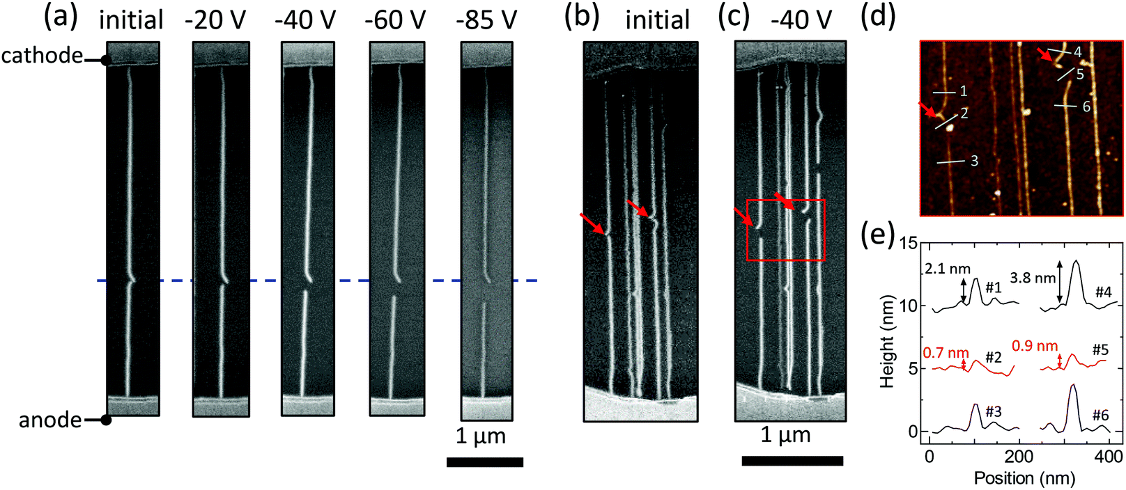 | ||
| Fig. 1 (a) SEM images of an SWNT after gap formation and gap extension in air. The initial gap was formed with a ramp voltage up to Vmax = 25 V on a heated substrate, followed by subsequent application of Vmax = 20, 40, 60 and 85 V at room temperature. SEM images of SWNTs (b) after nanogap formation and (c) after gap extension with ramp voltage up to Vmax = 40 V was applied. (d) AFM image of the region outlined in red in (c). The initial gap location is indicated by arrows. (e) Cross-sectional profiles of two sets of SWNTs (black) and gaps (red) at the positions numbered 1 to 6 in (d). | ||
Similar experiments in air were performed for SWNT arrays with channel lengths of Lch = 6.2 and 8.3 μm, by changing the maximum voltage from Vmax = 40 to 100 V with 20 V steps. Typically ten SWNTs were first broken down for the following gap extension experiment under each condition, while most s-SWNTs were preserved by gate control. Each maximum voltage was applied to different SWNT arrays for the same length of time, although the size of gaps extended with a constant voltage applied for 1 s did not further change even after 1000 s in a control experiment. The size of the extended SWNT gaps with Lch = 6.2 and 8.3 μm is plotted as a function of Vmax in Fig. 2. Error bars indicate the standard deviation of the extended gap size. Similar gap size and voltage-dependence were obtained for SWNT arrays of both lengths. The etching of SWNTs on the anode side is self-terminated in a very short time, as is clear from the time-independence of the gap size. Therefore the etching length is simply determined by voltage, rather than by the product of the etching rate and etching time (see Fig. S2a in the ESI†). We will later discuss in detail how and why the gap size is dependent on the applied voltage. Note that exceptionally large gaps were excluded from Fig. 2 because some SWNTs can be etched due to the presence of closely-placed SWNTs, as discussed later with respect to Fig. 4.
 | ||
| Fig. 2 Gap size as a function of maximum applied voltages under various gas conditions (in air, dry O2, and wet O2). Circles (black) and open squares (blue) indicate the size of SWNT gaps extended in air with Lch = 6.2 and 8.3 μm, respectively. Inversed triangles (green) represent the size of the gaps formed by electrical breakdown in dry oxygen. Red triangles correspond to identical gap arrays further extended in wet oxygen with the same maximum voltages. Lch = 5.1 μm. Solid lines represent the best-fit of the data for each condition with eqn (3). | ||
We propose a mechanism for the SWNT gap size obtained by electrical breakdown on substrates as follows. The gaps initially have a gap size of <10 nm immediately after breakdown, as such small gaps were obtained in a previous study,15 and these gaps are readily extended by continuous application of a voltage. Chain-reaction burning of SWNTs could be considered to result in large gap formation, as reported in our previous study on organic film-assisted burning of SWNTs.4 However, the oxygen-induced chain reaction is not expected as long as the SWNTs are directly exposed to dry air and are in contact with the substrates. This is because the collision frequency of oxygen molecules with SWNTs in air (ca. 109 s−1) is relatively small compared to the thermal relaxation time of SWNTs on substrates (<100 ps).21 If chain-reaction burning dominates the gap formation process, then heating of the substrates during electrical breakdown should lead to larger gap formation. However, the experimental results given in Fig. S1† indicate the opposite. Furthermore, the electrical breakdown of SWNTs on substrates did not indicate a clear dependence on the partial pressure of oxygen (Fig. S4 in the ESI†).
The dependence of the gap size on the applied voltage can explain the previous finding that electrical breakdown of longer SWNTs resulted in larger gap formation.11,15 We simply approximate that the extended gap size is proportional to the maximum voltage for small gaps (Lgap = k1Vmax, where k1 is a constant). The breakdown voltage, the voltage required to heat up the SWNTs to oxidation temperature (typically ca. 600 °C), is proportional to the SWNT length (VBD = k2Lch, where k2 was determined as 4.48 V μm−1 in the previous studies) for long SWNTs (Lch > 1 μm).22,23 If the voltage is ramped until an SWNT is broken, then the extended gap size will also be proportional to the SWNT length (Lgap = k1VBD = k1k2Lch). Therefore, the use of shorter SWNTs (small Lch) is preferable for smaller nanogap applications in energy-efficient and highly-integrated devices.
Effect of ambient water vapor on gap extension
The dependence of gap extension on the ambient gas conditions was examined. Fig. 2 (green inverted triangles) shows the size of gaps formed in SWNTs with Lch = 5.1 μm by electrical breakdown up to four different Vmax in dry oxygen gas flow. The gap size here also represents the extended gap size due to voltage application after cutting of the SWNTs, although gap formation and gap extension processes were not separated. The gaps formed in dry oxygen were smaller than those in ambient air (Fig. 2), which suggests that oxygen molecules are not critical for the SWNT gap extension phenomenon, and that some other gas(es) in air play a key role.With a focus on the water vapor in air, the gaps were further extended in wet oxygen with the same maximum voltages as those in dry oxygen. Fig. 2 (red triangles) shows that the extended gap size achieved in wet oxygen is much larger than that under other conditions with a lower relative humidity (RH) (wet oxygen ca. 100% RH, dry oxygen ca. 0% RH, and laboratory ambient air 30–60% RH). Gap extension experiments conducted in wet nitrogen (data not shown) revealed similar results to those in wet oxygen, which also excludes the importance of oxygen in the gap extension process. Higher humidity resulted in larger gap size, which indicates that water vapor plays a key role in the voltage-driven extension of SWNT gaps. Based on this knowledge, the smaller gap formation by breakdown in the Ar gas flow (Lgap = 30–100 nm) than in air (Lgap = 30–200 nm), as reported previously,11 can be explained by the low humidity in the Ar gas flow, rather than by low oxygen partial pressure. Therefore, to further decrease the SWNT gap size, electrical breakdown should be performed in high-pressure dry oxygen. This is not only because dry gas prevents gap extension, but also because high-pressure oxygen lowers the breakdown voltage of SWNTs (see Fig. S4 in the ESI†).
Field emission at SWNT nanogaps
The SWNT gap extension process involves charge transfer and an etching reaction; therefore, the current–voltage (I–V) characteristics during gap extension in air were carefully observed (see Fig. S3 in ESI†). Although no conductive materials should be left at the gaps after breakdown of all SWNTs, a small and unstable current was still observed through the SWNT gaps. Recently, field emission (Fowler–Nordheim tunneling) at SWNT gaps on substrates with Lgap = 23–125 nm were examined using an electrostatic force microscopy technique.24 For gaps of m-SWNTs with any gap size or s-SWNTs with Lgap > 60 nm, field emission was revealed to be the dominant charge transfer mechanism. Field emission during electrical breakdown has been briefly discussed in the literature; however, there has been no detailed investigation.25To elucidate the charge transfer mechanism at the SWNT gaps in the present work, the field emission properties at m-SWNT nanogaps were measured in a vacuum (ca. 0.02 Pa) to avoid damage to the anode SWNTs (gap extension). An experimental device was fabricated that contains a single SWNT, as shown in Fig. 3a and b. I–V characteristics were measured for SWNT gaps with Lgap values of ca. 80 and 300 nm (Lch = 8.2 and 14.1 μm, respectively), by ramping the bias voltage from 0 V, while the gate voltage was kept equal to the cathode voltage. Fig. 3c shows I–V characteristics for these gaps, where steep current increases in the sub-nanoampere range were observed at 35 V (line (a) in Fig. 3c) and 110 V (line (b) in Fig. 3c). The Fowler–Nordheim (FN) plots for the measurement (Fig. 3d) yield almost straight lines (solid lines show the best-fits). When we assume the electrons were emitted into vacuum from SWNTs with a work function of 4.8 eV,26 the field enhancement factors γ for the gaps shown in Fig. 3a and b are calculated from the slopes27 to be 460 and 273, respectively. Note that γ = F/E, where F and E are a local field at the emitter surface and the macroscopic field (applied voltage V divided by the inter-electrode distance Lch), respectively. Despite the large difference in sample configuration, the field enhancement factors roughly correspond to a previous report for free-standing SWNT field emitters (γ = 515).27
 | ||
| Fig. 3 (a, b) SEM images of single SWNT gaps with Lgap = 80 and 300 nm, respectively. Insets show the enlarged images of the gaps. (c) I–V characteristics under vacuum and (d) FN plots of the SWNT gaps shown in (a, b). Red solid and blue dashed lines represent the fitted field emission properties with the data for the 80 nm gap and the field emission properties expected from geometrical features of the 300 nm gap, respectively. (e) I–V characteristics of three SWNT gaps formed with voltage application up to Vmax = 20 V. Inset: The current at 20 V (= Vmax) is estimated by extrapolation of the FN plot. | ||
The field emission characteristics for three similar SWNT gaps were also compared. Following gap formation by electrical breakdown on heated substrates (ca. 100 °C), the gaps were extended with Vmax = 20 V in air at room temperature. The size of all the extended gaps was around 70 nm. As shown in Fig. 3e, the I–V characteristics of these gaps in a vacuum show onset voltages around 25–35 V, which were slightly larger than the maximum voltage (Vmax = 20 V) for gap extension. These gaps were extended with Vmax = 20 V; therefore, the minimum current required for in-air gap extension (threshold current) can be estimated from the emission current at V = 20 V in a vacuum. The extrapolation of the FN plot for the gap drawn in blue yielded a threshold current of 0.1–1 fA at V = 20 V (inset of Fig. 3e, see also Fig. S7 in the ESI†), which was beyond the range of measurement due to noise in the present setup. It should be noted, however, that the field emission properties of SWNTs can be affected by the adsorption of oxygen and water molecules in air.28,29 Note that the linear current component obtained from the device without SWNTs (I/V = 14.9 [fA V−1]) was deducted in Fig. 3e to exclude leakages that did not originate from the SWNTs.
Although the field emission current was measured in a vacuum, the surface leakage current via water adsorbed on the substrates must be considered as another conduction mechanism in the presence of water vapor. Charge transfer between SWNTs and water electrolyte (electrochemical reaction) requires an electric field with a specific strength at the interface. Therefore, a higher voltage is required to maintain the constant field strength for larger SWNT gaps, which may appear as the observed relationship between the applied voltage and gap size (Fig. 2). Even in that case, the field emission measurement in a vacuum is useful for quantification of the field enhancement at SWNT tips.
Threshold field for gap extension: voltage vs. gap size
Now the validity of the field emission electron as a cause of SWNT etching is evaluated. We suppose that the emission current is kept constant (threshold current, I0) during the gap extension process because the gap size changes according to the ramp voltage. The FN law gives the relation between the emission current I [A], and the local field at the emitter surface F [V m−1], as:30 | (1) |
 .32 For the case of smaller D, γ = γ0 × {1 + a × [D/(D + h)]−1 − b × [D/(D + h)]} is often used as the modified relation,27 where a and b are constants. The relation can be further rewritten to match the configuration of the present samples (see S5 in the ESI† for details):
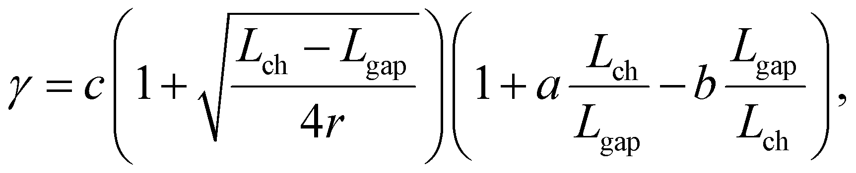 | (2) |
 | (3) |
Eqn (3) was fitted to the experimental data in Fig. 2 with a and F0/c as fitting parameters. The diameter of all the SWNTs was assumed to be 1.5 nm.33 When a = 0.11, the fitting lines corresponded well with the trend of the experimental data under all the conditions, as shown in Fig. 2 (see Fig. S6a in the ESI† for different a values). The b constant has little effect on the fitting results; therefore, b was set at zero. Compared to the threshold field F0,air obtained from the data in air (Lch = 6.2 μm), the other threshold field strengths for the gap extension in wet oxygen (Lch = 5.1 μm), in air (Lch = 8.3 μm), and in dry oxygen (Lch = 5.1 μm) were 0.47F0,air, 1.04F0,air, and 1.80F0,air, respectively. Enhancement of the emission current at a given field by water adsorption on SWNTs29,34 can account for the lower threshold field under higher humidity conditions. Switching of the major charge transfer mechanisms from field emission to the surface leakage current is another possible explanation for the low threshold field in wet oxygen.
This relationship was further applied to the calculation of the I–V characteristics for field emission using the FN law (eqn (1)). Now, for simplicity, an SWNT diameter dt of 1.5 nm and ϕ = 4.8 eV are supposed. The emission area A is estimated from the y-intercept of the FN plot to be 7.0 × 10⁻¹² m2. First, c = 0.66 was obtained by fitting with the field emission characteristics of the 80 nm gap shown in Fig. 3c (red line). The I–V characteristics for the 300 nm gap were then predicted from the gap configuration using eqn (1) and (2). As shown in Fig. 3c, the predicted I–V characteristics (blue dashed line) are in good accordance with the experimental results (see Fig. S6b in the ESI† for different a values). This indicates that the relationship between the geometric features and the field enhancement factor γ (eqn (2)) is useful to predict the field emission characteristics of SWNT gaps on substrates, and also that the gap extension is dominated by the geometrically-derived field enhancement at the SWNT tips. Note that the Lch values of 12.5 and 11.5 μm were substituted into eqn (2) for 80 and 300 nm gaps, respectively, because the length of the SWNTs on the cathode side rather than the distance between two metal (Pd) contacts influences the field enhancement (see Fig. S6 in the ESI†). The threshold field strength in air F0,air = 1.7 × 10⁹ V m−1 was obtained from the threshold current I0 = 0.1–1 fA. Field emission into a vacuum was assumed here, although a similar comparison of the 80 nm and 300 nm gaps is possible for field emission (FN tunneling) into SiO2 with slight modification of the parameters.
Taking field-emission electrons and water molecules into account, we propose two mechanisms for SWNT etching as follows. Under ambient air, the SWNT surface is covered with a few layers of water molecules35,36 The first possible mechanism is the electrochemical etching of anode SWNTs,37 where charge transfer occurs via field emission or a water-mediated surface current. Electrochemical oxidation first occurs on the SWNT surfaces, which forms covalently functionalized groups. The locally functionalized SWNTs are then removed through further oxidation. The total reaction can be expressed as C(SWNT) + 3OH− → CO32− + 3H+ + 4e−. In contrast to the electrochemical etching of SWNTs in bulk electrolytes, physisorbed water from the air is unlikely to form an electric double layer under the conditions of the present experiments, which typically strengthens the field at the SWNT–electrolyte interfaces. Instead, field enhancement at the SWNT tips due to the ultrahigh aspect ratio may play an important role in the oxidation process. SWNT etching may continue either until the gaps are extended to a sufficient extent for the emission current to be negligible or until the local field at the tips become weak enough not to cause the electrochemical reaction.
A second possible explanation for the gap extension is as follows. Electrons emitted from the cathode tips are accelerated by an electric field while flowing between the SWNT gaps. Physisorbed water molecules on the SWNT tips are ionized by accelerated electrons and turn into highly reactive species, such as OH˙, H˙, and  radicals. These species then etch neighboring carbon atoms of the SWNTs to form CO, CO2, and various hydrocarbons. A similar etching phenomenon was reported in studies on CNT cutting6 and the machining of CNT forests,38 where CNTs were cut with a low-energy focused electron beam (with SEM) in the presence of water vapor inside the chamber.
Electrical breakdown on heated substrates resulted in smaller gap formation because the water molecules on the SWNT surfaces desorb at high temperature, even under the same water vapor pressure (see Fig. S1 in ESI†). This indicates the importance of adsorbed water molecules rather than water molecules in the gas phase, which supports both the mechanisms proposed here. Even when the emission current is sufficiently large, the gaps are not extended in the absence of water molecules on anode side SWNTs (e.g., in a vacuum).
Remote etching among adjacent SWNTs
We also identified the remote etching phenomenon of anode SWNTs parallel to cathode SWNTs with small inter-SWNT spacing, as shown in Fig. 4a. Here, the SWNTs that connect only with metal anodes or cathodes are referred to as A-SWNTs or C-SWNTs, respectively. Gaps were first formed at a red arrow position and then extended to an Lgap of a few microns, whereas the other two gaps were only extended to an Lgap of a few hundreds nanometers. This can be explained by field enhancement between the side walls of A- and C-SWNTs,39 which induces the etching of adjacent A-SWNTs, as schematically shown in Fig. 4b. Red and blue colors in the schematic illustration indicate high and low electric potential, respectively. A-SWNTs (red) within a certain distance from C-SWNTs (inside the gray region) are etched away. Although this etching mechanism is intrinsically the same as gap extension, the extent to which the SWNTs are etched away is determined by the distance between the two gaps of A- and C-SWNTs. In addition, the occurrence of etching is dependent on the inter-SWNT spacing of two parallel SWNTs and the applied voltage. If uniformly dense SWNT arrays can be grown and also m- and s-SWNTs are intentionally cut near cathodes and anodes, respectively, then this parallel etching could be used to eliminate only m-SWNTs by utilizing selective field emission from the side walls of s-SWNTs (see Fig. S8 in the ESI† for details of the possible process).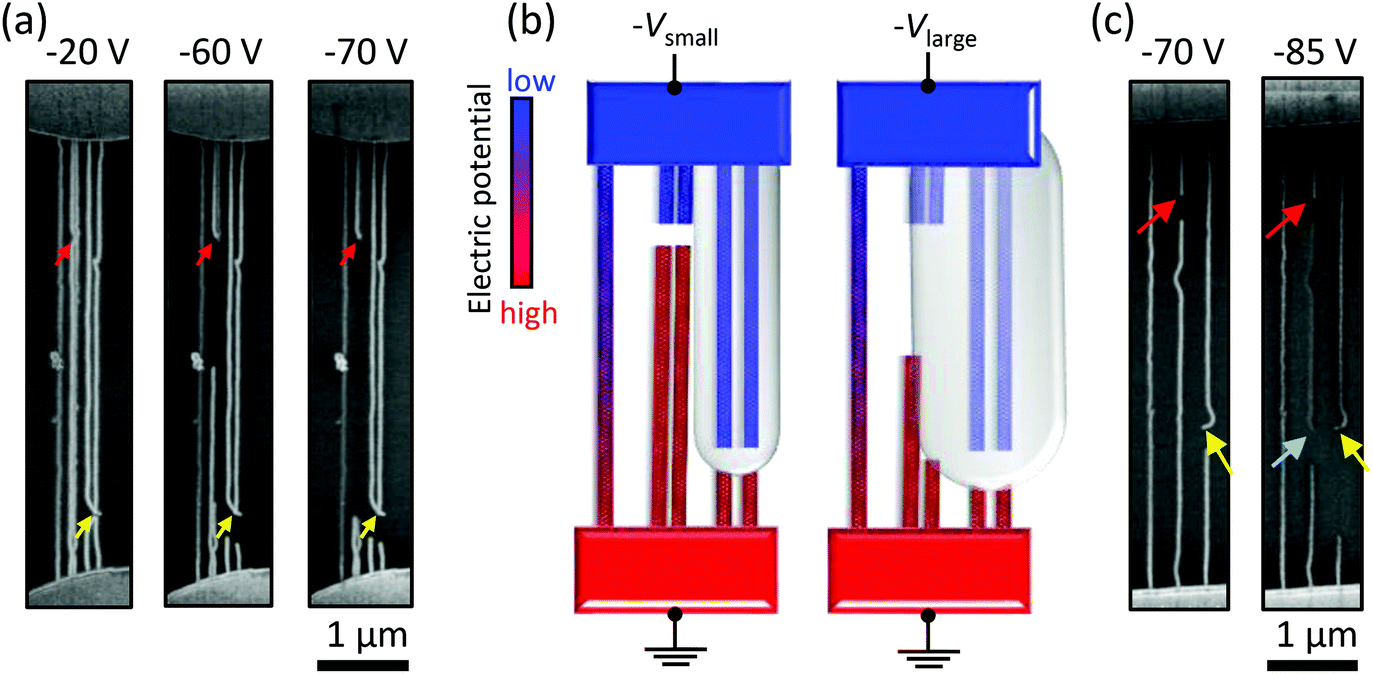 | ||
| Fig. 4 (a) SEM images of five parallel SWNTs. Each image was taken after voltage application up to Vmax as indicated. The red and yellow arrows indicate the initial gap location on the anode and cathode SWNTs (A- and C-SWNTs), respectively. Two A-SWNTs in the middle were etched from over a few microns because of right C-SWNTs. (b) Schematic illustrations of the electric potential at two stages of the SWNT array in (a). Left: After the gap formation at the red arrow position, corresponding to 20 V < Vmax < 60 V. Right: After the remote etching of A-SWNTs, corresponding to Vmax = 60 V. Field emission from C-SWNTs can affect A-SWNTs inside the gray area. (c) SEM images for the double cutting of a single SWNT. Secondary cutting of the middle SWNT occurred at the position marked by the blue arrow. | ||
This type of etching may deteriorate the removal selectivity during electrical breakdown by cutting or damaging the adjacent s-SWNTs. For example, the SWNT that did not bridge two metallic contacts due to electrical breakdown was cut again around the neighboring nanogap, as indicated by a blue arrow in Fig. 4c (also see Fig. S3†). This indicates that SWNTs can be broken down without Joule self-heating if nanogaps are present in the vicinity. The SWNT segment between the red and blue arrows had a low contrast to the substrate in the SEM image, which also indicates the physical isolation of the SWNT segment from other SWNTs and metal electrodes.40
If ionization of water by accelerated electrons induces the cutting of unbridged SWNTs, then operation with voltages smaller than the ionization energy of water (ca. 12.7 eV) would be helpful to avoid deterioration of the removal selectivity. The electrical breakdown of SWNT arrays (ca. 20 SWNTs μm−1, Lch = 2 μm), where a bias voltage of up to 20 V was applied, resulted in the correlated breakdown of neighboring SWNTs,19 though this was previously explained in a different way.20 In contrast, the electrical breakdown of a higher density but shorter SWNT arrays (>100 SWNTs μm−1, Lch = 400 nm), where the breakdown voltage is always <8 V, successfully cut only m-SWNTs (current retention >20%).41 Note that a relatively thick gate dielectric (Al2Ox, 25 nm equivalent oxide thickness) compared to the inter-SWNT spacing (<10 nm) was used, and a high electric field (>10 V μm−1) was applied.41 The results of adjacent SWNT etching will thus provide a guide to the design of appropriate device structures and the experimental conditions required for successful SWNT purification.
Conclusions
We have reported on the field emission and voltage-driven gap extension phenomena for SWNTs on substrates. The gap extension clearly showed one-directionality and dependence on the applied voltage and humidity. Therefore, the SWNT gap size can be controlled by changing the water vapor pressure, substrate temperature, and voltage. Size controllability will broaden the application of nanogaps, especially as nanoscale electrodes. The I–V characteristics of single gap devices under vacuum indicated FN tunneling features, which corresponds well with the characteristics predicted from the FN law and the field enhancement model that was calibrated using the gap extension results. Electrochemical oxidation and charge transfer via field emission are thus possible driving forces of SWNT gap extension. In addition, unintentional damage to the neighboring SWNTs induced by field enhancement between adjacent SWNTs should be minimalized when electrical breakdown is employed to selectively cut m-SWNTs for semiconductor applications.Experimental
SWNT growth and device fabrication
Metal electrodes (Ti/Pd or Ti/Au; 5/20 nm) were photolithographically patterned using sputtering on a highly p-doped Si substrate with a 100 nm thick thermal oxide layer. Horizontally aligned SWNTs were grown by the alcohol catalytic chemical vapor deposition method33,42 on r-cut crystal quartz substrates, and then transferred onto the Si/SiO2 substrates with patterned electrodes via poly(methyl methacrylate) (PMMA) thin films.43 Unwanted SWNTs outside channel regions were etched by oxygen plasma to isolate the devices. Each device has 20 μm wide electrodes with 5–15 μm spacing and typically contains 30 SWNTs (density of 1.5 SWNTs μm−1), which is suitable to avoid interaction and bundling among adjacent SWNTs.SWNT nanogap preparation
SWNT nanogaps were prepared using the electrical breakdown technique. Electrical breakdown was first performed on a hotplate (ca. 100 °C) because the breakdown of SWNTs on heated substrates was found to result in smaller gap formation than that at room temperature, as shown in Fig. S1 of the ESI.† The gap location was checked by scanning electron microscopy (SEM; 1 kV, S-4800, Hitachi Co., Ltd) or atomic force microscopy (AFM; SPI3800N, SII).Nanogap extension
A ramp voltage was applied from 0 to negative maximum voltage (−Vmax) to the nanogaps for a typical period of 100 s at room temperature, and the extent of gap extension was observed. The gap extension experiments were conducted under various gas conditions, such as in air, and in dry or wet oxygen gas flow. Dry oxygen was obtained directly from an oxygen gas cylinder and was flowed onto the substrates. Wet oxygen was obtained using the water bubbler technique (see the setup used in Fig. S2b of the ESI†) at room temperature to provide saturated water vapor (ca. 3 kPa). A voltage was also applied to SWNT gaps under vacuum (ca. 0.02 Pa) to avoid gap extension and observe the I–V characteristics at gaps of a certain size.Acknowledgements
A part of this work was financially supported by Grants-in-Aid for Scientific Research (No. 15H05760, 25107002, 26420135) and the IRENA Project of JST-EC DG RTD, Strategic International Collaborative Research Program (SICORP). This work was partly conducted at the Center for Nano Lithography & Analysis, and VLSI Design and Education Center (VDEC), the University of Tokyo. K. O. was financially supported by a Japan Society for the Promotion of Science (JSPS) Fellowship (15J07857).References
- P. G. Collins, M. S. Arnold and P. Avouris, Science, 2001, 292, 706–709 CrossRef CAS PubMed.
- N. Patil, A. Lin, J. Zhang, H. Wei, K. Anderson, H.-S. P. Wong and S. Mitra, IEEE Trans. Nanotechnol., 2011, 10, 744–750 CrossRef.
- M. M. Shulaker, G. Hills, J. Payne, H. Wei, H.-Y. Chen, H.-S. P. Wong and S. Mitra, Nature, 2013, 501, 526–530 CrossRef CAS PubMed.
- K. Otsuka, T. Inoue, S. Chiashi and S. Maruyama, Nanoscale, 2014, 6, 8831–8835 RSC.
- J. Li, A. D. Franklin and J. Liu, Nano Lett., 2015, 15, 6058–6065 CrossRef CAS PubMed.
- T. D. Yuzvinsky, A. M. Fennimore, W. Mickelson, C. Esquivias and A. Zettl, Appl. Phys. Lett., 2005, 86, 053109 CrossRef.
- C. Thiele, M. Engel, F. Hennrich, M. M. Kappes, K.-P. Johnsen, C. G. Frase, H. V. Löhneysen and R. Krupke, Appl. Phys. Lett., 2011, 99, 173105 CrossRef.
- A. Cui, H. Dong and W. Hu, Small, 2015, 11, 6115–6141 CrossRef CAS PubMed.
- X. Guo, J. P. Small, J. E. Klare, Y. Wang, M. S. Purewal, I. W. Tam, B. H. Hong, R. Caldwell, L. Huang, S. O'brien, J. Yan, R. Breslow, S. J. Wind, J. Hone, P. Kim and C. Nuckolls, Science, 2006, 311, 356–359 CrossRef CAS PubMed.
- C. W. Marquardt, S. Grunder, A. Błaszczyk, S. Dehm, F. Hennrich, H. V. Löhneysen, M. Mayor and R. Krupke, Nat. Nanotechnol., 2010, 5, 863–867 CrossRef CAS PubMed.
- F. Xiong, A. D. Liao, D. Estrada and E. Pop, Science, 2011, 332, 568–570 CrossRef CAS PubMed.
- P. Collins, M. C. Hersam, M. Arnold, R. Martel and P. Avouris, Phys. Rev. Lett., 2001, 86, 3128–3131 CrossRef CAS PubMed.
- A. D. Liao, R. Alizadegan, Z.-Y. Ong, S. Dutta, F. Xiong, K. J. Hsia and E. Pop, Phys. Rev. B: Condens. Matter, 2010, 82, 205406 CrossRef.
- E. Pop, D. A. Mann, Q. Wang, K. E. Goodson and H. Dai, Nano Lett., 2006, 6, 96–100 CrossRef CAS PubMed.
- P. Qi, A. Javey, M. Rolandi, Q. Wang, E. Yenilmez and H. Dai, J. Am. Chem. Soc., 2004, 126, 11774–11775 CrossRef CAS PubMed.
- J. Y. Huang, S. Chen, S. H. Jo, Z. Wang, D. X. Han, G. Chen, M. S. Dresselhaus and Z. F. Ren, Phys. Rev. Lett., 2005, 94, 236802 CrossRef CAS PubMed.
- K. Mølhave, S. B. Gudnason, A. T. Pedersen, C. H. Clausen, A. Horsewell and P. Bøggild, Nano Lett., 2006, 6, 1663–1668 CrossRef PubMed.
- T. Kim, T. J. Kang, K. Li, E. Y. Jang, J. S. Lee, D. K. Seo, H. Im and Y. H. Kim, Sens. Actuators, B, 2012, 173, 517–522 CrossRef CAS.
- S. Shekhar, M. Erementchouk, M. N. Leuenberger and S. I. Khondaker, Appl. Phys. Lett., 2011, 98, 243121 CrossRef.
- M. A. Wahab and M. A. Alam, IEEE Trans. Electron Devices, 2014, 61, 4273–4281 CrossRef CAS.
- Z.-Y. Ong and E. Pop, Phys. Rev. B: Condens. Matter, 2010, 81, 155408 CrossRef.
- E. Pop, Nanotechnology, 2008, 19, 295202 CrossRef PubMed.
- E. Pop, D. A. Mann, K. E. Goodson and H. Dai, J. Appl. Phys., 2007, 101, 093710 CrossRef.
- K. A. S. Araujo, A. P. M. Barboza, T. F. D. Fernandes, N. Shadmi, E. Joselevich, M. S. C. Mazzoni and B. R. A. Neves, Nanoscale, 2015, 7, 16175–16181 RSC.
- A. Javey, J. Guo, M. Paulsson, Q. Wang, D. Mann, M. Lundstrom and H. Dai, Phys. Rev. Lett., 2004, 92, 106804 CrossRef PubMed.
- S. Suzuki, C. Bower, Y. Watanabe and O. Zhou, Appl. Phys. Lett., 2000, 76, 4007 CrossRef CAS.
- J.-M. Bonard, K. Dean, B. Coll and C. Klinke, Phys. Rev. Lett., 2002, 89, 197602 CrossRef PubMed.
- A. Wadhawan, R. E. Stallcup, K. F. Stephens, J. M. Perez and I. A. Akwani, Appl. Phys. Lett., 2001, 79, 1867 CrossRef CAS.
- K. A. Dean, P. von Allmen and B. R. Chalamala, J. Vac. Sci. Technol., B: Microelectron. Nanometer Struct.–Process., Meas., Phenom., 1999, 17, 1959 CrossRef CAS.
- I. Brodie and C. A. Spindt, Adv. Electron. Electron Phys., 1992, 7, 1–106 Search PubMed.
- C. J. Edgcombe and U. Valdrè, J. Microsc., 2001, 203, 188–194 CrossRef CAS.
- R. C. Smith, D. C. Cox and S. R. P. Silva, Appl. Phys. Lett., 2005, 87, 103112 CrossRef.
- T. Inoue, D. Hasegawa, S. Badar, S. Aikawa, S. Chiashi and S. Maruyama, J. Phys. Chem. C, 2013, 117, 11804–11810 CAS.
- A. Maiti, J. Andzelm, N. Tanpipat and P. von Allmen, Phys. Rev. Lett., 2001, 87, 155502 CrossRef CAS PubMed.
- Y. Homma, S. Chiashi, T. Yamamoto, K. Kono, D. Matsumoto, J. Shitaba and S. Sato, Phys. Rev. Lett., 2013, 110, 157402 CrossRef PubMed.
- S. Chiashi, K. Kono, D. Matsumoto, J. Shitaba, N. Homma, A. Beniya, T. Yamamoto and Y. Homma, Phys. Rev. B: Condens. Matter, 2015, 91, 155415 CrossRef.
- D. Wei, Y. Liu, L. Cao, H. Zhang, L. Huang, G. Yu, H. Kajiura and Y. Li, Adv. Funct. Mater., 2009, 19, 3618–3624 CrossRef CAS.
- B. Rajabifar, S. Kim, K. Slinker, G. J. Ehlert, A. J. Hart and M. R. Maschmann, Appl. Phys. Lett., 2015, 107, 143102 CrossRef.
- Y. Shiratori, K. Furuichi, S. Noda, H. Sugime, Y. Tsuji, Z. Zhang, S. Maruyama and Y. Yamaguchi, Jpn. J. Appl. Phys., 2008, 47, 4780–4787 CrossRef CAS.
- R. Y. Zhang, Y. Wei, L. A. Nagahara, I. Amlani and R. K. Tsui, Nanotechnology, 2006, 17, 272–276 CrossRef CAS.
- M. M. Shulaker, G. Pitner, G. Hills, M. Giachino, H.-S. P. Wong and S. Mitra, in 2014 IEEE International Electron Devices Meeting, 2014, vol. 4, pp. 33.6.1–33.6.4.
- S. Maruyama, R. Kojima, Y. Miyauchi, S. Chiashi and M. Kohno, Chem. Phys. Lett., 2002, 360, 229–234 CrossRef CAS.
- L. Jiao, B. Fan, X. Xian, Z. Wu, J. Zhang and Z. Liu, J. Am. Chem. Soc., 2008, 130, 12612–12613 CrossRef CAS PubMed.
Footnote |
| † Electronic supplementary information (ESI) available. See DOI: 10.1039/c6nr05449h |
| This journal is © The Royal Society of Chemistry 2016 |