
Development of a high performance high voltage insulator for power transmission lines from blends of polydimethylsiloxane/ethylene vinyl acetate containing nanosilica†
Dipankar Ghosh,
Subhendu Bhandari,
Tapan Kumar Chaki and
Dipak Khastgir*
Rubber Technology Centre, Indian Institute of Technology Kharagpur, Kharagpur-721302, West Bengal, India. E-mail: khasdi@rtc.iitkgp.ernet.in; Tel: +91-3222-283192
First published on 17th June 2015
Abstract
Ceramic materials are commonly used as outdoor insulators for high voltage power transmission lines. Presently these ceramic insulators are replaced by composite polymeric insulators with silicone rubber (PDMS) housing, especially in industrial areas with pollution. Silicone rubber is chosen for housing material because of its excellent aging resistance, electrical properties, tracking resistance, and stable hydrophobicity which in turn control the tracking resistance. However, the material has deficiencies like poor mechanical strength and high cost. To improve the mechanical properties and reduce the cost, silicone rubber is blended with ethylene vinyl acetate copolymer (EVA). The optimum blend composition is found to be PDMS/EVA 60/40 w/w. But in doing so some reduction in hydrophobicity is observed, thus adversely affecting the tracking resistance. To improve hydrophobicity, the addition of nanosilica at the level of 6 phr is found to be the optimum. Thus high performance outdoor insulators can be produced from a PDMS–EVA blend containing 6 phr nanosilica. Different types of accelerated aging tests were performed on the insulator samples to simulate their aging behavior under different real life aging processes.
1. Introduction
Electrical insulators are one of the most important elements in power transmission systems. Weaknesses/flaws in the insulator may cause system failure leading to an interruption in power supply. Conventional ceramic insulators are nowadays getting replaced by polymeric composite insulators.1,2 Nonceramic composite insulators consist of two components, i.e., the core made of a composite of fiberglass with polyester or epoxy,3,4 and the housing, made of insulating polymers like silicone rubber (PDMS),5,6 ethylene vinyl acetate copolymer (EVA),7 and ethylene propylene diene rubber (EPDM) etc.8,9 The main advantages of polymeric insulators over conventional ceramic insulators are their lighter weight, ease of transportation (unbreakable) and installation in the electrical transmission lines.10 Silicone elastomer (PDMS) is the most preferred material for the outer housing of composite insulators because of its better hydrophobicity11 and reduced tendency to cause electrical flashover due to low leakage current possibilities.12 PDMS does not get much affected by contaminants due to the migration of low molecular weight fragments from the bulk to the surface which makes the surface hydrophobic and also encapsulates the contaminant, maintaining the hydrophobic character of the surface to a great extent.13–15 This migration process is a continuous one, as a result, the hydrophobicity of the surface is maintained to the level required for preventing surface tracking (surface electrical flashover).16 The detrimental environmental effects on insulators due to the exposure in open atmosphere which includes UV rays and heat from the sun, rain and moisture from dew.17–20 The loss of the low molecular weight fractions of PDMS from the surface is due to accelerated aging such as treatment with boiling water, and exposure to heat or UV, causes a reduction in the low molecular weight fractions of PDMS on the surface. This process of loss and regain of the low molecular weight fractions due to the migration from the bulk to the surface to retain the surface characteristics is not a perpetual process and cannot continue lifelong. With increased aging time, the migration of the low molecular weight fractions from the bulk reduces and then regains surface hydrophobicity, and is adversely affected thereby causing surface failure due to electrical tracking.21–23 The surface of an outdoor insulator should be hydrophobic in nature so that discrete water droplets formed by rain and/or dew on the insulator surface should not coalesce to form continuous channels causing surface tracking under high voltage application. How the environmental conditions adversely affect the surface characteristics of a polymeric high voltage insulator are schematically represented with a figure in the graphical abstract.Materials with a contact angle against water of greater than 90° are considered to be hydrophobic in nature, whereas materials having a contact angle of less than 90° are considered to be hydrophilic.24 The copolymer EVA (28% VA content), having contact angle ∼92° exists more or less on the border line,25 whereas PDMS has a contact angle of ∼113° and is considered to be a very good hydrophobic material26 with better ability to reduce the leakage current and consequently less chance of electrical discharge at the insulator surface.12,27
Commercially available cheaper EVA (28% VA) has much better mechanical properties than PDMS. The blending of the EVA with PDMS is expected to improve the mechanical properties28 while retaining the insulating characteristics of the PDMS to a great extent. In reality, the blending of these two polymers will compensate an individual’s property-deficiencies and will provide a cost effective material for high voltage insulator application. However, the properties of an insulator housing material not only depend on the base polymer/polymer blends, but also on the type, amount, shape and size of the filler incorporated in the matrix polymer.6,29
Alumina trihydrate (ATH) is used as a primary filler in large quantities in the insulator and it contributes to better erosion and tracking resistance.30,31 Some literatures reveal the use of hydrophobic nanosilica as a secondary filler in a polymer matrix to improve hydrophobicity.32–37
In the present work, an effort has been made to develop a high performance insulator housing compound by partial replacement of the PDMS with EVA to improve the mechanical properties and cost effectiveness. The optimization of the blend composition has been done and deficiencies encountered in the blend compared to a neat PDMS based insulator composite have been compensated through the addition of nanosilica. The loading of the nanosilica has also been optimized in the insulator composition. The optimized blend composite was exposed to different accelerated aging conditions to assess the service performance of these insulators.
2. Experimental
2.1 Materials
2.2 Sample preparation and identification
The preparation of the different blends of silicone rubber and EVA was accomplished in a Brabender Plasti-Corder, PLE-330 at the temperature 120 °C with a rotor speed of 60 rpm. To evaluate the effect of the addition of the nanosilica on different properties, a series of test samples were prepared. The nanofiller concentration was varied but was restricted up to the maximum level of 12 parts per hundred parts of rubber (phr) for the investigation. At the first stage of mixing, the EVA was added in the mixer and was allowed to melt for 2 min, followed by the addition of the PDMS (silicone rubber) and the mixing was continued for up to 4 minutes thereafter the addition of the filler, plasticizer (silicone oil + paraffinic oil), and antioxidant were done. Another 4 minutes was allowed for the proper mixing of all the added ingredients and the final addition of the curative was done and mixing was continued for 1 more minute. Then the whole mass was taken out from the Brabender and was passed through the open mixing mill for final sheeting. Different samples were sheeted out from the mill and were subjected to curing for the optimum cure time at 165 °C as evaluated from Monsanto Rheometer.2.3 Different modes of aging
Cured samples of all the compositions were subjected to different accelerated aging tests through exposing them to boiling water, high temperature (150 °C) and UV light by artificial accelerated aging. The aging process under boiling water and high temperature (dry heat in an aging oven) were continued for up to 7 days. However, UV aging was carried out for a maximum of up to 2 h. An UV chamber with high power UV light obtained from Western Quartz, USA (1800 watt quartz lamp, wavelength 250–350 nm) was used (ACS 21-22, cabinet built by Advance Curing System, Bangalore, India). The distance between the sample and the UV source was kept fixed at 7 cm. All the samples were naturalized for 24 h after aging prior to taking measurements of the different properties for these aged samples.2.4 Characterizations
The different mechanical properties were measured using a Hansfield Universal testing machine (H10KS) as per the ASTM D 412-98. The volume and surface resistivities of different samples were measured using an Agilent High Resistance Meter (4339B) coupled with an Agilent Resistivity Cell (16008B). Dielectric properties (dielectric constant and dielectric loss) were measured using a Novocontrol Alpha-A Analyzer, Novocontrol Technologies, Germany. The static contact angle was measured using a CA Goniometer (Rame-Hart Instrument Co, 264 F4). The hardness was measured using a Durometer type A (Shore Instruments and MFG Co, INC, USA, CV-71200, CONVELOADER). Electrical tracking analysis was done using a Siemens and Halske Aktiengesellschaft instrument, Germany. The surface morphologies of the different samples were analyzed using FESEM, field emission scanning electron microscopy (SUPRA 40, ZEISS, Germany), AFM, atomic force microscopy (tapping mode, Agilent Technologies, 5500) and TEM, transmission electron microscopy (SUPRA 40, Karl ZEISS, Germany).3. Results and discussion
3.1 Optimization of PDMS/EVA blend composition
Stress–strain plots of the different PDMS/EVA blends and the optimized blend with different nanosilica loadings are presented in Fig. 1a and b respectively. Fig. 1a exhibits the increase in tensile strength and the elongation at the break with the increase in the proportion of EVA in the blends. This can be attributed to the strain induced crystallization of EVA which is semicrystalline in nature and acts as a stronger component in the blend. That is why the PDMS rich blends are comparatively weaker whereas the EVA rich blends are stronger with a higher elongation at the break. The blend composition containing 60 wt% of PDMS shows an adequate strength of about 3.6 MPa with an elongation at the break of 275%, and is quite suitable for application in high voltage insulators. The surface resistivity is considered as one of the important characteristics of a high voltage insulator. The surface resistivity increases with the increase in PDMS concentration in the blend (Fig. 2a). However, the decrease in the surface resistivity is relatively less for the blend compositions diluted with EVA up to 40 wt%, beyond which a sharp fall in the resistivity is observed. The resistivity of the PDMS rich blend is mainly governed by the resistivity of the continuous PDMS matrix rather than the dispersed EVA phase.38 Again, the increase of the contact angles with the increase in PDMS concentration in the blends implies more of a hydrophobic nature of the insulation surface as required for the non-wettability characteristics of an insulation surface (Fig. 2b). A blend with a higher EVA content exhibits a reduction in the contact angle due to the presence of the polar vinyl acetate group. In real life the insulator is exposed to an open atmosphere, resulting in the reduction of surface hydrophobicity. This leads to the easy formation of water streams or water lines from the isolated water droplets generated from dew. These water lines cause electrical discharge on an insulator surface under high voltage. Thus the suitable material for a high voltage insulator should have enough mechanical strength, high surface resistivity, and good hydrophobicity along with an attractive price. | ||
Fig. 1 Stress–strain plot of (a) PDMS/EVA blends with different PDMS![[thin space (1/6-em)]](https://www.rsc.org/images/entities/char_2009.gif) :EVA ratio, (b) PDMS/EVA composites with different concentrations of nanosilica. :EVA ratio, (b) PDMS/EVA composites with different concentrations of nanosilica. | ||
 | ||
| Fig. 2 Change in (a) surface resistivity and (b) contact angle of PDMS/EVA blends with different PDMS:EVA ratios. | ||
3.2 Optimization of nanofiller concentration in the optimized blend composition
| Sample designation | Sample composition | |||||
|---|---|---|---|---|---|---|
| PDMS (phr) | EVA (phr) | ATH (phr) | Silicone oil (phr) | Paraffinic oil (phr) | Nanosilica (phr) | |
| PES0 | 60 | 40 | 100 | 10 | 5 | 0 |
| PES3 | 60 | 40 | 100 | 10 | 5 | 3 (0.74 vol%) |
| PES6 | 60 | 40 | 100 | 10 | 5 | 6 (1.48 vol%) |
| PES9 | 60 | 40 | 100 | 10 | 5 | 9 (2.20 vol%) |
| PES12 | 60 | 40 | 100 | 10 | 5 | 12 (2.92 vol%) |
FESEM of the optimized PDMS/EVA blend with the different loadings of nanosilica are presented in Fig. 3a–f. It can be seen that for up to 6 phr, the nanosilica filled composites show a relatively smooth surface morphology. However, for the systems with filler loadings beyond 6 phr, the increased surface roughness is apparent from the FESEM pictures. This is mainly because of the improper dispersion of the nanosilica particles at high loading (>6 phr) due to the formation of strong aggregates. The matrix polymer contains silicon as an element in the backbone, the filler also contains silicon. The existence of nanosilica on the composite surface can be confirmed by EDX analysis.
 | ||
| Fig. 3 FESEM micrograph of (a) nanosilica, (b) 0, (c) 3, (d) 6, (e) 9 and (f) 12 phr nanosilica filled nanocomposites. | ||
The variation in the atomic% concentration of elemental silicon (Si) with respect to elemental carbon (C) as measured from EDX (Fig. 4) confirms the increase in the silica concentration on the sample surface almost linearly with the increase in the nanosilica concentration.
 | ||
| Fig. 4 Atomic% of Si:C with the increasing of nanofiller concentration. | ||
 | ||
| Fig. 5 Variation of (a) dielectric constant (ε′) and (b) dielectric loss (ε′′) against the applied frequency with varying nanosilica content. | ||
The surface resistivity increases from 8.5 × 10¹⁴ for the unfilled blend (PES0) to 2.5 × 10¹⁵ ohm cm for the 6 phr filled blend (PES6). The surface resistivity of the 12 phr filled sample (PES12) however reduces to 1.5 × 10¹⁵ ohm cm which is comparable to that of the 3 phr loaded sample PES3 (1.6 × 10¹⁵) ohm cm (Fig. 6a).
 | ||
| Fig. 6 Change of (a) surface resistivity and (b) contact angle with the variation of nanosilica concentration. | ||
Considering both the bulk and the surface electrical properties, it may be concluded that the nanosilica can be dispersed with better homogeneity up to 6 phr loading, beyond which the filler particles get clustered and non-uniformly distributed as is evident from the FESEM analysis (Fig. 3 and S1†). The surface resistivity increases with nanosilica loading up to 6 phr, thereafter some decrease in the resistivity is observed for loadings more than 6 phr.
 | ||
| Fig. 7 Change of electrical tracking voltages with the variation of nanosilica concentration. | ||
3.3 Change in the properties of the insulators subjected to different aging
From the stress–strain plots (Fig. 8a) of differently aged samples along with the fresh sample, it has been found that generally the modulus and tensile strength increase and elongation at the break (EB) decreases for aged samples subjected to different aging conditions except for aging under UV rays. The samples subjected to heat aging for 7 days show an appreciable increase in the modulus and the tensile strength (TS) but with a severe loss in the % elongation at the break (EB). This may be attributable to the polymer chain scission along with a high degree of crosslinking taking place during the heat aging. The insulator samples subjected to boiling water for 7 days also exhibit an increase in the TS and the modulus and a decrease in the EB compared to the control (unaged) sample. But the decrease in the EB in this case is somewhat less than that of the heat aged sample. However, UV radiation has the strongest detrimental effect on the polymeric insulator. The UV aged sample exhibits both loss in the TS and the EB.
 | ||
| Fig. 8 (a) Stress–strain curve and (b) hardness of 6 phr nanosilica filled nanocomposite subjected to different type of aging. | ||
The polymer aging has an effect on its hardness. In fact the hardness of a material is nothing but a very low strain modulus. For aging under boiling water, the hardness increased from 80 Shore A (unaged) to 82 Shore A (aged), whereas for heat aging it increased up to 85 Shore A (aged) (Fig. 8b). Generally for polymer chain scission the hardness should decrease whereas for inter-chain crosslinking it increases. For insulator samples subjected to dry heat aging and aging under boiling water the polymer crosslinking process predominates and consequently the hardness shows a net increase. On the other hand, for aging under UV radiation, chain scission predominates over crosslinking so a little reduction in the hardness is observed, where the sample shows 79 Shore A (UV aged) hardness which is marginally less compared to the unaged sample. The probable mechanisms of the crosslinking and degradation of PDMS and EVA under UV radiation in the presence of oxygen are shown in Fig. 9.
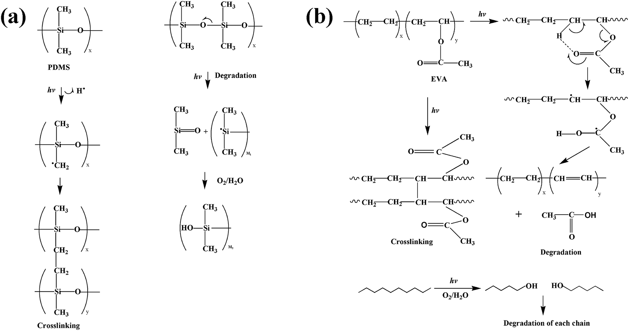 | ||
| Fig. 9 Schematic illustration of the mechanism of crosslinking and degradation of (a) PDMS and (b) EVA under UV radiation. | ||
For ultraviolet (UV) radiation the photon energy is sufficient to cause ionization, it means that, this radiation is capable of breaking chemical bonds. However compared to other ionization radiations like an electron beam, X-rays and γ rays with higher frequencies, the photon energy associated with UV radiation is significantly less. So its effect on a polymer is comparatively much less, and the process of polymer modification/degradation by UV rays is rather slow. However the photon energy associated with UV radiation is capable of breaking the chemical bonds present in a polymer. In silicone rubber mainly three types of bonds exist and their breaking energy is also in the following order, C–H (∼337.2 kJ mol−1) < C–C (∼607 kJ mol−1) < Si–O–Si (∼798 kJ mol−1). So the probability of breaking C–H is the most and the breaking of this bond in PDMS leads to the crosslinking process, whereas breaking of the Si–O–Si leads to polymer degradation, it requires the highest energy and so this process will be the slowest one.45
However the breaking of Si–O–Si bonds means the breakdown of the backbone chains of the polymer which leads to a reduction in tensile strength and an elongation at the break. The breakdown of C–H bonds leads to the formation of crosslinks among the polymer chains resulting in the increase in the modulus and hardness as observed for some aged samples. In EVA the main chain consists of C–C linkages which have bond strength less than that of the Si–O–Si bonds present in the silicone elastomer (PDMS).
 | ||
| Fig. 10 Variation of (a) dielectric constant (ε′) at 50 Hz, (b) dielectric loss (ε′′) at 50 Hz and (c) surface resistivity under different kinds of accelerated aging. | ||
The changes in the surface resistivity for the different types of aged samples are shown in Fig. 10c. For samples aged under boiling water, the surface resistivity decreases to 2.3 × 10¹⁵ ohm cm from 2.5 × 10¹⁵ ohm cm (fresh sample) whereas due to heat aging, the surface resistivity decreases drastically to 1.3 × 10¹⁵ ohm cm and for UV aging to 1.1 × 10¹⁵ ohm cm. The reduction in surface resistivity and hydrophobicity due to aging under the different conditions has significant technical importance regarding the performance of polymeric insulators under high voltage conditions. In high voltage application that is under a high potential difference, electrical discharge (electrical tracking) can take place on the insulator surface. This electrical tracking depends on the surface resistivity which again depends on different extrinsic factors like the deposition of the pollutant, moisture or water droplets on the insulator surface, facilitating the formation of low resistance paths for electrical discharge. So long as the water droplets formed on the insulator surface remain isolated the tracking is difficult to take place. If these droplets coalesce and form a bigger or continuous water line, electrical tracking can easily take place (dry band arching). In PDMS based insulators, the low molecular weight (LMW) fragments of the polymer, can migrate to the surface and can keep the surface hydrophobic in nature thereby preventing the formation of the continuous water lines necessary for tracking. With aging the concentration of the LMW fragments decreases in the matrix as does their migration to the surface. The possibility of surface tracking becomes more probable with aging. This decrease in the LMW fractions with aging is more due to the UV aging compared to other types of aging as reflected from the degree of reduction in the contact angle.46
 | ||
| Fig. 11 Change in the contact angle of unaged and different types of aged samples. | ||
 | ||
| Fig. 12 Picture of the spreading of water droplets on the different insulator surfaces (a) fresh sample, (b) boiling water aged sample, (c) heat aged sample and (d) UV aged sample. | ||
The detrimental effects mentioned earlier convert the hydrophobic surfaces to hydrophilic ones through the removal of the LMW fractions of PDMS. The presence of EVA in the blend has also some negative effect on the hydrophobicity because of the phenomenon of the migration of the LMW fractions from the bulk to the surface, as happens in the case of PDMS but is absent for EVA. During the different types of accelerated aging, the loss of the LMW fragments makes the surface hydrophilic in nature.46 However, the decrement of hydrophobicity is found to be more during heat and UV aging than during aging under boiling water, due to the higher loss of the LMW fragments by these two types of accelerated aging.17,47–49
The developed compounds exhibit better tracking characteristics (higher tracking voltage) compared to the commercially available PDMS based insulation compounds (Fig. S3†).
When the composite sample with 6 phr filler loading is subjected to the different kinds of aging, some roughness generates on the surface of the aged samples. It can be visualized when a comparison is made between the surfaces of a sample before and after aging. The increase in the surface roughness is mainly because of the polymer degradation that occurred on the exposed surface subjected to boiling water, heat and UV radiation (Fig. 13a–c). In a neat sample, the polymer chains thoroughly wet (coat) the filler particles and a smooth surface is observed for the fresh sample. However after prolonged aging, the degraded polymer chains get easily removed leaving behind exposed filler particles which may be partially or wholly detached from the bulk exhibiting surface roughness. The effect of aging on the surface is more pronounced for UV aging (Fig. 13c), where the surface has been found to be much more rough compared to the surfaces of the samples subjected to boiling water and heat. The surface degradation is found to be the least for aging under boiling water, whereas the effect of heat aging is the intermediate. This indicates that during service, the UV radiation is the main detrimental factor for high voltage insulators working in an open atmosphere. This is further corroborated by AFM analysis done for the unaged and differently aged samples of the nanocomposite.
 | ||
| Fig. 13 FESEM micrographs of 6 phr nanosilica filled nanocomposites, under (a) boiling water, (b) heat and (c) UV aged. | ||
 | ||
| Fig. 14 AFM 3D images of 6 phr nanosilica filled (a) unaged, (b) boiling water, (c) heat and (d) UV aged samples. | ||
 | ||
| Fig. 15 Comparison root mean square height (Sq, nm) of the 6 phr nanosilica filled unaged and aged samples. | ||
With aging the hydrophobic characteristics of the insulator housing deteriorates, this is one of the most detrimental effects for the insulator when it works in the high voltage power transmission lines. Also with aging, the surface roughness increases with time thereby introducing and increasing the site for mechanical failure (stress raiser). As a result the mechanical properties for aged samples decrease with time as shown earlier. Under different aging conditions the size of these defects magnifies with time and the chance of the accumulation of extraneous materials like moisture, pollutant, salts and carbon particles on the insulator surface increases. All these external materials deposited on the sample adversely affect the surface electrical characteristics and thereby increase the probability of frequent electrical tracking on the insulator surface ultimately leading to the failure of both the polymeric insulator housing and the composite insulators. Defects and micro-void formation in the insulator housing also increases the chance of partial discharge under high voltage.
4. Summary and conclusions
A PDMS/EVA 60/40 (w/w) blend has been found to be the most suitable polymer matrix which can replace 100% PDMS for making insulator housing. This blend is found to be better than neat PDMS with respect to the mechanical properties and price. But the blend is inferior to neat PDMS with respect to the hydrophobicity.The decrease in the hydrophobicity of PDMS due to the blending with EVA can be compensated through the incorporation of nanosilica as a secondary filler in the composition. The addition of nanosilica is found to improve the mechanical properties, hydrophobicity, surface resistivity and electrical tracking voltage. The optimum loading of the secondary filler is found to be 6 phr, beyond which some properties deteriorate due to improper filler dispersion in the matrix polymer.
The losses in the mechanical properties, electrical properties and surface hydrophobicity are observed for the insulator samples subjected to different types of accelerated aging processes. Of all aging tests, the exposure to high intensity UV radiation is found to cause the maximum overall reduction in the properties. So it can be concluded that the atmospheric UV radiation from sunlight and corona discharge have the maximum detrimental effects on the polymeric insulator housing.
The severe surface cracking is observed during UV aging through the initial formation of micro-cracks on the surface which is responsible for the deterioration of the mechanical, electrical and hydrophobic characteristics of the insulator.
Acknowledgements
The authors are thankful to Research Designs and Standards Organization (RDSO), Lucknow, India for sponsoring the project under which this investigation was carried out.Notes and references
- M. R. Raghuveer, E. Kuffel, A. H. Qureshi and W. Opydo, IEEE Trans. Power Appar. Syst., 1978, 97, 1672–1679 CrossRef.
- C. Aubin, C. Houdret, R. Mailfert and L. Pargamin, IEEE Trans. Electr. Insul., 1981, 16, 290–296 CrossRef.
- H. Janssen, J. M. Seifert and H. C. Karner, IEEE Trans. Dielectr. Electr. Insul., 1999, 6, 651–659 CrossRef CAS.
- S. Kumara, I. R. Hoque, S. Alam, Y. V. Serdyuk and S. M. Gubanski, IEEE Trans. Dielectr. Electr. Insul., 2012, 19, 1076–1083 CrossRef.
- P. Charalampidis, M. Albano, H. Griffiths, A. Haddad and R. T. Waters, IEEE Trans. Dielectr. Electr. Insul., 2014, 21, 740–748 CrossRef.
- E. A. Cherney, IEEE Trans. Dielectr. Electr. Insul., 2005, 12, 1108–1115 CrossRef CAS.
- M. A. Pradeep, N. Vasudev, P. V. Reddy and D. Khastgir, J. Appl. Polym. Sci., 2007, 104, 3505–3516 CrossRef CAS PubMed.
- A. E. Vlastos and E. Sherif, IEEE Trans. Power Delivery, 1990, 5, 406–414 CrossRef CAS.
- G. Heger, H. J. Vermeulen, J. P. Holtzhausen and W. L. Vosloo, IEEE Trans. Dielectr. Electr. Insul., 2010, 17, 513–520 CrossRef CAS.
- J. Mackevich and M. Shah, IEEE Trans. Electr. Insul., 1997, 13, 5–12 CrossRef.
- A. E. Vlastos and S. M. Gubanski, IEEE Trans. Power Delivery, 1991, 6, 888–900 CrossRef CAS.
- T. Sorqvist and S. M. Gubanski, IEEE Trans. Dielectr. Electr. Insul., 1999, 6, 744–753 CrossRef CAS.
- H. Homma, T. Kuroyagi, K. Izumi, C. L. Mirley, J. Ronzello and S. A. Boggs, IEEE Trans. Dielectr. Electr. Insul., 1999, 6, 370–375 CrossRef CAS.
- H. Liu, G. A. Cash, R. D. Sovar, G. A. George and D. Birtwhistle, IEEE Trans. Dielectr. Electr. Insul., 2006, 13, 877–884 CrossRef CAS.
- J. G. Wankowicz, S. M. Gubanski and W. D. Lampe, IEEE Trans. Dielectr. Electr. Insul., 1994, 1, 604–614 CrossRef CAS.
- S. Kumagai and N. Yoshimura, IEEE Trans. Dielectr. Electr. Insul., 2001, 8, 673–678 CrossRef CAS.
- Y. Bok-Hee and H. Chan-Su, IEEE Trans. Dielectr. Electr. Insul., 2005, 12, 1015–1024 CrossRef.
- B. Venkatesulu and M. J. Thomas, IEEE Trans. Dielectr. Electr. Insul., 2011, 18, 418–424 CrossRef CAS.
- G. Bo, T. Youping, Z. Yiyang, L. Ruihai, Z. Fuzeng, X. Zhuo and L. Dong, IEEE Conf. Electr. Insul. Dielectr. Phenom., 2013, 430–433 Search PubMed.
- J. Jin, S. Chen and J. Zhang, Polym. Degrad. Stab., 2010, 95, 725–732 CrossRef CAS PubMed.
- J. P. Reynders, I. R. Jandrell and S. M. Reynders, IEEE Trans. Dielectr. Electr. Insul., 1999, 6, 620–631 CrossRef CAS.
- R. S. Gorur, G. G. Karady, A. Jagota, M. Shah and A. M. Yates, IEEE Trans. Power Delivery, 1992, 7, 525–538 CrossRef CAS.
- G. Camino, S. M. Lomakin and M. Lazzari, Polymer, 2001, 42, 2395–2402 CrossRef CAS.
- R. Forch, H. Schonheer and A. T. A. Jenkins, Surface Design: Applications in Bioscience and Nanotechnology, Wiley-VCH, Germany, 2009, p. 471 Search PubMed.
- I. O. Ucar, M. D. Doganci, C. E. Cansoy, H. Y. Erbil, I. Avramova and S. Suzer, Appl. Surf. Sci., 2011, 257, 9587–9594 CrossRef CAS PubMed.
- A. Mata, A. Fleischman and S. Roy, Biomed. Microdevices, 2005, 7, 281–293 CrossRef CAS PubMed.
- R. S. Gorur, S. Sundhara Rajan and O. G. Amburgey, IEEE Trans. Electr. Insul., 1989, 24, 713–716 CrossRef CAS.
- M. Ehsani, H. Borsi, E. Gockenbach, G. R. Bakhsahnde, J. Morshedian and N. Abedi, IEEE International Conference on Solid Dielectrics ICSD, Toulouse, France, 2004, vol. 1, pp. 431–434 Search PubMed.
- S. Ansorge, F. Schmuck and K. O. Papailiou, IEEE Trans. Dielectr. Electr. Insul., 2012, 19, 209–217 CrossRef CAS.
- J. V. Vas, B. Venkatesulu and M. J. Thomas, IEEE Trans. Dielectr. Electr. Insul., 2012, 19, 91–98 CrossRef CAS.
- S. Kumagai and N. Yoshimura, IEEE Trans. Dielectr. Electr. Insul., 2001, 8, 203–211 CrossRef CAS.
- H. Zhou, H. Wang, H. Niu, A. Gestos, X. Wang and T. Lin, Adv. Mater., 2012, 24, 2409–2412 CrossRef CAS PubMed.
- N. Garcia, E. Benito, P. Tiemblo, M. M. B. Hasan, A. Synytska and M. Stamm, Soft Matter, 2010, 6, 4768–4776 RSC.
- X. Tang, T. Wang, F. Yu, X. Zhang, Q. Zhu, L. Pang, G. Zhang and M. Pei, RSC Adv., 2013, 3, 25670–25673 RSC.
- A. Milionis, R. Ruffilli and I. S. Bayer, RSC Adv., 2014, 4, 34395–34404 RSC.
- A. H. El-Hag, L. C. Simon, S. H. Jayaram and E. A. Cherney, IEEE Trans. Dielectr. Electr. Insul., 2006, 13, 122–128 CrossRef CAS.
- E. J. Park, J. K. Sim, M.-G. Jeong, H. O. Seo and Y. D. Kim, RSC Adv., 2013, 3, 12571–12576 RSC.
- H. Amrollahi and M. Borhani, Int. J. Eng. Res., 2015, 4, 69–72 CrossRef.
- J.-J. Park, Trans. Electr. Electron. Mater., 2012, 13, 301–304 CrossRef.
- S. Hui, T. K. Chaki and S. Chattopadhyay, Polym. Eng. Sci., 2010, 50, 730–738 CAS.
- S. Ju, M. Chen, H. Zhang and Z. Zhang, eXPRESS Polym. Lett., 2014, 8, 682–691 CrossRef CAS.
- A. Das, K. W. Stöckelhuber, R. Jurk, M. Saphiannikova, J. Fritzsche, H. Lorenz, M. Klüppel and G. Heinrich, Polymer, 2008, 49, 5276–5283 CrossRef CAS PubMed.
- R. A. Khare, A. R. Bhattacharyya, A. R. Kulkarni, M. Saroop and A. Biswas, J. Polym. Sci., Part B: Polym. Phys., 2008, 46, 2286–2295 CrossRef CAS PubMed.
- Y. Liu, Z. Li and B. Du, Appl. Phys. Lett., 2014, 105, 102905 CrossRef PubMed.
- J. A. Dean, Lange’s Handbook of Chemistry, McGraw-Hill, Inc., New York, 1999, pp. 329–341 Search PubMed.
- Y. Hirano, T. Inohara, M. Toyoda, H. Murase and M. Kosakada, IEEE Trans. Dielectr. Electr. Insul., 2001, 8, 97–103 CrossRef CAS.
- M. Ali and R. Hackam, IEEE Trans. Dielectr. Electr. Insul., 2009, 16, 842–852 CrossRef CAS.
- M. Ali and R. Hackam, IEEE Trans. Dielectr. Electr. Insul., 2008, 15, 1368–1378 CrossRef CAS.
- H. Hillborg and U. W. Gedde, IEEE Trans. Dielectr. Electr. Insul., 1999, 6, 703–717 CrossRef CAS.
- G. Momen, M. Farzaneh and R. Jafari, Appl. Surf. Sci., 2011, 257, 6489–6493 CrossRef CAS PubMed.
- P. K. Maji and A. K. Bhowmick, J. Appl. Polym. Sci., 2013, 127, 4492–4504 CrossRef CAS PubMed.
Footnote |
| † Electronic supplementary information (ESI) available: TEM, AFM and electrical tracking. See DOI: 10.1039/c5ra08277c |
| This journal is © The Royal Society of Chemistry 2015 |