MACl enhanced electron extraction in all-inorganic Cs2AgBiBr6 perovskite photovoltaics†
Jinxia
Duan
ab,
Yi
Yang
 a,
Jie
Tang
a,
Houzhao
Wan
a,
Jie
Tang
a,
Houzhao
Wan
 ab,
Guokun
Ma
ab,
Liangping
Shen
ab,
Jun
Zhang
ab,
Hao
Wang
ab,
Guokun
Ma
ab,
Liangping
Shen
ab,
Jun
Zhang
ab,
Hao
Wang
 *ab and
Hai
Zhou
 *ac
*ac
aSchool of Microelectronics, Hubei University, Wuhan 430062, P. R. China. E-mail: wangh@hubu.edu.cn
bHubei Yangtze Memory Laboratories, Wuhan 430205, P. R. China
cInternational School of Microelectronics, Dongguan University of Technology, Dongguan, Guangdong 523808, P. R. China. E-mail: hizhou@dgut.edu.cn
First published on 4th January 2023
Abstract
We present organic-halide treatment in advance to maximize electron extraction of Cs2AgBiBr6 double perovskite solar cells. Through optimizing the organic halide and concentration systematically, the best carbon-based Cs2AgBiBr6 perovskite solar cell fabricated in an airing chamber achieves a power conversion efficiency of 2.03% and shows excellent long-term stability in air over 30 days.
Halide perovskite materials have become one of the most competitive photovoltaic materials owing to their exceptional photoelectrical characteristics, such as large absorption coefficient, adjustable bandgap, high carrier mobility and long carrier diffusion length. Representative organic–inorganic hybrid perovskite solar cells (PeSCs) show outstanding photoelectric conversion ability. To date, the power conversion efficiency (PCE) has leapt to 25.8% (certified 25.5%).1,2 Unfortunately hybrid PeSCs contain lead and organic ions, resulting in poor device stability and environmental toxicity, which seriously hinder large-scale production and commercialization of PeSCs. Inorganic cations replacing organic cations and two heterovalent cations taking over divalent lead ions have been proposed to enhance the inherent stability and decrease heavy metal toxicity.3–6 The concept of a fully inorganic lead-free double perovskite with the formula of A2B+B′3+X6 conforms to this situation. According to the first principle calculation, Cs2AgBiBr6 is a double perovskite alternative to toxic and unstable hybrid PeSCs because of its high stability and long carrier lifetime.6–8
Slavney et al.9 presented that Cs2AgBiBr6 had terrible potential optical and physical properties, which motivated further exploration of double perovskites for photovoltaic applications. Greul et al. prepared Cs2AgBiBr6 films by a spin-coating method and incorporated them into photovoltaic devices in 2017.10 The Cs2AgBiBr6-based PeSC showed PCE of 2.43% and open circuit voltage (Voc) exceeding 1 V, which was the highest Voc for perovskite containing bismuth at that time. This work pointed out a promising class of perovskites for the photovoltaic field. However, the efficiency of Cs2AgBiBr6 PeSCs was limited by their wide indirect bandgap and high inherent defects. Increasing the light capture and crystalline quality of Cs2AgBiBr6 film is a considerable challenge to further improve Cs2AgBiBr6 device performances.10–13 Photosensitizers (such as dyes and organic materials) have been introduced to broaden the absorption spectrum and raise the device PCE of Cs2AgBiBr6 perovskite.11–13 For example, Yang et al.11 used an N719 interlayer to broaden the absorption and heighten the PCE to 2.84%. Wang et al.12 improved the light absorption of Cs2AgBiBr6 films by D149 dye treatment of the electron transport layer (ETL). Nevertheless, dye intermediates failed to improve the poor crystallinity of Cs2AgBiBr6 itself, and affect the internal resistance of the device, resulting in the decrease of the fill factor (FF).
In addition, expensive organic hole transport materials (HTMs) are very vulnerable to the migration of halide ions.14 The carbon electrode materials replacing the HTM and metal electrode are relatively mature in related fields. Cs2AgBiBr6 PeSCs based on carbon electrodes have seen some attempts.15,16 For example, Li et al. fabricated a Cs2AgBiBr6 PeSC with the efficiency of 2.57% and excellent high-temperature and air stability.15 Li et al.16 employed ionic liquids (ILs) to inhibit Br− migration effectively, thereby reducing film defects and improving energy level matching. A carbon-based Cs2AgBiBr6 PeSC achieved a PCE of 2.22% and positive long-term stability. These provide convenient and efficient strategies to raise the efficiency and stability of environmentally friendly Cs2AgBiBr6-based photovoltaics.
Undesirable performances of Cs2AgBiBr6 photovoltaics are due to their deep electron defects.15,17 The passivation for the ETL/perovskite interface by methylammonium chloride is an aid to improve the crystallization of Cs2AgBiBr6 film and electron extraction capability.18,19 In this work, we introduce methylammonium halide (MAX) to ameliorate the ETL/perovskite interface and perovskite quality. Three MAXs are employed to explore systematically the role of charge transport and perovskite crystallization.
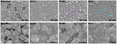
The concentration of the Cs2AgBiBr6 precursor solution is 0.5 M. After finishing the growth of TiO2 NRs, 0.25 M-MAX solution was spin-coated in advance on the TiO2 ETL followed by spin-coating the Cs2AgBiBr6 precursor. The entire preparation procedure of Cs2AgBiBr6 film was carried out in an airing chamber and drawn with a diagram in Fig. S1 (ESI†). Cs2AgBiBr6 films with uniform yellow appearance (optical image illustration is in Fig. S1, ESI†) were obtained after 280 °C annealing. Cs2AgBiBr6 film without pre-treatment was prepared as a reference sample. In order to verify the effect of MAX pre-treatment on the morphologies of Cs2AgBiBr6 films, the surface of the samples was observed by a Scanning Electron Microscope (SEM). SEM images of Cs2AgBiBr6 films with MAX pre-treatment (including the reference, MACl, MABr and MAI pre-treatment) were exhibited in Fig. 1 using low magnification and high magnification. Cs2AgBiBr6 samples with MACl, MABr and MAI pre-treatment were named Cs2AgBiBr6-MACl, Cs2AgBiBr6-MABr and Cs2AgBiBr6-MAI, respectively. From SEM images, rather more regular grains were observed in Cs2AgBiBr6 films with MAX pre-treatment than reference Cs2AgBiBr6. Among four Cs2AgBiBr6 films, Cs2AgBiBr6-MACl has the smoothest surface and the most uniform grains. The pin-holes and/or cracks were marked by circles in other Cs2AgBiBr6 films.
In the X-ray diffraction (XRD) spectra of Fig. S2a (ESI†), all samples presented Cs2AgBiBr6 characteristic peaks.13,15 The full-width half-maximum (FWHM) of the reference, Cs2AgBiBr6-MACl, Cs2AgBiBr6-MABr and Cs2AgBiBr6-MAI was 0.131°, 0.124°, 0.128° and 0.126° based on the (220) plane at ∼22.12°. The narrow FWHM of Cs2AgBiBr6-MACl suggested its largest grain size among the four Cs2AgBiBr6 samples,12 which was in accordance with the SEM observation in Fig. 1. Fig. S2b (ESI†) displays the ultraviolet-visible (UV-vis) absorption spectra of the Cs2AgBiBr6 samples. The absorption peak was at ∼439 nm for the Cs2AgBiBr6 samples. The absorption intensity followed the order: Cs2AgBiBr6-MACl > Cs2AgBiBr6-MAI > Cs2AgBiBr6-MABr > the reference. Cs2AgBiBr6-MACl had the highest absorption intensity and the broadest absorption edge. The bandgap energy calculation is shown in the Tauc diagram of Fig. S2b (ESI†). Cs2AgBiBr6-MACl had narrow direct and indirect bandgaps. Steady-state photoluminescence (PL) spectra in Fig. S2c (ESI†) showed that all Cs2AgBiBr6 samples had an emission peak at ∼520 nm, according to the direct bandgap. TiO2/Cs2AgBiBr6-MACl film had the lowest emission, which suggested its high crystalline quality and low defect density.15,20 Fig. S2d (ESI†) exhibits the time resolved photoluminescence (TRPL) spectra of TiO2/Cs2AgBiBr6 films. The carrier recombination lifetime (τ) fitting data are displayed in Table S1 (ESI†). The lifetime of the reference, Cs2AgBiBr6-MACl, Cs2AgBiBr6-MABr and Cs2AgBiBr6-MAI samples was 59.46 ns, 42.53 ns, 48.53 ns and 45.0 ns, respectively. The smallest lifetime of Cs2AgBiBr6-MACl indicated its fast electron transfer and low trap recombination.21 To elucidate the chemical state of Cs2AgBiBr6 films, the X-ray photoelectron spectroscopy (XPS) spectra are shown in Fig. S3 and S4 (ESI†). The expected elements were found in scanning XPS measurement of the Cs2AgBiBr6 films.20 The orbital binding energy of element Ag, Bi and Br for Cs2AgBiBr6-MACl shifted slightly towards the high binding energy direction, while the binding energy of Cs3d did not shift. The chemical bonding interaction of Cs-Br, Br-Bi and Br-Ag was enhanced for Cs2AgBiBr6-MACl, verified by Fourier transform infrared (FT-IR) measurement. This was beneficial to improving the stability of Cs2AgBiBr6 PeSCs.
| Device structure | PCE | Fabrication | Long-term stability | Ref. |
|---|---|---|---|---|
| FTO/m-TiO2/Cs1.99Li0.01Cs2AgBiBr6/C | 2.57% | N2 glove box | 80%, 25 °C, 5%RH, 90 days | 15 |
| 80%, 85 °C, 0%RH, 60 days | ||||
| FTO/TiO2NRs/Cs2(Ag1−xZnx)BiBr6/C | 2.16% | N2 glove box | 90%, 25 °C, 40%RH, 14 days in ambient air | 21 |
| FTO/TiO2NRs/BMPyrCl/Cs2AgBiBr6/C | 2.22% | N2 glove box | ∼100%, 25 °C, 40% ± 5%RH, 40 days in ambient air. | 16 |
| FTO/m-TiO2/Cs2AgBiBr6/SnS QDs/C | 1.95% | N2 glove box | 90%, 42 h in ambient air. | 23 |
| FTO/TiO2NRs/Cs2AgBiBr6-MACl/C | 2.03% | Airing chamber | 90%, 28 °C, 50%–60%RH, 30 days in ambient air | This work |
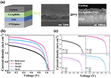
HTM-free PeSCs using carbon as the top electrode were fabricated with the structure of FTO/TiO2/Cs2AgBiBr6/carbon. A typical diagrammatic sketch and cross-sectional image of the Cs2AgBiBr6-MACl device are shown in Fig. 2a. The J–V curves of the Cs2AgBiBr6 devices are depicted in Fig. 2b. The Cs2AgBiBr6-MACl PeSC had a significantly improved short-circuit current density (Jsc) of 3.04 mA cm−2 and FF of 62% compared to the reference PeSC, resulting in the efficiency reaching 2.03%. The efficiency of the Cs2AgBiBr6 devices was in the order of Cs2AgBiBr6-MACl > Cs2AgBiBr6-MAI > Cs2AgBiBr6-MABr > the reference. The PCE of the Cs2AgBiBr6-MACl device is the highest, which is 68% higher than that of the reference PeSC. The best and average photovoltaic parameters of the Cs2AgBiBr6 devices are summarized in Table S2 (ESI†). As shown in Fig. 2c, the reverse and forward scanning (RE and FW) J–V curves were diagrammed for the champion devices. The hysteresis index (HI) was further quantified according to the formula21
| HI = [JRE(0.8 Voc) − JFW(0.8 Voc)]/JFW(0.8 Voc) | (1) |
 | ||
| Fig. 2 (a) Scheme and SEM sectional images of the device structure. (b) J–V curves of the champion devices. (c) RE and FW J–V curves for the best devices. | ||
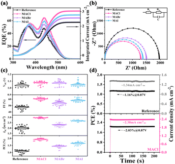
Fig. 3a portrays the external quantum efficiency (EQE) spectra of the Cs2AgBiBr6 PeSCs. In the wavelength range of 350–550 nm, the Cs2AgBiBr6-MACl PeSC had the highest EQE value among the four Cs2AgBiBr6 cells. The EQE of the Cs2AgBiBr6-MACl PeSC was 65% at 440 nm, which was 15% more than that of the reference PeSC. The calculated integral current density was from 2.27 mA cm−2 in the reference PeSC to 3.01 mA cm−2 in the Cs2AgBiBr6-MACl device, which corresponded to the J–V results in Fig. 2b. The Cs2AgBiBr6-MACl device obtained the highest current density. To further explore the raised FF and Jsc related to charge transport at the interface and interior of the PeSCs, electrochemical impedance spectroscopy (EIS) tests were carried out. Nyquist spectra of four PeSCs were plotted in Fig. 3b and the corresponding equivalent circuit was illustrated. The fitted data are summarized in Table S3 (ESI†), where Rs represents the series resistance of the devices, Rct is the interfacial charge transport resistance and C refers to the capacitance. Rct was arranged in the following order: the reference > Cs2AgBiBr6-MABr > Cs2AgBiBr6-MAI > Cs2AgBiBr6-MACl. The Rct values were calculated to be 1.99 kΩ, 1.51 kΩ, 1.36 kΩ and 1.27 kΩ, respectively. Significantly reduced Rct indicates superior charge collection, rendering improved FF and diminished HI in the Cs2AgBiBr6-MACl and Cs2AgBiBr6-MAI devices.12,16 Hence, Cs2AgBiBr6-MACl had the champion efficiency combined with the highest Jsc. The statistical photovoltaic parameters of the Cs2AgBiBr6 devices were summarized in Table S2 (ESI†) and Fig. 3c. The increase of Jsc and FF produced high PCE in the Cs2AgBiBr6-MACl devices. To verify whether the PeSCs stabilize the output power under the irradiation of AM1.5G standard sunlight, the steady-state photocurrent and efficiency at the maximum power point (MPP) were further characterized in the air environment, as shown in Fig. 3d. The voltage at the maximum power point (Vmpp) of the Cs2AgBiBr6-MACl device was 0.87 V, and the steady Jsc and PCE are 2.38 mA cm−2 and 2.03%, which were much higher than those of the reference device (1.34 mA cm−2 and 1.16%). The photoelectric conversion curves of the MAX pre-treated devices under continuous light within 200s were smoother than that of the reference device, indicating better interface contact of ETL/perovskite in the PeSCs with MAX pre-treatment. The trap density (Ntrap) was calculated by the space charge limited current (SCLC) model to be 1.468 × 10¹⁵ m−3, 9.737 × 10¹⁴ m−3, 1.312 × 10¹⁵ m−3 and 1.27 × 10¹⁵ m−3 for the reference, Cs2AgBiBr6-MACl, Cs2AgBiBr6-MABr and Cs2AgBiBr6-MAI, respectively. The dark J–V curves were measured and plotted in Fig. S8 (ESI†) to unravel the working mechanism of the devices. The Cs2AgBiBr6-MACl PeSC had the lowest saturation current and relatively large shunt resistance (Rsh) among the four Cs2AgBiBr6 devices, which suggested that the Cs2AgBiBr6-MACl PeSC had high electron extraction and low defect recombination. This was in line with the absorption, PL, EIS, defect and J–V results.
Based on these results, the mechanism of Cs2AgBiBr6-MACl was speculated. At the initial stage, MA+ and Cl− ions participated in the double perovskite crystallization, producing the formation of Cs2−xMAxAgBiBr6−yCly (0 < x < 1.0, 0 < y < 1.0) intermediate phase. With the volatilization of MA+ and Cl− ions during heat treatment, the Cs2−xMAxAgBiBr6−yCly intermediate phase transformed to the ultimate Cs2AgBiBr6. Adequate volatile additive can promote crystal growth, which resulted in superior film morphology by altering the activation energy of the perovskite crystallization.22,23 Consequently, MACl delayed the crystallization progression of Cs2AgBiBr6 perovskites, resulting in large grain sizes and low trap density for Cs2AgBiBr6-MACl. Moreover, the strong MA+/TiO2 interaction compared to inorganic ion/TiO2 brought higher quality double perovskite film and faster electron extraction in the perovskite PeSC.19 Impurity phase containing chlorine caused by excess MAX would hinder charge transport, which was confirmed by the inferior performance of Cs2AgBiBr6-0.5MACl (shown in Fig. S9, ESI†).
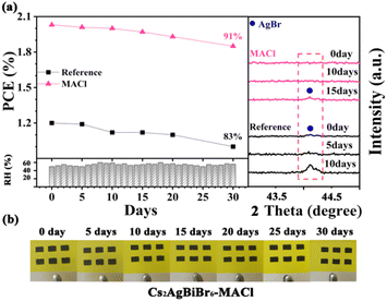
In order to investigate the effect of MACl pre-treatment on the performance stability of the PeSCs, the unpackaged reference and Cs2AgBiBr6-MACl samples were monitored by storing them under the air condition of 28 °C and relative humidity of 50–60% for 30 days. The PCE and XRD results are shown in Fig. 4a and Table S5 (ESI†). By tracking the PCE changes of the PeSCs, the Cs2AgBiBr6-MACl device maintained more than 90% of the initial PCE, while the reference device maintained 83% of the initial efficiency. AgBr miscellaneous phase was detected for the reference on the fifth day and aggravated on the tenth day by XRD monitoring in Fig. 4a, which was considered as an evil to deteriorate device performance. AgBr impure phase appeared after 15 days for the Cs2AgBiBr6-MACl device. No significant change of the Cs2AgBiBr6-MACl film was monitored in the appearance during preservation, which was displayed in photos of the samples during storing for 30 days. The Cs2AgBiBr6-MACl sample had better stability because of its higher perovskite crystalline degree than the reference sample. In addition, the hydrophobicity of the carbon electrode provides protection for the perovskite films, which further improves the environmental stability of the Cs2AgBiBr6 PeSCs. The entire preparation process being completed in air widened the application fields of Cs2AgBiBr6 perovskite (Table 1).
In summary, we fabricated efficient and stable Cs2AgBiBr6 PeSCs by introducing MAX pre-treatment to modify the ETL/Cs2AgBiBr6 interface and perovskite crystalline quality. The Cs2AgBiBr6 with three MAX pre-treatment was studied in an airing chamber systematically. The MACl modifier can bond with the ETL and perovskite and enhance perovskite crystallization. MACl modification facilitated electron extraction from the perovskite to the ETL, which reduced the trap-assisted recombination. As a result, the optimized PeSC with Cs2AgBiBr6-MACl achieved a PCE of 2.03% with slightly higher Jsc and FF than the reference device. Importantly, Cs2AgBiBr6-MACl exhibited better durability of the resultant PeSCs.
This research was aided financially by the National Natural Science Foundation of China (No. 11874143, 51972101), Hubei Provincial Department of Education of China (No. D20191005) and Application Fundamental Research Project of Wuhan Science and Technology Bureau (No. 2019010701011396).
Conflicts of interest
There are no conflicts to declare.Notes and references
- M. Kim, J. Jeong, H. Lu, T. K. Lee, F. T. Eickemeyer, Y. Liu, I. W. Choi and S. J. Choi, et al. , Science, 2022, 375, 302–306 CrossRef CAS PubMed.
- L. Zhang, X. Pan, L. Liu and L. Ding, J. Semicond., 2022, 43, 030203 CrossRef.
- B. Wu, W. Ning, Q. Xu, M. Manjappa, M. Feng, S. Ye, J. Fu and S. Lie, et al. , Sci. Adv., 2021, 7, eabd3160 CrossRef CAS PubMed.
- Z. Fang, S. Wang, S. Yang and L. Ding, Inorg. Chem. Front., 2018, 5, 1690–1693 RSC.
- W. Hu, X. He, Z. Fang, W. Lian, Y. Shang, X. Li, W. Zhou and M. Zhang, et al. , Nano Energy, 2020, 68, 104362 CrossRef CAS.
- M. T. Sirtl, R. Hooijer, M. Armer, F. G. Ebadi, M. Mohammadi, C. Maheu, A. Weis, B. T. van Gorkom, S. Häringer, R. A. J. Janssen, T. Mayer, V. Dyakonov, W. Tress and T. Bein, Adv. Energy Mater., 2022, 12, 2103215 CrossRef CAS.
- W. Tress and M. T. Sirtl, Sol. RRL, 2021, 6, 2100770 CrossRef.
- X. Cai, Y. Zhang, Z. Shi, Y. Chen, Y. Xia, A. Yu, Y. Xu, F. Xie, H. Shao, H. Zhu, D. Fu, Y. Zhan and H. Zhang, Adv. Sci., 2022, 9, e2103648 CrossRef PubMed.
- A. H. Slavney, T. Hu, A. M. Lindenberg and H. I. Karunadasa, J. Am. Chem. Soc., 2016, 138, 2138–2141 CrossRef CAS PubMed.
- E. Greul, Michiel L. Petrus, A. Binek, P. Docampo and T. Bein, J. Mater. Chem. A, 2017, 5, 19972–19981 RSC.
- X. Yang, Y. Chen, P. Liu, H. Xiang, W. Wang, R. Ran, W. Zhou and Z. Shao, Adv. Funct. Mater., 2020, 30, 2001557 CrossRef CAS.
- L. Yang, P. Hou, B. Wang, C. Dall'Agnese, Y. Dall'Agnese, G. Chen, Y. Gogotsi, X. Meng and X.-F. Wang, Chem. Eng. J., 2022, 446, 136963 CrossRef CAS.
- B. Wang, N. Li, L. Yang, C. Dall’Agnese, A. K. Jena, S. I. Sasaki, T. Miyasaka, H. Tamiaki and X. F. Wang, J. Am. Chem. Soc., 2021, 143, 2207–2211 CrossRef CAS PubMed.
- Q. Dou, T. Whatley, T. Syed, W. Wei and H. Wang, J. Mater. Chem. A, 2022, 10, 19211–19230 RSC.
- J. Li, J. Duan, J. Du, X. Yang, Y. Wang, P. Yang, Y. Duan and Q. Tang, ACS Appl. Mater. Interfaces, 2020, 12, 47408–47415 CrossRef CAS PubMed.
- J. Li, X. Meng, Z. Wu, Y. Duan, R. Guo, W. Xiao, Y. Zhang, Y. Li, Y. Shen, W. Zhang and G. Shao, Adv. Funct. Mater., 2022, 32, 2112991 CrossRef CAS.
- F. Ji, Y. Huang, F. Wang, L. Kobera, F. Xie, J. Klarbring, S. Abbrent, J. Brus, C. Yin, S. I. Simak, I. A. Abrikosov, I. A. Buyanova, W. M. Chen and F. Gao, Adv. Funct. Mater., 2020, 30, 2005521 CrossRef CAS.
- F. Ye, J. Ma, C. Chen, H. Wang, Y. Xu, S. Zhang, T. Wang, C. Tao and G. Fang, Adv. Mater., 2021, 33, e2007126 CrossRef PubMed.
- H. Wu, Y. Wang, A. Liu, J. Wang, B. J. Kim, Y. Liu, Y. Fang, X. Zhang, G. Boschloo and E. M. J. Johansson, Adv. Funct. Mater., 2021, 32, 2109402 CrossRef.
- P. Hou, W. Yang, N. Wan, Z. Fang, J. Zheng, M. Shang, D. Fu, Z. Yang and W. Yang, J. Mater. Chem. C, 2021, 9, 9659–9669 RSC.
- J. Duan, Q. Yue, Q. Xiong, L. Wang, L. Zhu, K. Zhang, J. Zhang and H. Wang, Appl. Surf. Sci., 2019, 470, 613–621 CrossRef CAS.
- Y. Ou, Z. Lu, J. Lu, X. Zhong, P. Chen, L. Zhou and T. Chen, Opt. Mater., 2022, 129, 112452 CrossRef CAS.
- Y. Ou, J. Lu, X. Zhong, X. Li, S. Wu, P. Chen and L. Zhou, Mater. Lett., 2022, 312, 131672 CrossRef CAS.
Footnote |
| † Electronic supplementary information (ESI) available. See DOI: https://doi.org/10.1039/d2cc06432d |
| This journal is © The Royal Society of Chemistry 2023 |


