 Open Access Article
High-performance polymer field-effect transistors: from the perspective of multi-level microstructures
Ze-Fan
Yao
 ,
Jie-Yu
Wang
and
Jian
Pei
 *
*
Beijing National Laboratory for Molecular Sciences (BNLMS), Key Laboratory of Polymer Chemistry and Physics of Ministry of Education, Center of Soft Matter Science and Engineering, College of Chemistry and Molecular Engineering, Peking University, Beijing 100871, China. E-mail: jianpei@pku.edu.cn
First published on 24th December 2020
Abstract
The multi-level microstructure of conjugated polymers is the most critical parameter determining the charge transport property in field-effect transistors (FETs). However, controlling the hierarchical microstructures and the structural evolution remains a significant challenge. In this perspective, we discuss the key aspects of multi-level microstructures of conjugated polymers towards high-performance FETs. We highlight the recent progress in the molecular structures, solution-state aggregation, and polymer crystal structures, representing the multi-level microstructures of conjugated polymers. By tuning polymer hierarchical microstructures, we attempt to provide several guidelines for developing high-performance polymer FETs and polymer electronics.
Introduction
Conjugated polymers and polymer-based field-effect transistors (FETs) have attracted increasing interest over the past decades.1–7 Polymer FETs are considered as an essential component of future electronics beyond the commercial silicon-based integrated circuits, especially in wearable devices and flexible electronics.8–10 The carrier mobility is a critical parameter to assess the FET performance and charge transport properties of conjugated polymers.11,12 With the painstaking efforts in molecular design, efficient synthesis, and device fabrication technology, the state-of-art mobility in polymer FETs reached 1 to 10 cm2 V−1 s−1, which surpasses that of the widely used amorphous silicon with the value of about 1 cm2 V−1 s−1.4,13 The high FET mobility helps achieve the conceivable potentials of conjugated polymers in high-frequency and low-power logic circuits.14,15 However, the lack of clarity on the microstructures of conjugated polymers fundamentally limits the understanding of charge transport and achieving superior electronic performance. Recently, considerable efforts have been devoted to improving polymer FET performance by controlling the molecular structures and film microstructures of conjugated polymers.In this perspective, we focus on the current challenges and the latest progress in polymer FETs. First, we summarize the ingenious molecular design strategies to develop high-performance conjugated polymers. Molecular-scale properties, such as oxidation/reduction potentials,16–19 conformational locking,20,21etc., can be finely controlled through these strategies. Although a discrete molecule's properties can be assumed or even predicted by molecular design and theoretical simulations, the situations for molecular assemblies and multi-level microstructures are much complicated.22 Hence, we introduce the central concept of multi-level microstructures of conjugated polymers, which is responsible for the charge transport features. Since most polymers require a solution process, we identify the importance of solution-state aggregation. From the solvated aggregates, solid-state microstructures can be well modulated for boosting their charge transport performance in FETs and solar cells.23–27 Finally, polymer crystals and crystal structures are practically useful for understanding the charge transport at molecular and atomic scales. It remains difficult to precisely elucidate the crystal structures of conjugated polymers.
From molecular structures to multi-level microstructures
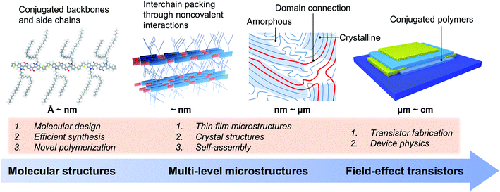
The charge transport and FET performance of conjugated polymers critically depend on their solid-state microstructures at various spatial scales (Fig. 1).28–31 That is, the charge transport properties are dominated by the microstructures containing multiple polymer chains, not a single polymer chain. At the molecular scale, conjugated polymers usually consist of rigid conjugated backbones and flexible alkyl side chains, which can be finely tuned by molecular design and chemical synthesis.3,4,17,32–34 Upon one single molecule, polymer chains arrange together by the cooperativity of noncovalent interactions, including π–π interactions between conjugated backbones and dispersion interactions between alkyl chains.21,35,36 In solution, conjugated polymer chains could form interchain aggregates due to the strong molecular interactions between polymer chains.37,38 These aggregates would be incorporated into the solid-state microstructures during the film formation process. Hence, tuning the self-assembly process of conjugated polymers from solution to thin films can achieve the desired solid-state microstructures for efficient charge transport.27,39–41Polymer crystals are practically useful for understanding the polymer packing modes and interchain charge transfer.42,43 However, obtaining the polymer crystals is quite difficult, further limiting the structural elucidation of conjugated polymers. While the thin films are fabricated, conjugated polymers usually form from-nanometre-to-micrometre crystalline and amorphous regimes at the same time (Fig. 1), making it difficult to characterize their microstructures. The connections between crystalline domains are typically satisfied by long polymer chains.29 Conjugated polymers are commonly used as the active semiconductor layer in FETs. The device architecture of FETs also has a significant impact on transistor performance. There are several issues of device physics in polymer FETs, e.g., nonideality, contact resistance, and carrier trapping, which are proven to be crucial for evaluating charge transport properties.12,13 Hence, we noted that comparison of carrier mobility requires careful elimination of these device issues, especially for unravelling the structure–property relationship. Otherwise, imprecise estimation of the carrier mobility of conjugated polymers would lead to inaccurate or even wrong molecular design strategies.
It is critical to control the multi-level microstructures and structural evolution towards high-performance conjugated polymers in FETs and other related electronic devices. The multi-level microstructures of conjugated polymers usually demand multiple characterization methods, such as X-ray techniques and microscopies. Revealing the structure–property relationship is essential to improve the device performance, which will promote the understanding of polymer chemistry and physics, and the development of emerging polymer applications. Therefore, the following part of this perspective focuses on the hierarchical microstructures of conjugated polymers towards high-performance polymer FETs, including molecular structures, solution-state aggregation, crystals, and crystal structures.
Molecular structures and design strategy
Since the 2000s, chemists have devoted excellent research work to the design and synthesis of high-performance conjugated polymers. Several robust design strategies endow polymers with specific and desirable properties. Due to the high ambient stability, p-type, i.e., hole transport, polymers are predominantly studied in the field of polymer FETs. With these strategies, the electron affinity of the polymer is tuned for stable n-type transport, i.e., electron transport.44 In this section, we summarize the representative molecular design strategies in dimensions down to molecular scales from Å to nm.In 1986, the first reported polymer FET was based on the directly electrochemically polymerized polythiophene. The transistor exhibited a p-type FET mobility up to 10−5 cm2 V−1 s−1.45 After that, the regioregular alkyl-substituted polymer poly(3-hexylthiophene) (P3HT) was adopted as the active layer, leading to improved solution processability, structural ordering, and a hole mobility of 0.01 cm2 V−1 s−1.46 In 1999, regioregular P3HT exhibited high mobilities of 0.1 cm2 V−1 s−1 using a self-organization strategy.6 Hexamethyldisilane was modified on the substrate to promote the polymer self-organization of edge-on orientation. Accordingly, the alkyl side chains can afford good solution processability; hence, the self-organization of the polymer chains can be achieved through the polymer organization and crystallization on the substrates.
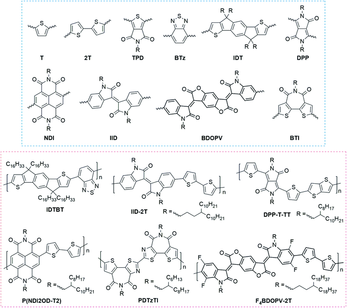
Donor–acceptor (DA) polymers represent the state-of-art high-performance conjugated polymers with FET carrier mobilities >1 cm2 V−1 s−1. Fig. 2 summarizes the most representative building blocks for high-performance FETs and the corresponding high-mobility DA polymers. In these polymers, oligothiophene motifs, such as thiophene (T) and bithiophene (2T), usually act as the donor segment because of their higher electron density. In contrast, the acceptor, including carbonyl, amide, halogen, etc., contains electron-withdrawing groups to decrease the electron density. Because of the distinct difference in electron density, donor and acceptor units commonly possess strong intermolecular interactions, leading to tight π–π contacts and enhanced interchain charge transport.
The molecular orbitals of donor and acceptor units reorganize to form the π orbitals of DA polymers. The strong electronic couplings between the donor and acceptor moieties contribute to delocalized π orbitals and lower energy gaps in charge transport and light absorption. Hence, small carrier effective masses and high carrier mobilities can be achieved in DA copolymers.47 Significantly, the electron affinity (EA), ionization potential (IP), and excited states of these derivative molecules and polymers are related to the oxidation/reduction properties and light absorption in the optoelectronic devices. EA and IP are closely related to the electron-poor and electron-rich moieties in DA polymers, respectively, which can be intuitively recognized according to their chemical structures. EA, IP, and excited states can be well predicted by density functional theory (DFT), guiding rational molecular design.48,49 It should be noted that the choice of DFT calculation methods needs careful evaluation when predicting the molecular properties. Related discussion can be found from several articles focusing on the DFT calculation of conjugated molecules and polymers.50,51
Introducing heteroatoms (nitrogen, chalcogen, halogen, etc.) in conjugated molecules and polymers is a practical approach to modulate the electronic structures and molecular packing, thus charge transport properties. For example, replacing a carbon atom with a nitrogen atom in benzene or thiophene produces more electron-deficient aromatic rings of pyridine and thiazole.52–54 Hence, energy levels of the conjugated segment can be finely tuned by chemical modification. Besides, the lone pair electrons of the heteroatoms can further form weak molecular interactions, locking the backbone conformation.20 For instance, fluorine and nitrogen atoms can form weak intramolecular F⋯H or N⋯H hydrogen bonds.55 Several other types of interactions, including F⋯S, S⋯N, and S⋯O, also contribute to the polymer backbone conformations.56,57 These weak interactions have binding energies ranging from 0.44 to 2.2 kcal mol−1, with an accumulative effect in polymer chains.35
Amidation and imidization are commonly used strategies to develop novel acceptor units in DA polymers.17 Several widely used building blocks were designed using this strategy (Fig. 2), such as thieno[3,4-c]pyrrole-4,6-dione (TPD), diketopyrrolopyrrole (DPP), naphthalene diimide (NDI), isoindigo (IID), benzodifurandione-based oligo(p-phenylene vinylene) (BDOPV), and bithiophene diimide (BTI). Amidation and imidization of conjugated units can not only lower the energy levels, making a transition from p-type polymers to n-type polymers, but also lock the corresponding torsional angles, reducing the conformational disorder. For example, two imide groups in the DPP unit lock the torsional angles of a butadiene unit;58 the imide group in BTI locks the rotatable torsional angle between the two thiophene rings.59
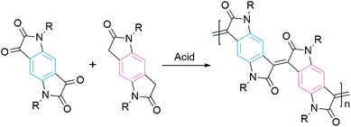
Most of the DA polymers are typically synthesized by metal-mediated coupling reactions, resulting in single-bond connections between conjugated segments. These rotatable single bonds in the conjugated backbone would lead to conformational and energetic disorders. Usually, a large disorder limits the charge transport. Onwubiko et al. reported a new polymerization method based on the aldol condensation reaction (Fig. 3).60 The aldol-condensed polymers possessed double-bond connections and confined backbone conformations. These rigid polymers exhibited air stable electron transport in FETs with mobility ranging from 10−5 to 0.2 cm2 V−1 s−1.60,61 Lu et al. n-doped aldol-condensed polymers and achieved stable conductivities of up to 1.1 S cm−1, suggesting their potential application in organic thermoelectrics.62
Side chains of conjugated polymers have been found to aid dissolution due to their conformational entropy change. However, the side chains in conjugated molecules and polymers have been proven to be crucial for determining the solid-state microstructures, hence the charge transport performance.33,63–67 Pei and coworkers systematically studied the effect of the branching point of the widely used side chains in isoindigo-based polymers.64 The conjugated backbone stacked more tightly with reduced π–π distances while moving the branching point further from the backbone, leading to enhanced mobilities. Similar effects of branching point were also reported in DPP-based and BDOPV-based polymers.68,69 Mei et al. reported an isoindigo-based conjugated polymer with a designed siloxane-terminated solubilizing group as the side chain.65 The polymer exhibited a short π–π stacking distance of 3.58 Å, leading to efficient interchain charge transport and hole mobility of 2.00 ± 0.49 cm2 V−1 s−1. Inspired by Mei's work, Yang and Oh demonstrated a hybrid side-chain strategy in DPP-based polymers. They achieved hole and electron mobilities of 3.97 and 2.20 cm2 V−1 s−1, respectively, in DPP-based polymers with selenophene units in the main backbone and siloxane-terminated hexyl in side chains.66 Kim and Cho demonstrated a highly ordered polymer packing of NDI-based conjugated polymers by utilizing semifluoroalkyl side chains.70 In these polymer films, strong self-organization of the semifluoroalkyl chains induced the backbone to form highly ordered packing, i.e., the backbone and side chains were nearly crystals. Hence, the tight polymer packing resulted in a high electron mobility of 6.50 cm2 V−1 s−1. Anthopoulos and Patil demonstrated copolymerization of alkyl-DPP with triethylene glycol (TEG)-DPP. The DPP-based copolymer exhibited near-infrared absorption and high electron mobility of 3 cm2 V−1 s−1.71 Due to the excellent compatibility with ions, the ethylene glycol side chains have recently been adopted in polymers for organic thermoelectrics (OTEs)72,73 and organic electrochemical transistors (OECTs).74,75
Crystalline polymers are expected to exhibit excellent FET performance; however, the long-range crystalline packing structures are not necessary for several polymers, such as indacenodithiophene-co-benzothiadiazole (IDTBT). IDTBT is a near-amorphous conjugated polymer with low degrees of energetic disorder and high carrier mobility up to 3.6 cm2 V−1 s−1.76,77 Although IDTBT shows a near-amorphous microstructure, the backbone conformation is ordered and resilient to packing disorder. The efficient charge transport in IDTBT is quasi one-dimensional along the conjugated backbones, suggesting disorder-free transport.78 Therefore, the backbone conformation or long-range packing orders can lead to efficient charge transport in conjugated polymers.
The molecular weight of a polymer and its distribution (polydispersity) also critically affect the FET performance.79 Low-molecular-weight polymer chains can aggregate and form ordered crystalline domains, while high-molecular-weight polymers can connect the domains and contribute to an interconnected network.29 Hence, the existence of low- and high-molecular-weight chains (i.e., controlled polydispersity) benefits the development of high-performance polymer FETs.80–82
In Fig. 4a, we summarize the primary aspects of molecular design strategies for high-performance conjugated polymers. These strategies have a synergetic effect on polymer microstructures and properties. As a case, we choose F4BDOPV-2T to illustrate the above molecular design strategies (Fig. 4b).83 F4BDOPV-2T is a recently developed high-performance n-type conjugated polymer. F4BDOPV-2T exhibited air-stable electron mobilities ranging from 1 to 14 cm2 V−1 s−1 depending on the fabrication conditions.40,83 F4BDOPV-2T consisted of three main parts: donor and acceptor conjugated units and a carefully selected alkyl side chain of 4-octadecyldocosyl. (1) A large electron-deficient F4BDOPV core was supported by four carbonyl groups and four fluorine atoms, leading to lower electron levels and strong interactions with the electron-rich bithiophene. (2) The backbone conformation was locked by several intramolecular interactions, including F⋯H hydrogen bonds and F⋯S interactions, leading to a rigid backbone conformation and sufficient interchain electronic coupling.83,84 (3) The alkyl side chain affords good solubility in organic solvents. Simultaneously, the branch point of the alkyl chains is tuned to achieve better interchain π–π stacking.
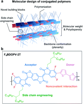 | ||
| Fig. 4 (a) Molecular design strategies for developing high-performance conjugated polymers. (b) A representative polymer, F4BDOPV-2T, is shown as an example. | ||
Beyond molecular structure design, fabrication techniques and device engineering simultaneously determine a polymer's solid-state microstructures and thereby transistor performances. In the following parts, we focus on the solution-state aggregation of conjugated polymers and its effects on solid-state microstructures and charge transport properties.
Solution-state aggregation
Solution-state aggregation of conjugated polymers is a general phenomenon due to the strong interactions between polymer chains. Since polymers usually require a solution process to fabricate thin films for FET devices, it is crucial to unravel and control solution-state aggregation. While the polymer forms aggregates in solution, the film-formation would be governed by further growth of polymer aggregates. Simultaneously, the chain packed structures in the solvated aggregates will be incorporated into the solid-state microstructures. However, adequate characterization and modulation methods of polymer solution-state aggregation are lacking. Several recent studies have demonstrated that controlling the solution-state aggregation of conjugated polymers benefits the formation of specific solid-state microstructures for high-performance polymer electronics.In 1983, Heeger and coworkers studied the rod-to-coil conformational transition of a diacetylene polymer in solution.85 According to their light scattering experiments, the polymer exhibited coil-like structures with a small hydrodynamic radius in chloroform, generally a good solvent for conjugated polymers. While adding a poor solvent such as hexane, the hydrodynamic radius increased, implying that the polymer underwent transition to rigid rod conformations. In 1989, Aime et al. utilized small-angle neutron scattering (SANS) to determine the polymer chain structures of poly(3-butylthiophene), which confirmed that poly(3-butylthiophene) possesses positive interchain interactions in solution even at a low concentration of 0.1 g L−1.37 SANS is a suitable characterization method of solution-state structures of conjugated polymers due to the low absorption coefficient and high scattering difference between the organic solvent and polymer solute.86 In a word, light absorption and fluorescence, light, X-ray, and neutron scattering are the most used techniques for characterizing polymer solution-state aggregates. It is urgent to develop a direct method for observing polymer aggregates and their evolution, such as electron microscopy and scanning probe microscopy under solution conditions.87,88
The solvent has been proven to be critical to the solution-state aggregation and solid-state microstructures in a representative conjugated polymer, polyfluorene.90–92 Recently, Li et al. reported two different semi-crystalline polymorphs of a DPP-based polymer (D-PDPP4T-HD) via a mixed solvent strategy and their impact on the optoelectronic performance (Fig. 5).89 The ordered aggregates of D-PDPP4T-HD in pure chloroform (CF) were defined as the β1 phase. When adding 1,2,4-trichlorobenzene (TCB) into the chloroform solution of D-PDPP4T-HD, the polymer chains tended to disaggregate into the amorphous phase (α) and then form distinctly different ordered aggregates of the β2 phase (Fig. 5b). The transformation process was monitored and confirmed through comprehensive UV-vis-NIR absorption spectra and steady-state photoluminescence spectra (Fig. 5c). Along with the appearance of the emerging β2 phase, a new absorption peak emerges at 870 nm (Fig. 5d). The red shift in light absorption and emission of the polymer β2 phase indicates a small optical gap, resulting from the π electrons' delocalization. On the other hand, better delocalization implies the extended backbone conformation in the β2 phase, which would enhance the interchain interactions. Furthermore, the β2 phase was obtained in thin films deposited from the mixed CF:TCB solution. According to the grazing incidence wide-angle X-ray scattering (GIWAXS) of the thin films, polymer chains showed a shorter π–π distance in the β2 phase compared to the β1 phase. The scattering results were attributed to the more extended polymer backbone conformation in the β2 phase, which coincided with the absorption experiments. Due to the tight π–π stacking, the polymer films with the β2 phase exhibited improved carrier mobilities in FET devices (Fig. 5e).
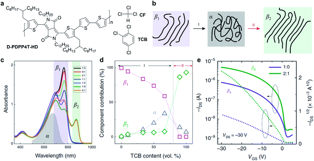 | ||
| Fig. 5 A new polymorphism of a DPP-based polymer induced by the solvent effect. (a) Chemical structures of D-PDPP4T-HD and chloroform (CF) and 1,2,4-trichlorobenzene (TCB). (b) Schematic diagram of the polymorphism transitions of D-PDPP4T-HD. (c) Absorption spectra of D-PDPP4T-HD in CF:TCB mixed solutions. The grey, purple, and green areas represent the absorption of the amorphous phase (α) in pure TCB at 100 °C, first (β1) and second (β2) ordered aggregated phases, respectively. (d) The contribution of the three solution-state aggregates in the mixed solutions. (e) Field-effect transistor performance of D-PDPP4T-HD in the β1 and β2 polymorphs obtained from the CF:TCB mixed solutions. Reproduced from ref. 89 with permission. Copyright 2019 Creative Commons Attribution 4.0. | ||
Using different ratios of o-dichlorobenzene (ODCB, a good solvent) and toluene (a poor solvent), Zheng et al. controlled the solution-state supramolecular assembly structures of a BDOPV-based conjugated polymer, and thus the electron mobility was boosted in the corresponding polymer thin-film FETs (Fig. 6).26 By adding 20% toluene into the ODCB solution, the spin-coated polymer films exhibited almost a doubly enhanced mobility of 3.24 cm2 V−1 s−1 and lowered activation energy barrier of 30 meV (Fig. 6b). When the proportion of toluene in the mixed solvent was further increased, the mobility gradually decreased. The difference in FET performance was attributed to the solution-state supramolecular assemblies in the mixed solution. SANS was employed to characterize the assembly structure in different solutions. SANS results showed that as the proportion of toluene increased, interactions between the polymer chains and the solvent molecules gradually decreased (Fig. 6c–e). In the good solvent ODCB, the polymer chains adopted extended backbones and exhibited one-dimensional (1D) worm-shaped assemblies (Fig. 6f), while in toluene, polymer chains adopted two-dimensional (2D) lamellar assemblies, dominated by the strong π–π interactions between conjugated backbones (Fig. 6g). When 20% toluene was added, the dimension of the solution-state supramolecular assembly structures underwent a transition from 1D to 2D structures (Fig. 6h). This work unraveled the important role of the solution-state assemblies or aggregates in obtaining the desired thin-film microstructures and improved FET performance.
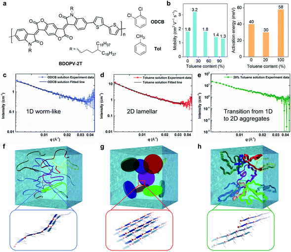 | ||
| Fig. 6 Solvent effect on solution-state aggregation and corresponding transistor performance of a BDOPV-based polymer. (a) Chemical structure of BDOPV-2T with toluene (Tol) and o-dichlorobenzene (ODCB). (b) Transistor mobility and charge transport activation energy evaluated from the polymer thin-films using the mixed solution. (c, d, e) Small angle neutron scattering (SANS) profiles and model-fitted curves of BDOPV-2T solution in ODCB, toluene, and 20% toluene/80% ODCB, respectively. (f, g, h) Schematic illustration of the proposed solution-state aggregates of BDOPV-2T in ODCB, toluene, and 20% toluene/80% ODCB, respectively. The possible chain packing in the 1D worm-like, 2D lamellar and dimension-transition aggregates is enlarged for clarity. Reproduced from ref. 26 with permission. Copyright 2017 WILEY-VCH. | ||
Apart from the solvent features, polymer solutions and crystallization temperatures are also critical to the polymer device performance.93 Yan and coworkers demonstrated high-performance thick-film polymer solar cells by forming a beneficial morphology, controlled by the temperature-dependent aggregation (TDA) of the donor polymers.94Via the TDA strategy, Yan and coworkers used environmentally friendly non-halogenated solvents and achieved efficient solar cells with power conversion efficiencies of up to 11.7%.23 Kim et al. reported a kinetically controlled crystallization of P(NDI2OD-T2), boosting the electron mobility up to 3.43 ± 0.39 cm2 V−1 s−1 in the P(NDI2OD-T2)-based thin-film FETs.95 The polymer solution was off-centre spin-coated onto the substrates and then crystallized under controlled temperatures. The kinetically controlled crystallization process produced large ordered domains in polymer thin films, benefiting the charge transport. Li et al. demonstrated the effect of dissolution temperature on polymer microstructures and FET performance.96 They found that the low dissolution temperature could generate extended polymer aggregation in solution and induced larger nanofibrils in the monolayer networks. Hence, the improved molecular ordering leads to a boosted mobility of 1 cm2 V−1 s−1.
Yao et al. systematically investigated the effect of temperature on controlling the solution-state aggregation, crystallization, and FET performance of conjugated polymers.40 The high temperature of the polymer solution during crystallization could promote the formation of the ordered solid-state microstructures and thereby improve the carrier transport in FETs (Fig. 7a). GIWAXS revealed that the film crystallized at 150 °C had more orderly stacked structures, while the film formed at a lower temperature is relatively more disordered (Fig. 7b). Solid-state microstructures of the thin films formed at different temperatures determine the difference in their FET properties. Films crystallized at 150 °C showed the highest electron mobility, which reached 3.7 cm2 V−1 s−1. The electron mobility was enhanced by two orders of magnitude compared to that of the film crystallized at 30 °C (Fig. 7c). To understand the crystallization process of conjugated polymers at different temperatures, they further studied the solution-state aggregates of conjugated polymers at different temperatures. In situ temperature-dependent absorption spectra showed that the interchain-related absorption peak decreased as the solution temperature increased. Meanwhile, in situ temperature-dependent SANS indicated that the size of solution-state polymer aggregates decreased. Further molecular simulations proved that the dihedral angle in the polymer backbone is prone to rotate at high temperatures, implying that the polymer conformation might be critical in solution-state aggregation. Besides, polymer chains experienced more intense thermal motion at higher temperatures, reducing the size of polymer aggregates. Therefore, at lower temperatures, the polymer formed larger aggregates in solution, in which the polymer chain packing was more disordered. The disordered structures in solution-state aggregates were incorporated into the deposited film, forming disordered packing microstructures. At higher temperatures, the thermal motion of molecules destroyed the original relatively disordered aggregated structures in solution. Breaking these disordered aggregated structures can help polymer chains form more ordered solid-state microstructures during the crystallization process.
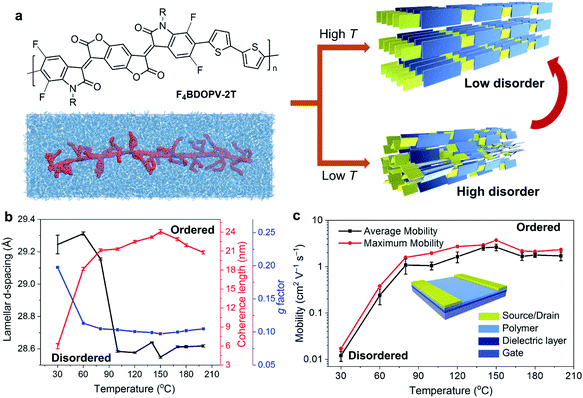 | ||
| Fig. 7 Enhanced transistor mobility and ordered solid-state microstructures of F4BDOPV-2T by controlling the solution-state aggregation and polymer crystallization. (a) Illustration of the ordered microstructures from the polymer solution using temperature-controlled aggregation. (b) Polymer packing distances and ordering parameters in thin-films deposited at different temperatures. (c) Transistor mobility, evaluated from the different polymer thin-films. Reproduced from ref. 40 with permission. Copyright 2020 WILEY-VCH. | ||
Polymer crystals and crystal structures
Single crystals and crystal structures of conjugated molecules and polymers are the ideal platforms for investigating the structure–property relationships.97,98 However, conjugated polymers usually crystalize with small grain sizes (about tens to hundreds of nanometres), making it quite difficult to obtain high-quality single crystals. Due to the lack of high-quality crystals, only a few instances of the crystal structures of conjugated polymers are reported. Therefore, it is an urgent necessity but with a significant challenge to acquire the crystal structures of conjugated polymers. With crystal structures, it becomes possible to truly understand the charge transport mechanism of conjugated polymers at molecular scales, hence accurate and precise molecular design rules can be established.Conjugated polymer crystals usually exhibited a long wire shape, called the nanowire or microwire, in previously reported studies. Um et al. reported the single-crystalline nanowires of a DPP-based polymer (Fig. 8a).99 They used a polymer batch of a low molecular weight of 8 kDa to grow the polymer nanowires, which exhibited high aspect ratios of 300 to 600. Selected-area electron diffraction (SAED) confirmed that the polymer backbone was aligned parallel to the long axis of the nanowires (Fig. 8b). Polymer nanowire FETs were successfully fabricated with a bottom gate/top contact configuration (Fig. 8c). The individual nanowire FET exhibited a remarkable hole mobility of up to 24 cm2 V−1 s−1 (Fig. 8d and e), which is the highest reported value in polymer crystal FETs.100 In addition, the polymer nanowire FETs showed high performance in photoresponsivity and photoswitching. Xiao et al. demonstrated a distinct variation of polymer orientation between two thiophene- and thiazole-containing DPP-based polymers in nanowire crystals (Fig. 8f).101 The minor structural change critically affected the polymer backbone orientations and the carrier mobilities in FETs. Polymers were prepared as a chloroform solution with 5 vol% ODCB for dissolution. Then, they obtained the polymer nanowires by dropping the diluted solution onto n-octyltrichlorosilane (OTS) modified Si/SiO2 substrates (Fig. 8g). SAED and GIWAXS results revealed that the thiophene-containing polymer adopted the edge-on packing motif but the thiazole-containing polymer adopted the face-on packing motif. Because of the ordered packing structures, the nanowires exhibited higher carrier mobilities compared to the thin-film devices (Fig. 8h).
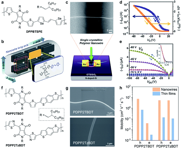 | ||
| Fig. 8 Nanowire field-effect transistors of DPP-based polymers. (a) Chemical structure of DPPBTSPE. (b) Polymer packing mode of DPPBTSPE in the nanowire crystals. (c) Schematic illustration and scanning electron microscopy (SEM) image of the nanowire field-effect transistor. (d) Transfer and (e) output curve of the DPPBTSPE nanowire transistor. Reproduced from ref. 99 with permission. Copyright 2015 American Chemical Society. (f) Chemical structures of PDPP2TBDT and PDPP2TzBDT. (g) SEM images of PDPP2TBDT and PDPP2TzBDT nanowires. (h) Comparison of the hole and electron mobility in the nanowires and thin-film transistors of PDPP2TBDT and PDPP2TzBDT. Reproduced from ref. 101 with permission. Copyright 2015 WILEY-VCH. | ||
Although crystals could be obtained in some example polymers, crystal structures of conjugated polymers have still not been generally realized. To acquire precise packing structures of conjugated polymers, scanning probe microscopies can provide meaningful images. Via high-resolution scanning tunneling microscopy (STM) and electrospray deposition, Costantini and coworkers established a direct approach to image both the individual and packed conjugated polymer chains.102 STM images were used to analyse the chemical defects in a DPP-based polymer as a model system. They pointed out that the interdigitation of alkyl side chains governs the backbone conformations in surface-adsorbed polymers. Using the same technique, Sirringhaus and coworkers demonstrated that rigid conjugated polymers with double bond connections employ an extended linear backbone structure.61 The rigid backbone allowed the formation of uniaxially aligned polymer films with a high electron mobility of 0.2 cm2 V−1 s−1, which was six times higher than the value measured in the unaligned films.60 Hence, the STM imaging technique is a powerful method for exploring the structure–property relationship of conjugated polymers in FETs.
Besides STM imaging, other indirect methods based on data fitting and rational assumptions are also practical to solve the crystal structures of conjugated polymers, including X-ray diffraction (XRD), electron diffraction, and molecular modelling (Fig. 9a). Hansen and coworkers revealed the crystal structure of P3HT.103 In their work, powder XRD and solid-state nuclear magnetic resonance (NMR) spectra provided the crystal lattice parameters and internuclear H–H distances (Fig. 9b). Through a controlled seeding approach, Reiter and coworkers obtained high-quality single crystals of P3HT.104 They built the crystal structures of P3HT with varied molecular weights, assisted by SAED analysis (Fig. 9c). The crystal structures of conjugated polymers are fundamentally regarded as a perfect platform and an initial model to study the structure–property relationship. For example, Venkateshvaran et al. used the crystal structures of IDTBT, poly(2,5-bis(3-alkylthiophen-2-yl)thieno(3,2-b)thiophene) (PBTTT), and P(NDI2OD-T2) to build their disordered and amorphous microstructures (Fig. 9d). The obtained microstructures supported their proposed concept of disorder-free charge transport in IDTBT-based polymer FETs.78
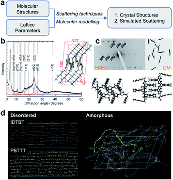 | ||
| Fig. 9 Structure elucidation of conjugated polymers. (a) Flow chart of structure elucidation. (b) Powder XRD profile and crystal structure of P3HT. Reproduced from ref. 103 with permission. Copyright 2012 WILEY-VCH. (c) SAED pattern, optical microscope (OM) image and P3HT single crystals. Reproduced from ref. 104 with permission. Copyright 2012 WILEY-VCH. (d) Disordered and amorphous microstructures of representative polymers starting from crystal structures. Reproduced from ref. 78 with permission. Copyright 2014 Nature Publishing Group. | ||
Summary and outlook
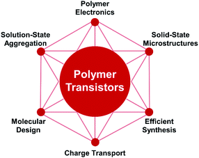
In this perspective, we have described in detail the recent developments in polymer field-effect transistors (Fig. 10). From the multi-level microstructures, we provide highlights of the molecular design, solution-state aggregation, and solid-state microstructures of conjugated polymers. These aspects are proven to be significant for obtaining high-performance polymer FETs. In addition, we further discuss the critical role of polymer crystals and crystal structures in understanding the in-depth charge transport of conjugated polymers. Several impressive approaches for determining the polymer packing structures are demonstrated, including direct imaging and indirect fitting methods. From the microcosmic understanding of the conjugated polymer microstructures, we consider that solution-state aggregation and its modulation will continuously attract more interest. The combination of multiple characterizations is urgently required to provide more structural information across several spatial scales. Hence, a clear relationship among molecular structures, solution-state aggregation, solid-state microstructures, and transistor performance needs to be established in the future.Furthermore, the development of high-performance polymer FETs requires not only molecular design and mechanism study but also practical applications in related functional devices. Addition of molecular additives, such as dopants, crosslinkers, and photosensitizers, is an effective method to solve the complications in practical applications, including large-scale fabrication,105,106 contact resistances,107 long-term stability,108,109 high-speed applications,110etc. For instance, contact doping by adding molecular dopants is one of the most used techniques to reduce contact resistance and improve transistor performance in both inorganic and organic FETs.111,112 Crosslinking the conjugated polymers makes the polymer thin film adequately robust for elaborate photopatterning to develop large-scale circuits.113,114 Mixing a photosensitizer or introducing porosity in polymer films causes significant environmental sensitivity in the case of polymer FETs.115,116 The device physics and facile fabrication of polymer FETs need more attention for large-scale fabrication of uniform high-performance FETs and sophisticated circuits.
In conclusion, controlling the solution-state aggregation and the solid-state microstructures will benefit the charge transport, leading to high-performance polymer FETs. The recent progress of polymer FETs will advance the future development of polymer electronics, including field-effect transistors, solar cells, electrochemical transistors, thermoelectrics, etc.
Conflicts of interest
There are no conflicts to declare.Acknowledgements
This work is supported by the National Key R&D Program of China (2017YFA0204701) and the National Natural Science Foundation of China (21420102005, 21790360, 21722201).Notes and references
- A. C. Arias, J. D. MacKenzie, I. McCulloch, J. Rivnay and A. Salleo, Chem. Rev., 2010, 110, 3–24 CrossRef CAS
.
- H. Sirringhaus, Adv. Mater., 2014, 26, 1319–1335 CrossRef CAS
.
- Z. Yi, S. Wang and Y. Liu, Adv. Mater., 2015, 27, 3589–3606 CrossRef CAS
.
- J. Yang, Z. Zhao, S. Wang, Y. Guo and Y. Liu, Chem, 2018, 4, 2748–2785 CAS
.
- H. Yan, Z. Chen, Y. Zheng, C. Newman, J. R. Quinn, F. Dötz, M. Kastler and A. Facchetti, Nature, 2009, 457, 679–686 CrossRef CAS
.
- H. Sirringhaus, P. J. Brown, R. H. Friend, M. M. Nielsen, K. Bechgaard, B. M. W. W. Langeveld-Voss, A. J. H. H. Spiering, R. A. J. J. Janssen, E. W. Meijer, P. Herwig and D. M. De Leeuw, Nature, 1999, 401, 685–688 CrossRef CAS
.
- F. Huang, Z. S. Bo, Y. H. Geng, X. H. Wang, L. X. Wang, Y. G. Ma, J. H. Hou, W. P. Hu, J. Pei, H. L. Dong, S. Wang, Z. Li, Z. G. Shuai, Y. F. Li and Y. Cao, Acta Polym. Sin., 2019, 50, 988–1046 Search PubMed
.
- A. D. Franklin, Science, 2015, 349, aab2750 CrossRef
.
- T. Someya, Z. Bao and G. G. Malliaras, Nature, 2016, 540, 379–385 CrossRef CAS
.
- C. Jiang, H. W. Choi, X. Cheng, H. Ma, D. Hasko and A. Nathan, Science, 2019, 363, 719–723 CrossRef CAS
.
- J. Zaumseil and H. Sirringhaus, Chem. Rev., 2007, 107, 1296–1323 CrossRef CAS
.
- H. H. Choi, K. Cho, C. D. Frisbie, H. Sirringhaus and V. Podzorov, Nat. Mater., 2018, 17, 2–7 CrossRef CAS
.
- A. F. Paterson, S. Singh, K. J. Fallon, T. Hodsden, Y. Han, B. C. Schroeder, H. Bronstein, M. Heeney, I. McCulloch and T. D. Anthopoulos, Adv. Mater., 2018, 30, 1801079 CrossRef
.
- A. Perinot and M. Caironi, Adv. Sci., 2019, 6, 1801566 CrossRef
.
- F. A. Viola, B. Brigante, P. Colpani, G. Dell'Erba, V. Mattoli, D. Natali and M. Caironi, Adv. Mater., 2020, 32, 2002329 CrossRef CAS
.
- C. B. Nielsen, M. Turbiez and I. McCulloch, Adv. Mater., 2013, 25, 1859–1880 CrossRef CAS
.
- X. Guo, A. Facchetti and T. J. Marks, Chem. Rev., 2014, 114, 8943–9021 CrossRef CAS
.
- C. Wang, H. Dong, W. Hu, Y. Liu and D. Zhu, Chem. Rev., 2012, 112, 2208–2267 CrossRef CAS
.
- H. Bronstein, C. B. Nielsen, B. C. Schroeder and I. McCulloch, Nat. Rev. Chem., 2020, 4, 66–77 CrossRef CAS
.
- Z.-D. Yu, Y. Lu, J.-Y. Wang and J. Pei, Chem.–Eur. J., 2020, 26, 16194–16205 CrossRef CAS
.
- H. Huang, L. Yang, A. Facchetti and T. J. Marks, Chem. Rev., 2017, 117, 10291–10318 CrossRef CAS
.
- P. Friederich, A. Fediai, S. Kaiser, M. Konrad, N. Jung and W. Wenzel, Adv. Mater., 2019, 31, 1808256 CrossRef
.
- J. Zhao, Y. Li, G. Yang, K. Jiang, H. Lin, H. Ade, W. Ma and H. Yan, Nat. Energy, 2016, 1, 15027 CrossRef CAS
.
- H. Hu, P. C. Y. Chow, G. Zhang, T. Ma, J. Liu, G. Yang and H. Yan, Acc. Chem. Res., 2017, 50, 2519–2528 CrossRef CAS
.
- R. S. Gurney, D. G. Lidzey and T. Wang, Rep. Prog. Phys., 2019, 82, 036601 CrossRef CAS
.
- Y.-Q. Zheng, Z.-F. Yao, T. Lei, J.-H. Dou, C.-Y. Yang, L. Zou, X. Meng, W. Ma, J.-Y. Wang and J. Pei, Adv. Mater., 2017, 29, 1701072 CrossRef
.
- M. M. Nahid, A. Welford, E. Gann, L. Thomsen, K. P. Sharma and C. R. McNeill, Adv. Electron. Mater., 2018, 4, 1700559 CrossRef
.
- V. Coropceanu, J. Cornil, D. A. da Silva Filho, Y. Olivier, R. Silbey and J.-L. Brédas, Chem. Rev., 2007, 107, 926–952 CrossRef CAS
.
- R. Noriega, J. Rivnay, K. Vandewal, F. P. V. Koch, N. Stingelin, P. Smith, M. F. Toney and A. Salleo, Nat. Mater., 2013, 12, 1038–1044 CrossRef CAS
.
- J. Rivnay, S. C. B. Mannsfeld, C. E. Miller, A. Salleo and M. F. Toney, Chem. Rev., 2012, 112, 5488–5519 CrossRef CAS
.
- S. Fratini, M. Nikolka, A. Salleo, G. Schweicher and H. Sirringhaus, Nat. Mater., 2020, 19, 491–502 CrossRef CAS
.
- N. M. Randell and T. L. Kelly, Chem. Rec., 2019, 19, 973–988 CrossRef CAS
.
- T. Lei, J.-Y. Wang and J. Pei, Chem. Mater., 2014, 26, 594–603 CrossRef CAS
.
- Z. Liu, G. Zhang and D. Zhang, Acc. Chem. Res., 2018, 51, 1422–1432 CrossRef CAS
.
- N. E. Jackson, B. M. Savoie, K. L. Kohlstedt, M. Olvera De La Cruz, G. C. Schatz, L. X. Chen and M. A. Ratner, J. Am. Chem. Soc., 2013, 135, 10475–10483 CrossRef CAS
.
- C. Sutton, C. Risko and J.-L. Brédas, Chem. Mater., 2016, 28, 3–16 CrossRef CAS
.
- J. P. Aime, F. Bargain, M. Schott, H. Eckhardt, G. G. Miller and R. L. Elsenbaumer, Phys. Rev. Lett., 1989, 62, 55–58 CrossRef CAS
.
- M. Grell, D. D. C. D. C. Bradley, X. Long, T. Chamberlain, M. Inbasekaran, E. P. P. Woo and M. Soliman, Acta Polym., 1998, 49, 439–444 CrossRef CAS
.
- R. Steyrleuthner, M. Schubert, I. Howard, B. Klaumünzer, K. Schilling, Z. Chen, P. Saalfrank, F. Laquai, A. Facchetti and D. Neher, J. Am. Chem. Soc., 2012, 134, 18303–18317 CrossRef CAS
.
- Z.-F. Yao, Z.-Y. Wang, H.-T. Wu, Y. Lu, Q.-Y. Li, L. Zou, J.-Y. Wang and J. Pei, Angew. Chem., Int. Ed., 2020, 59, 17467–17471 CrossRef CAS
.
- M. Li, C. An, T. Marszalek, M. Baumgarten, H. Yan, K. Müllen and W. Pisula, Adv. Mater., 2016, 28, 9430–9438 CrossRef CAS
.
- J. A. Lim, F. Liu, S. Ferdous, M. Muthukumar and A. L. Briseno, Mater. Today, 2010, 13, 14–24 CrossRef CAS
.
- Y. Olivier, D. Niedzialek, V. Lemaur, W. Pisula, K. Müllen, U. Koldemir, J. R. Reynolds, R. Lazzaroni, J. Cornil and D. Beljonne, Adv. Mater., 2014, 26, 2119–2136 CrossRef CAS
.
- H. Sun, X. Guo and A. Facchetti, Chem, 2020, 6, 1310–1326 CAS
.
- A. Tsumura, H. Koezuka and T. Ando, Appl. Phys. Lett., 1986, 49, 1210–1212 CrossRef CAS
.
- Z. Bao, A. Dodabalapur and A. J. Lovinger, Appl. Phys. Lett., 1996, 69, 4108–4110 CrossRef CAS
.
- J.-L. Brédas, Y. Li, H. Sun and C. Zhong, Adv. Theory Simul., 2018, 1, 1800016 CrossRef
.
- T. Körzdörfer and J.-L. Brédas, Acc. Chem. Res., 2014, 47, 3284–3291 CrossRef
.
- C. Adamo and D. Jacquemin, Chem. Soc. Rev., 2013, 42, 845–856 RSC
.
- J.-L. Bredas, Mater. Horiz., 2014, 1, 17–19 RSC
.
- K. Do, M. K. Ravva, T. Wang and J.-L. Brédas, Chem. Mater., 2017, 29, 346–354 CrossRef CAS
.
- B. Sun, W. Hong, Z. Yan, H. Aziz and Y. Li, Adv. Mater., 2014, 26, 2636–2642 CrossRef CAS
.
- W. Li, W. S. C. Roelofs, M. Turbiez, M. M. Wienk and R. A. J. Janssen, Adv. Mater., 2014, 26, 3304–3309 CrossRef CAS
.
- J. Ma, Z. Liu, J. Yao, Z. Wang, G. Zhang, X. Zhang and D. Zhang, Macromolecules, 2018, 51, 6003–6010 CrossRef CAS
.
- T. Lei, X. Xia, J.-Y. Y. Wang, C.-J. J. Liu and J. Pei, J. Am. Chem. Soc., 2014, 136, 2135–2141 CrossRef CAS
.
- J. Yang, Z. Zhao, H. Geng, C. Cheng, J. Chen, Y. Sun, L. Shi, Y. Yi, Z. Shuai, Y. Guo, S. Wang and Y. Liu, Adv. Mater., 2017, 29, 1702115 CrossRef
.
- Y. Gao, Y. Deng, H. Tian, J. Zhang, D. Yan, Y. Geng and F. Wang, Adv. Mater., 2017, 29, 1606217 CrossRef
.
- W. K. Chan, Y. Chen, Z. Peng and L. Yu, J. Am. Chem. Soc., 1993, 115, 11735–11743 CrossRef CAS
.
- X. Guo, R. P. Ortiz, Y. Zheng, Y. Hu, Y.-Y. Noh, K.-J. Baeg, A. Facchetti and T. J. Marks, J. Am. Chem. Soc., 2011, 133, 1405–1418 CrossRef CAS
.
- A. Onwubiko, W. Yue, C. Jellett, M. Xiao, H.-Y. Chen, M. K. Ravva, D. A. Hanifi, A.-C. Knall, B. Purushothaman, M. Nikolka, J.-C. Flores, A. Salleo, J.-L. Bredas, H. Sirringhaus, P. Hayoz and I. McCulloch, Nat. Commun., 2018, 9, 416 CrossRef
.
- M. Xiao, B. Kang, S. B. Lee, L. M. A. Perdigão, A. Luci, D. A. Warr, S. P. Senanayak, M. Nikolka, M. Statz, Y. Wu, A. Sadhanala, S. Schott, R. Carey, Q. Wang, M. Lee, C. Kim, A. Onwubiko, C. Jellett, H. Liao, W. Yue, K. Cho, G. Costantini, I. McCulloch and H. Sirringhaus, Adv. Mater., 2020, 32, 2000063 CrossRef CAS
.
- Y. Lu, Z.-D. Yu, R.-Z. Zhang, Z.-F. Yao, H.-Y. You, L. Jiang, H.-I. Un, B.-W. Dong, M. Xiong, J.-Y. Wang and J. Pei, Angew. Chem., Int. Ed., 2019, 58, 11390–11394 CrossRef CAS
.
- F. Zhang, Y. Hu, T. Schuettfort, C. Di, X. Gao, C. R. McNeill, L. Thomsen, S. C. B. Mannsfeld, W. Yuan, H. Sirringhaus and D. Zhu, J. Am. Chem. Soc., 2013, 135, 2338–2349 CrossRef CAS
.
- T. Lei, J.-H. Dou and J. Pei, Adv. Mater., 2012, 24, 6457–6461 CrossRef CAS
.
- J. Mei, D. H. Kim, A. L. Ayzner, M. F. Toney and Z. Bao, J. Am. Chem. Soc., 2011, 133, 20130–20133 CrossRef CAS
.
- J. Lee, A.-R. Han, H. Yu, T. J. Shin, C. Yang and J. H. Oh, J. Am. Chem. Soc., 2013, 135, 9540–9547 CrossRef CAS
.
- Y. Yang, Z. Liu, G. Zhang, X. Zhang and D. Zhang, Adv. Mater., 2019, 1903104 CrossRef CAS
.
- I. Kang, H.-J. Yun, D. S. Chung, S.-K. Kwon and Y.-H. Kim, J. Am. Chem. Soc., 2013, 135, 14896–14899 CrossRef CAS
.
- J.-H. Dou, Y.-Q. Zheng, T. Lei, S.-D. Zhang, Z. Wang, W.-B. Zhang, J.-Y. Wang and J. Pei, Adv. Funct. Mater., 2014, 24, 6270–6278 CrossRef CAS
.
- B. Kang, R. Kim, S. B. Lee, S.-K. Kwon, Y.-H. Kim and K. Cho, J. Am. Chem. Soc., 2016, 138, 3679–3686 CrossRef CAS
.
- C. Kanimozhi, N. Yaacobi-Gross, K. W. Chou, A. Amassian, T. D. Anthopoulos and S. Patil, J. Am. Chem. Soc., 2012, 134, 16532–16535 CrossRef CAS
.
- R. Kroon, D. Kiefer, D. Stegerer, L. Yu, M. Sommer and C. Müller, Adv. Mater., 2017, 29, 1700930 CrossRef
.
- J. Liu, L. Qiu, R. Alessandri, X. Qiu, G. Portale, J. Dong, W. Talsma, G. Ye, A. A. Sengrian, P. C. T. Souza, M. A. Loi, R. C. Chiechi, S. J. Marrink, J. C. Hummelen and L. J. A. Koster, Adv. Mater., 2018, 30, 1704630 CrossRef
.
- M. Moser, T. C. Hidalgo, J. Surgailis, J. Gladisch, S. Ghosh, R. Sheelamanthula, Q. Thiburce, A. Giovannitti, A. Salleo, N. Gasparini, A. Wadsworth, I. Zozoulenko, M. Berggren, E. Stavrinidou, S. Inal and I. McCulloch, Adv. Mater., 2020, 2002748 CrossRef CAS
.
- A. Giovannitti, C. B. Nielsen, D. T. Sbircea, S. Inal, M. Donahue, M. R. Niazi, D. A. Hanifi, A. Amassian, G. G. Malliaras, J. Rivnay and I. McCulloch, Nat. Commun., 2016, 7, 1–9 Search PubMed
.
- X. Zhang, H. Bronstein, A. J. Kronemeijer, J. Smith, Y. Kim, R. J. Kline, L. J. Richter, T. D. Anthopoulos, H. Sirringhaus, K. Song, M. Heeney, W. Zhang, I. McCulloch and D. M. DeLongchamp, Nat. Commun., 2013, 4, 2238 CrossRef
.
- W. Zhang, J. Smith, S. E. Watkins, R. Gysel, M. McGehee, A. Salleo, J. Kirkpatrick, S. Ashraf, T. Anthopoulos, M. Heeney and I. McCulloch, J. Am. Chem. Soc., 2010, 132, 11437–11439 CrossRef CAS
.
- D. Venkateshvaran, M. Nikolka, A. Sadhanala, V. Lemaur, M. Zelazny, M. Kepa, M. Hurhangee, A. J. Kronemeijer, V. Pecunia, I. Nasrallah, I. Romanov, K. Broch, I. McCulloch, D. Emin, Y. Olivier, J. Cornil, D. Beljonne and H. Sirringhaus, Nature, 2014, 515, 384–388 CrossRef CAS
.
- F. P. V. Koch, J. Rivnay, S. Foster, C. Müller, J. M. Downing, E. Buchaca-Domingo, P. Westacott, L. Yu, M. Yuan, M. Baklar, Z. Fei, C. Luscombe, M. A. McLachlan, M. Heeney, G. Rumbles, C. Silva, A. Salleo, J. Nelson, P. Smith and N. Stingelin, Prog. Polym. Sci., 2013, 38, 1978–1989 CrossRef CAS
.
- S. Himmelberger, K. Vandewal, Z. Fei, M. Heeney and A. Salleo, Macromolecules, 2014, 47, 7151–7157 CrossRef CAS
.
- A. S. M. Tripathi, S. Sadakata, R. K. Gupta, S. Nagamatsu, Y. Ando and S. S. Pandey, ACS Appl. Mater. Interfaces, 2019, 11, 28088–28095 CrossRef CAS
.
- D. Pei, Z. Wang, Z. Peng, J. Zhang, Y. Deng, Y. Han, L. Ye and Y. Geng, Macromolecules, 2020, 53, 4490–4500 CrossRef CAS
.
- Y.-Q. Zheng, T. Lei, J.-H. Dou, X. Xia, J.-Y. Wang, C.-J. Liu and J. Pei, Adv. Mater., 2016, 28, 7213–7219 CrossRef CAS
.
- J.-H. Dou, Y.-Q. Zheng, Z.-F. Yao, T. Lei, X. Shen, X.-Y. Luo, Z.-A. Yu, S.-D. Zhang, G. Han, Z. Wang, Y. Yi, J.-Y. Wang and J. Pei, Adv. Mater., 2015, 27, 8051–8055 CrossRef CAS
.
- K. C. Lim, C. R. Fincher and A. J. Heeger, Phys. Rev. Lett., 1983, 50, 1934–1937 CrossRef CAS
.
- B. McCulloch, V. Ho, M. Hoarfrost, C. Stanley, C. Do, W. T. Heller and R. A. Segalman, Macromolecules, 2013, 46, 1899–1907 CrossRef CAS
.
- Z. Fan, L. Zhang, D. Baumann, L. Mei, Y. Yao, X. Duan, Y. Shi, J. Huang, Y. Huang and X. Duan, Adv. Mater., 2019, 31, 1900608 CrossRef
.
- N. Hosono, A. Terashima, S. Kusaka, R. Matsuda and S. Kitagawa, Nat. Chem., 2019, 11, 109–116 CrossRef CAS
.
- M. Li, A. H. Balawi, P. J. Leenaers, L. Ning, G. H. L. L. Heintges, T. Marszalek, W. Pisula, M. M. Wienk, S. C. J. J. Meskers, Y. Yi, F. Laquai and R. A. J. J. Janssen, Nat. Commun., 2019, 10, 2867 CrossRef
.
- F. B. Dias, J. Morgado, A. L. Maçanita, F. P. Da Costa, H. D. Burrows and A. P. Monkman, Macromolecules, 2006, 39, 5854–5864 CrossRef CAS
.
- M. Knaapila, V. M. Garamus, F. B. Dias, L. Almásy, F. Galbrecht, A. Charas, J. Morgado, H. D. Burrows, U. Scherf and A. P. Monkman, Macromolecules, 2006, 39, 6505–6512 CrossRef CAS
.
- M. Knaapila and A. P. Monkman, Adv. Mater., 2013, 25, 1090–1108 CrossRef CAS
.
- B. Du, J. Yi, H. Yan and T. Wang, Chem.–Eur. J., 2020, 1–13 Search PubMed
.
- Y. Liu, J. Zhao, Z. Li, C. Mu, W. Ma, H. Hu, K. Jiang, H. Lin, H. Ade and H. Yan, Nat. Commun., 2014, 5, 5293 CrossRef CAS
.
- Y. Kim, N. Kim, W.-T. Park, C. Liu, Y.-Y. Noh and D.-Y. Kim, Adv. Funct. Mater., 2019, 29, 1807786 CrossRef
.
- M. Li, H. Bin, X. Jiao, M. M. Wienk, H. Yan and R. A. J. J. Janssen, Angew. Chem., Int. Ed., 2020, 59, 846–852 CrossRef CAS
.
- C. Wang, H. Dong, L. Jiang and W. Hu, Chem. Soc. Rev., 2018, 47, 422–500 RSC
.
- A. L. Briseno, S. C. B. Mannsfeld, S. A. Jenekhe, Z. Bao and Y. Xia, Mater. Today, 2008, 11, 38–47 CrossRef CAS
.
- H. A. Um, D. H. Lee, D. U. Heo, D. S. Yang, J. Shin, H. Baik, M. J. Cho and D. H. Choi, ACS Nano, 2015, 9, 5264–5274 CrossRef CAS
.
- X. Cao, K. Zhao, L. Chen, J. Liu and Y. Han, Polym. Cryst., 2019, 2, e10064 Search PubMed
.
- C. Xiao, G. Zhao, A. Zhang, W. Jiang, R. A. J. Janssen, W. Li, W. Hu and Z. Wang, Adv. Mater., 2015, 27, 4963–4968 CrossRef CAS
.
- D. A. Warr, L. M. A. Perdigão, H. Pinfold, J. Blohm, D. Stringer, A. Leventis, H. Bronstein, A. Troisi and G. Costantini, Sci. Adv., 2018, 4, eaas9543 CrossRef
.
- D. Dudenko, A. Kiersnowski, J. Shu, W. Pisula, D. Sebastiani, H. W. Spiess and M. R. Hansen, Angew. Chem., Int. Ed., 2012, 51, 11068–11072 CrossRef CAS
.
- K. Rahimi, I. Botiz, N. Stingelin, N. Kayunkid, M. Sommer, F. P. V. Koch, H. Nguyen, O. Coulembier, P. Dubois, M. Brinkmann and G. Reiter, Angew. Chem., Int. Ed., 2012, 51, 11131–11135 CrossRef CAS
.
- A. M. Zeidell, D. S. Filston, M. Waldrip, H. F. Iqbal, H. Chen, I. McCulloch and O. D. Jurchescu, Adv. Mater. Technol., 2020, 5, 2000390 CrossRef CAS
.
- Z.-F. Yao, Y.-Q. Zheng, Q.-Y. Li, T. Lei, S. Zhang, L. Zou, H.-Y. Liu, J.-H. Dou, Y. Lu, J.-Y. Wang, X. Gu and J. Pei, Adv. Mater., 2019, 31, 1806747 Search PubMed
.
- Y. Xu, H. Sun, A. Liu, H.-H. Zhu, W. Li, Y.-F. Lin and Y.-Y. Noh, Adv. Mater., 2018, 30, 1801830 CrossRef
.
- S. Park, S. H. Kim, H. H. Choi, B. Kang and K. Cho, Adv. Funct. Mater., 2020, 30, 1904590 CrossRef CAS
.
- E. K. Lee, M. Y. Lee, C. H. Park, H. R. Lee and J. H. Oh, Adv. Mater., 2017, 29, 1–29 Search PubMed
.
- H. Klauk, Adv. Electron. Mater., 2018, 4, 1700474 CrossRef
.
- O. Kwon, J. Y. Kim, S. Park, J. H. Lee, J. Ha, H. Park, H. R. Moon and J. Kim, Nat. Commun., 2019, 10, 3620 CrossRef
.
- A. F. Paterson, L. Tsetseris, R. Li, A. Basu, H. Faber, A. Emwas, J. Panidi, Z. Fei, M. R. Niazi, D. H. Anjum, M. Heeney and T. D. Anthopoulos, Adv. Mater., 2019, 31, 1900871 CrossRef
.
- M. J. Kim, M. Lee, H. Min, S. Kim, J. Yang, H. Kweon, W. Lee, D. H. Kim, J.-H. Choi, D. Y. Ryu, M. S. Kang, B. Kim and J. H. Cho, Nat. Commun., 2020, 11, 1520 CrossRef CAS
.
- H. W. Park, K. Choi, J. Shin, B. Kang, H. Hwang, S. Choi, A. Song, J. Kim, H. Kweon, S. Kim, K. Chung, B. Kim, K. Cho, S. Kwon, Y. Kim, M. S. Kang, H. Lee and D. H. Kim, Adv. Mater., 2019, 31, 1901400 CrossRef
.
- J. Ma, J. Tian, Z. Liu, D. Shi, X. Zhang, G. Zhang and D. Zhang, CCS Chem., 2020, 2, 632–641 CrossRef CAS
.
- X. Zhang, B. Wang, L. Huang, W. Huang, Z. Wang, W. Zhu, Y. Chen, Y. Mao, A. Facchetti and T. J. Marks, Sci. Adv., 2020, 6, eaaz1042 CrossRef CAS
.
| This journal is © The Royal Society of Chemistry 2021 |


