Two dimensional semiconducting polymers
Xin
Wei
a and
Mingfeng
Wang
 *ab
*ab
aSchool of Chemical and Biomedical Engineering, Nanyang Technological University, 62 Nanyang Dr, 637459, Singapore. E-mail: mfwang@ntu.edu.sg
bSchool of Science and Engineering, The Chinese University of Hong Kong, Shenzhen, Guangdong 518172, P. R. China
First published on 18th June 2020
Abstract
Two-dimensional semiconducting polymers (2DSPs) with planar π-conjugated structures have emerged as a new type of functional polymer material with unique chemical and physical properties. Their potential exciton migration and charge carrier transport in two dimensions are expected to bring new applications in optical, electrical, and sensing devices. In this review, we summarize recent synthetic strategies towards high-quality 2DSPs with controllable chemical structures, physical dimensions, and properties. We also discuss the perspectives of the potential applications of 2DSPs as advanced functional materials.
1. Introduction
The rapid advances in polymer science, engineering and industrialization of plastic products since Staudinger's vision of macromolecules in the 1930s have stimulated a paradigm shift of research since the 1950s to organic and/or polymeric materials with metallic properties, particularly electrical conductivity.1 Such materials are expected to combine the merits of the light-weight and potentially low cost of organic molecules, and mechanic flexibility of polymers, with the high electrical conductivity of conventional metals. One benchmark among them is tetrathiafulvalene (TTF) – 7,7,8,8,-tetracyanoquinodimethane (TCNQ), a type of complex made of a strong donor (D, TTF) and a strong acceptor (A, TCNQ) that form segregated D–A stacks in solid states. As a result, TTF–TCNQ is among the early examples of organic metals and superconductors discovered so far.2–5The discovery of polyacetylene and its remarkably enhanced electrical conductivity after iodine-oxidization by Shirakawa, Macdiarmid, and Heeger in 1977 has opened a new era of electrically conducting6,7 and semiconducting polymers8–18 with various chemical structures. To date, advances in molecular design and synthesis have led to a large variety of semiconducting molecules and polymers for high-performance devices such as light-emitting diodes (LEDs), field-effect transistors (FETs), photovoltaic devices, and sensors.19–34 Despite the enormous advances, the majority of the conducting and semiconducting polymers reported so far remained limited to one-dimensional (1D) linear chains composed of π-conjugated units along the backbones, which are appended with alkyl chains in many cases in order to improve the solubility in organic solvents and promote the solution-based processability.
The field of two-dimensional semiconducting polymers (2DSPs) has emerged recently, since the discovery of graphene, a two-dimensional atomic-layer-thin metal, from the mechanical exfoliation of graphite in 2004.35 Graphene has attracted intense research interest due to its compelling properties, including high mobility of charge carriers, high mechanical strength, and remarkably high thermal conductivity. A recent study by Cao et al. revealed the unconventional superconductivity of graphene superlattices.36
If one considers benzene as the “repeating unit”, then graphene is a covalently bond 2D π-conjugated polymer. Nevertheless, graphene is an intrinsic metallic material. Although graphene and its composites have shown great potential in a variety of applications where high electrical conductivity is desired, it shows limitations such as a low on/off ratio in semiconducting devices. There are basically two approaches to increasing the bandgap of graphene to convert it from a metal into a semiconductor. One is the “top-down” approach, by breaking its π-conjugation via either physical37 or chemical38,39 treatment. The other is the “bottom-up” approach, by the polymerization of rationally designed monomers with various structures and geometries. The latter has led to the development of a series of 2DSPs with controllable structures and chemophysical properties, as reviewed in detail in the following section.
2DSPs are expected to exhibit new optoelectronic properties as largely explored in 2D inorganic semiconducting materials such as transition metal dichalcogenides (TMDs).40–42 For instance, using both density functional theory (DFT) calculations and experimental approaches, Gutzler and Perepichka have demonstrated that the extended π-conjugation in 2DSPs leads to smaller band gaps compared to the 1D polymers composed of the same parent molecular repeat unit (Fig. 1a).43 With the aid of first-principles DFT, Ma and co-workers have also conducted a theoretical investigation of several representative 2DSPs and reported that the participation ratio (PR) of the frontier molecular orbital (either the highest occupied molecular orbital (HOMO) or the lowest unoccupied molecular orbital (LUMO)), corresponding to the delocalization length of π-conjugation, increases more rapidly in 2D polymers with the increase of the degree of polymerization (n), compared to 1D analogues composed of the same repeat units. Such a trend is noticeable when the π-conjugation between the adjacent repeat units is strong (Fig. 1b), but not so in weakly conjugated systems. Another intriguing prediction is a more significant charge oscillation amplitude in 2DSPs than that in 1D polymers, indicating that 2DSPs hold high potential in being unique non-linear optical materials (Fig. 1b).44 Other potential new properties of 2DSPs compared to 1D analogues remain to be explored both theoretically and experimentally.45,46
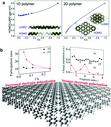 | ||
| Fig. 1 (a) Relationships between the highest occupied molecular orbital (HOMO)–lowest unoccupied molecular orbital (LUMO) gap and the degree of polymerization (n) for one-dimensional (1D) and 2D polymers. Reprinted with permission from ref. 43, Copyright 2013, American Chemical Society. (b) Evolution of participation ratio (corresponding to the delocalization length of π-conjugation) with a function of degree of polymerization (n), and charge population variation with fragment index, black dot: 1D polymers; red dot: 2D polymers. Reprinted with permission from ref. 44, Copyright 2016, American Chemical Society. | ||
In the present review, we highlight recent progress in the synthesis and characterization of 2DSPs. Section 2 presents the first three methods of interfacial polymerization as a “bottom-up” strategy to synthesize 2DSPs with high polymer integrity and controllable thickness. The fourth method by exfoliation from bulk-state layered polymers is presented in Section 3. We also discuss some perspectives and challenges facing the future advancement of this field. We note that the present review is not intended to be comprehensive by covering all of the reported works on the topic. In particular, 2D semiconducting metal–organic frameworks (MOFs), an interesting topic that has been covered in other excellent review articles,47,48 are not included.
2. Polymerization on the interface
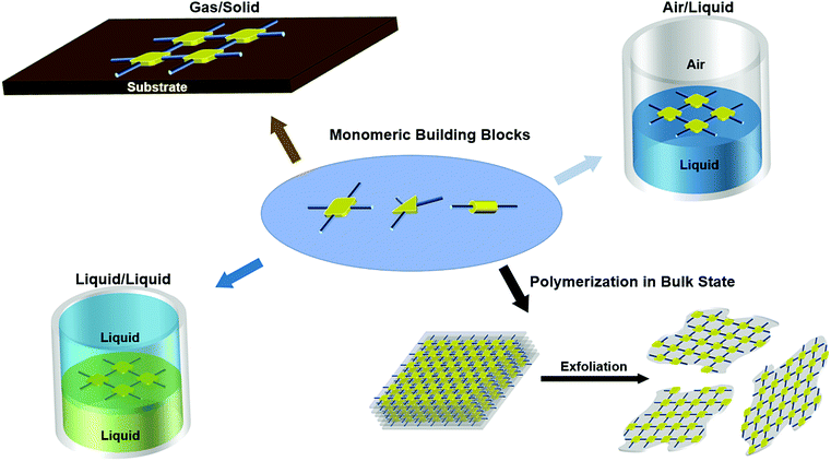
In this section, we highlight examples of three interfacial synthetic methods towards 2DSPs: polymerization on gas/solid, air/liquid, and liquid/liquid interfaces, respectively (Fig. 2). Each method is discussed in terms of monomer design, polymer size, thicknesses, crystalline polymorphs, and the presence of structural defects.Polymerization on the interface is a process when activated monomers react with each other to form 2D polymers on a flat interface between two different phases. Unlike the traditional solution-based reactions where monomers have full access to migrate in all three dimensions (x-, y-, and z-axis), polymerization on the interface offers a more restricted space (only x- and y-axis), leading to the formation of planar polymeric structures.
2.1 In situ polymerization on a gas/solid interface
Polymerization on gas/solid interfaces is typically conducted on a flat heating metal surface within the chamber of a scanning tunneling microscope (STM), and the chemistry involved was first inspired by Ullmann Coupling, a coupling reaction between aryl halides in the presence of copper catalysts.49 With the aid of the STM probe, the reaction process can be characterized at the molecular level.Grill et al. have summarized some key aspects of surface polymerization in their recent work.50 The choice of metal is critical because: (1) the metal surface serves as the catalyst for the reaction; (2) the molecular–surface interaction affects the reaction kinetics by governing the molecular mobility. Surface orientation plays an important role as well by inducing the preorganization of the activated monomer, resulting in the formation of the corresponding polymer configuration and the alignment of the intermediate and final polymers; and (3) reactivity and diffusion compete in the surface polymerization process. Whether it is a coupling-limited or diffusion-limited process depends on the molecular structure of the monomer.
Graphene nanoribbons (GNRs) are narrow strips of graphene, and they are believed to be semiconducting because of quantum confinement and edge effects.51 However, the production of high-quality GNRs with a width smaller than 10 nm remains a challenge.
The polymerization on a gas/solid surface has been reported by Müllen and co-workers to synthesize GNRs. The monomer they chose was 10,10′-dibromo-9,9′-bianthracene (M1) (Fig. 3a), and it had two bromine substituents. Those substituents were activated or dislocated at 200 °C, followed by the diffusion of dehalogenated intermediates and the formation of polymer chains through single covalent C–C bonds. The temperature was further increased to 400 °C in the following step, inducing an intermolecular cyclodehydrogenation within each polymer chain and transforming them into straight-edged GNRs (Fig. 3a). The formation of GNRs with good quality was in the corresponding STM image. A “zig-zag” GNR was made using the same method (Fig. 3c and d), proving the feasibility of this method, and more well-designed experiments could be conducted to investigate the properties of this emerging class of material.52
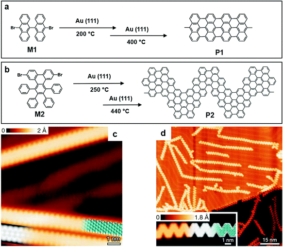 | ||
| Fig. 3 (a) Chemical structure of 10,10′-dibromo-9,9′-bianthracene (M1) and graphene nanoribbons (GNRs) formed by M1 (P1). (b) Chemical structure of 6,11-dibromo-1,2,3,4-tetraphenyltriphenylene (M2) and the GNRs formed by M2 (P2). (c) High-resolution (HR) STM image of P1. (d) HR-STM image of P2 and the corresponding ribbon length distribution. Reprinted with permission from ref. 52, Copyright 2010, Nature Publishing Group. | ||
2DSPs with larger dimensions than GNRs have been produced by polymerization on a gas/solid interface. In 2004, Grill et al. reported two different strategies of polymerization on top of a gold surface. The first strategy involved one monomer, tetra(4-bromophenyl) porphyrin (M3), which contains only one type of halogen substituent. It can undergo simultaneous and complete activation at 250 °C, and all four bromine substituents were lost simultaneously, resulting in the formation of a network of P3 (Fig. 4a and b). This method successfully proved that the topology of the nanostructure could be accurately crafted by controlling the chemical structure of the building blocks.53 In 2013, Perapichika and co-workers reported the same strategy on a silver plate with a different monomer, tetrabromotetrathienoanthracene (M4, Fig. 4e), which can be globally activated at 300 °C, creating the 2D conjugated polymer P4 (Fig. 4e). Similarly, the STM image of P4 proved the formation of 2DSP (Fig. 4f), as well as the electronic characterization on P4. Unexpectedly, the electronic gap of P4 was noticeably reduced despite the presence of observed misconnection defects. Compared with the 1D polymer formed by M4, the π-conjugation in the 2DSP form was reported to be more efficient due to the more significant amount of orbital overlapping between the monomers.54
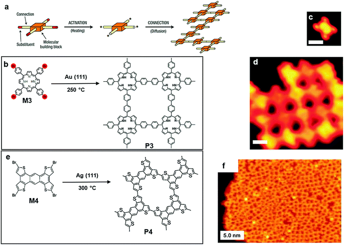 | ||
| Fig. 4 (a) Schematic illustration of polymerization (one step) onto the solid surfaces of Au(111) (a–d) or Ag(111) (e–f). (b) Chemical structure of tetra(4-bromophenyl)porphyrin (Br4TPP) (M3) and polymer3 (P3). (c) STM image of M3 (scale bar 1 nm). (d) STM image of P3 (scale bar 5 nm). Reprinted with permission from ref. 53, Copyright 2007, The Nature Nanotechnology. (e) Chemical structure of tetrabromotetrathienoanthracene (TBBTA) (M2) and nanostructure polymer 4 (P4). (f) STM image of P4 (scale bar 5 nm). Reprinted with permission from ref. 54, Copyright 2013, The Royal Society of Chemistry. | ||
The second strategy reported by Grill et al. involved a different type of molecular precursor, 5,15-bis(4-bromophenyl)-10,20-bis(4-iodophenyl)porphyrin (M5) (Fig. 5a and b), with two kinds of halogen substituents bound to the phenyl groups alternatively. Because of different reactivities of those two kinds of substituents, M5 can undergo sequential activations: the iodine substituents were activated at a temperature of 120 °C, and a linear polymer chain was formed owing to the trans-configuration of the building block. The STM image shows clear evidence for this step (Fig. 5c). Afterwards, the brominated monomers were activated by increasing the amount of thermal energy provided. Polymer chains with activation spots joined together to build a 2D network. As shown in the corresponding STM image (Fig. 5d), a well-defined 2DSP was produced, proving that control over reactivity and diffusion during the formation of covalent bonds is an effective route towards the creation of well-defined nanostructures.55
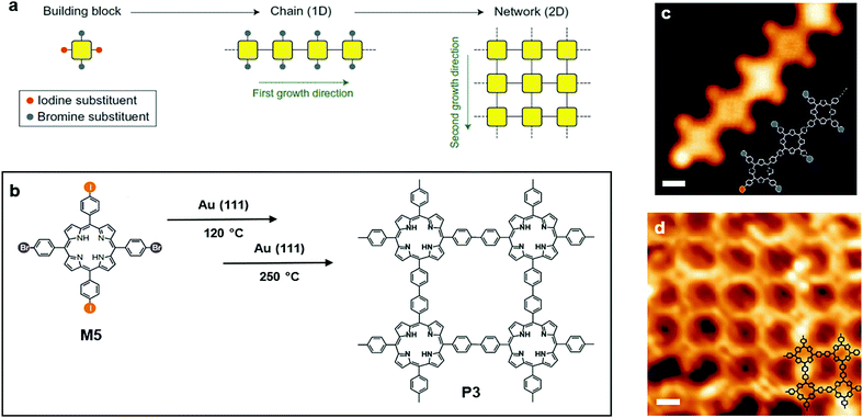 | ||
| Fig. 5 (a) Schematic illustration of polymerization (two steps) onto the solid surface of Au(111). (b) Chemical structure of 5,15-bis(4-bromophenyl)-10,20-bis(4-iodophenyl)porphyrin (trans-Br2I2TPP) (M5) and polymer3 (P3). (c) STM image of the chain formed by M5 (scale bar 1 nm). (d) STM image of P3 (scale bar 1 nm). Reprinted with permission from ref. 55, Copyright 2012, Nature Publishing Group. | ||
Though in situ polymerization on a gas/solid interface has led to well-defined 2DSPs, it is still challenging to produce wafer-size 2DSPs with minimal defects. One possible solution given by Müllen et al. was the adaption of the transfer methods developed for epitaxial graphene. It involved a simple ‘chip-to-chip press’ method, and the preliminary results suggested that unbroken GNR pieces could be successfully transferred from a gold surface onto a SiO2 substrate.52,56
2.2 Polymerization on a air/liquid interface
This type of polymerization happens typically at the interface of air and water in a Langmuir–Blodgett trough. The movable barriers of the trough provide confinement, which assists in the formation of a 2D structure. An electro-balance probe sticking into the water minimizes the effect of the electrostatic interaction between the nanostructure and the Wilhelmy plate. It is achievable to produce large size single layer or multiple layer 2D nanostructures using traditional air/liquid polymerization. However, it is still largely demanding to maximize the size of crystallinity, a key aspect affecting the charge transport property of 2DSPs.Feng and co-workers reported their solution to address the problem using a surfactant-monolayer-assisted interfacial synthesis (SMAIS) method (Fig. 6a). The surfactant they chose was sodium oleyl sulfate (SOS) (Fig. 6a), which was dissolved in an organic solvent such as chloroform and then spread onto the water phase. Upon the complete evaporation of chloroform, the long-chain of SOS assisted the assembly into a well-organized monolayer with the polar heads facing the water phase. Afterward, 5,10,15,20-tetrakis(4-aminophenyl)porphyrin (M6) was protonated by hydrogen chloride followed by injection into the water phase. M6 was absorbed by the SOS polar heads by hydrogen bonding and electrostatic interaction. The last step was the addition of 2,5-dihydroxyterephthalaldehyde (M7), resulting in the formation of covalent bonds through a condensation reaction of aldehyde and amine groups (Fig. 6b). Eventually, a wafer size 2DSP was obtained (Fig. 6c). Furthermore, they added a Lewis acid metal triflate catalyst Yb(OTf)3 which effectively catalysed the imine formation into the water phase. The average single-crystalline domain of P5 reached ca. 150 nm, as clearly shown by the high-resolution TEM image (Fig. 6d). Interestingly, the thickness of 2DSP can be altered by only changing the concentrations of M6 and M7, without compromising the crystallinity. The photoconductive properties of P5 were studied using time-resolved terahertz spectroscopy, and a thin film of P5 with a thickness of 20 nm demonstrated a p-type semiconducting behaviour with a bandgap of 1.38 eV and a hole mobility of 0.01 cm2 V−1 s−1.57 The impressively large-size single-crystalline domain makes this method a promising pathway to monolayer 2DSP.
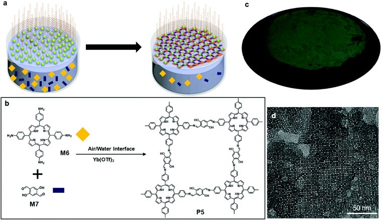 | ||
| Fig. 6 (a) Schematic illustration of polymerization at the air–water interface; a representative of SOS is highlighted with the red box. (b) Chemical structure of 5,10,15,20-tetrakis(4-aminophenyl)porphyrin (M6), 2,5-dihydroxyterephthalaldehyde (M7), and polymer 5 (P5). (c) Digital picture of monolayer P5 on 4 inch 300 nm SiO2/Si wafer. (d) TEM image of monolayer P5 (scale bar 50 nm). Reprinted with permission from ref. 57, Copyright 2020, Angewandte Chemie. | ||
Wang and co-workers reported the preparation of 2D π-conjugated supramolecular polymers as a thin film state on the air/water interface. The monomer, 3,6-bis(4-((2-octyldodecyl)oxy)phenyl)-2,5-dihydropyrrolo[3,4-c]pyrrole-1,4-dione (M8), is composed of a rigid and planar core of phenyl-flanked diketopyrrolopyrrole and “soft” branched alkoxy chains that enhance the solubility in a variety of organic solvents (Fig. 7a and b). The sizeable thin film formed by the self-assembly of M8 was transparent and uniform and can be easily transferred onto glass substrates, which showed very weak fluorescence under UV light of 365 nm (Fig. 7c and d). The formation of the supramolecular polymers as thin films was reflected using UV-vis absorption spectroscopy: a strong absorption band at 534 nm and a shoulder vibronic transition at 495 nm. The TEM image of P6 constructed from the air/water interface clearly showed that the film was smooth and uniform (Fig. 7f).58 An open issue in this supramolecular 2D π-conjugated system is to examine the charge transport within the π-conjugated layer and how the π–π stacking and H-bonding determine the charge carrier mobility and anisotropic feature of the charge transport.
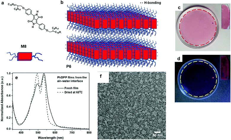 | ||
| Fig. 7 (a) Chemical structure of 3,6-bis(4-((2-octyldodecyl)oxy)phenyl)-2,5-dihydropyrrolo[3,4-c]pyrrole-1,4-dione (M8). (b) Schematic illustration for 2D aggregation driven by both hydrogen bonding (H-bonding) and π–π stackings (Lamellar phase) (P6). (c) Digital photograph of M8 films prepared at the air/water interface under visible light. Inset: digital photograph of films transferred on glass slides. (d) Digital photograph of M8 films prepared on the air/water interface under UV (365 nm) light. Inset: digital photograph of films transferred on glass slides. (e) UV-vis absorption spectra of fresh films (solid line) and films dried at 60 °C (dashed line). (f) TEM image of P6 (scale bar 50 nm). Reprinted with permission from ref. 58, Copyright 2019, American Chemical Society. | ||
Compared with polymerization on a gas/solid interface, the air/liquid interfacial polymerization is more favorable because: (1) it does not require high-cost equipment; (2) it does not require an elegant metal catalyst with the specific surface configuration; and (3) the reaction can be carried out under relatively mild conditions and is amenable to scale up.
2.3 Polymerization on a liquid/liquid interface
Polymerization on a liquid/liquid interface is very similar to that on the air/liquid interface. The second layer of liquid, which is typically organic and immiscible with the aqueous phase, provides a large variety of monomer or catalyst choices, which could be insoluble in the aqueous phase.In 2016, Sahabudeen et al. reported the synthesis of 2DSP P5 and P5′ using polymerization on the liquid/liquid interface (Fig. 8a). M6 or M6′, a porphyrin monomer with cobalt, and M7 were dissolved into chloroform and water, respectively, and the Schiff-base polycondensation happened at the interface. The system was left undisturbed for ten days, and multiple layer P5 or P5′ was fished out onto a 4-inch SiO2/Si wafer (Fig. 8c). P5 produced with this method was multilayer, and it was clearly shown in the TEM image (Fig. 8d). In contrast to multi-layered structures of P5 obtained from the liquid/liquid interfacial polymerization, when P5 was synthesized by polymerization on the air/water interface in a Langmuir–Blodgett trough, a monolayer 2DSP was obtained. This monolayer P5 had an average Young's modulus of EYoung = 267 ± 30 GPa, which was comparable to some other 2D materials such as graphene (EYoung = 1 TPa) and graphene oxide (EYoung = 208 GPa). More interestingly, this cobalt modified multilayer P5′ showed a catalytical effect in the hydrogen generation from water splitting.59
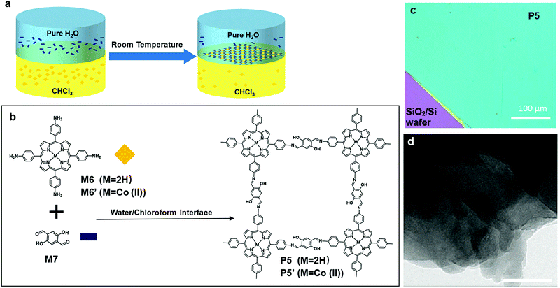 | ||
| Fig. 8 (a) Schematic illustration of polymerization at the chloroform–water interface. (b) Chemical structure of 5,10,15,20-tetrakis(4-aminophenyl) (M6 (M = 2H); M6′ (M = Co(II))), 2,5-dihydroxyterephthalaldehyde (M7), and polymer 5′ (P5 (M = 2H); P5′ (M = Co(II))). (c) Digital picture of multilayer P5 on 4 inch 300 nm SiO2/Si wafer (scale bar 100 μm). (d) TEM of multilayer P5 (scale bar 50 nm). Reprinted with permission from ref. 59, Copyright 2016, Nature Publishing Group. | ||
In 2017, Matsuoka and co-workers successfully synthesized graphydiyne (P7) by carbon–carbon bond formation at the liquid/liquid interface. Unlike P5 or P5′, there is only one type of monomer needed for P7 (Fig. 9a and b), hexaethynylbenzene (M9). M9 was dissolved into dichloromethane (DCM), while the aqueous phase contained the copper(II) acetate catalyst. The system was kept under an argon atmosphere for 24 hours, allowing the formation of multiple layer P7 at the liquid/liquid interface. The HR-TEM image showed the lattice fringes of P7 with an interval of 0.82 nm (Fig. 9c).60
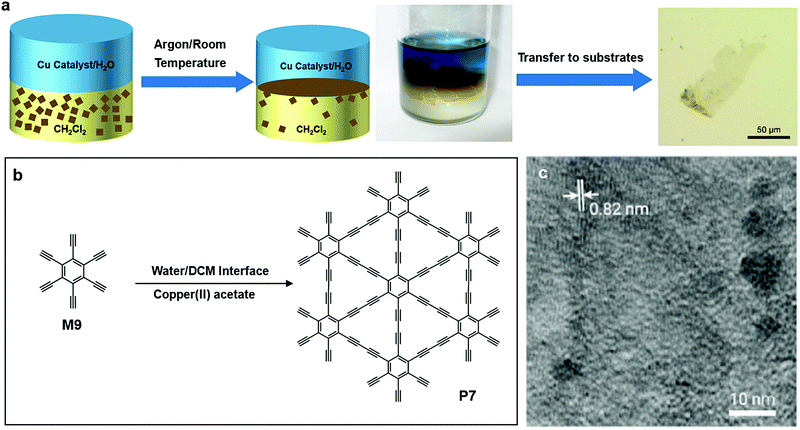 | ||
| Fig. 9 (a) Schematic illustration of polymerization at the DCM–water interface. (b) Chemical structure of hexaethynylbenzene (M9) and (c) chemical structure of graphydiyne (P7). (d) HR-TEM image of P7 (scale bar 500 nm). Reprinted with permission from ref. 60, Copyright 2017, American Chemical Society. | ||
Recently, Li and co-workers reported porous P8via Suzuki polymerization on a water/toluene interface at 2 °C for one month (Fig. 10a and b). After the reaction, P8 was transferred onto a glass substrate and washed with various organic and inorganic solvents to remove unreacted monomers. They embedded P8 thin film into a field-effect transistor (FET) and observed a charge carrier mobility of 3.2 × 10⁻³ cm2 V−1 s−1. Moreover, P8 showed a good catalytic effect on the hydrogen evolution reaction. Under the same reaction conditions (Fig. 10c), another polymer P9 formed by the liquid/liquid interfacial polymerization of a porphyrin monomer M12 and M13 could be vividly observed at the interface (Fig. 10d and e).61
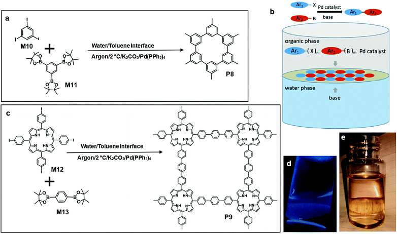 | ||
| Fig. 10 (a) Chemical structure of tris(4,4,5,5-tetramethyl-1,3,2-dioxaborolan-2-yl)benzene (M10), triiodobenzene (M11) and polymer 8 (P8). (b) Schematic illustration of polymerization at the toluene–water interface, Suzuki reaction between the aryl groups. (b) Synthesizing 2D-COF on the interface by Suzuki polymerization (Ar = aryl group; X = halide; B = boronic group; m, n + 2 and at least one + 3). (c) Chemical structure of 5,10,15,25-tetrakis(4-iodophenyl) porphyrin (M12), 1,4-benzene diboronic acid dipinacol ester (M13) and polymer 9 (P9). (d) Fluorescence photograph of P8 at the interface under UV light (365 nm) P8. (e) Digital photograph of P9 under visible light. Reprinted with permission from ref. 61, Copyright 2019, Angewandte Chemie. | ||
So far, the overall quality of 2DSPs formed by polymerization at the liquid/liquid interface does not appear as good as those from the air/liquid interface. Further optimization of the liquid/liquid interfacial polymerization is needed in the future to improve the reaction kinetics and efficiency under ambient temperature and pressure, as well as the crystalline ordering in a large size scale.
3. Exfoliation from layered bulk polymers
The fourth method of synthesizing 2DSPs as discussed in this section represents a “top-down” approach by exfoliation from bulk polymers, which are often π-conjugated covalent organic frameworks (COFs) with 3D exfoliable layered structures. This method, similar to the exfoliation of graphite and some layered TMDs, is becoming increasingly attractive because of its versatility, ease to scale up, and being achievable using equipment and chemicals available in normal chemical laboratories (Fig. 2).Jiang and co-workers reported a type of stable sp2 COF (P10), which retains the crystallinity, porosity, and luminescent properties even after one year of exposure in air. The polycondensation between M14 and M15 results in the predesigned tetragonal sp2 carbon lattices, which are π conjugated along both the x and y directions. The lattice had a designed pore size of 1.9 nm, and the pore size distribution calculated from non-linear density functional theory showed that only one type of pore was present in P10 (Fig. 11a). Moreover, the resulting frameworks with tuneable band gaps can be exfoliated into nanosheets. The HR-TEM image of P10 clearly showed that the pore size was 1.9 nm as expected.62
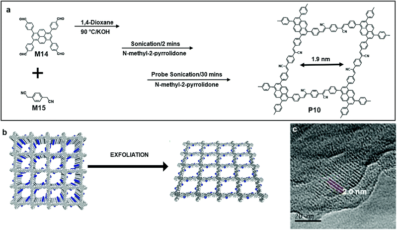 | ||
| Fig. 11 (a) Chemical structure of 1,3,6,8-tetrakis(4-formylphenyl)pyrene (M14), 2,2′-(1,4-phenylene)diacetonitrile (M15) and polymer 8 (P10). (b) Schematic illustration of exfoliation from layered bulk polymers. (c) HRTEM image of an exfoliated single layer of P10 (scale bar 20 nm). Reprinted with permission from ref. 62, Copyright 2018, Nature Publishing Group. | ||
Perepichka's group recently reported the synthesis of a series of (aza)triangulate based COFs (P11). The monomer precursor, 4,4′,4′′-trinitro-2,2′:6′,2′′:6′′,6-trioxytriphenylamine, was hydrogenated by a Pd catalyst into M16. At the same spot, polycondensation between the amine groups from M16 and the aldehyde groups from M7 occurred (Fig. 11a), followed by the exfoliation of the layered bulk polymer into nanosheet by ultrasonication for 5 minutes. The 2DSPs were in multilayer states, and the porous structure of each layer was not directly observed in the TEM image (Fig. 12a and b). After being doped with iodine, the optical extinction absorption of P11 became broad and spanned into the mid-IR region (<0.2 eV), which proved the semiconducting property of P11. Moreover, they found that doped P11 showed a paramagnetic property under cryogenic conditions.63
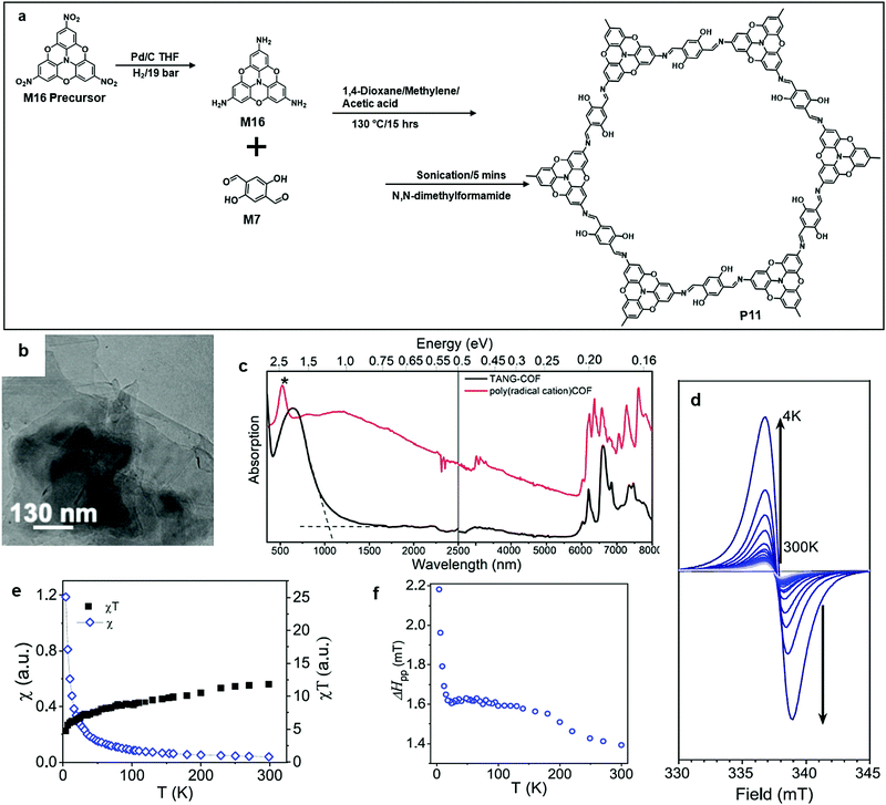 | ||
| Fig. 12 (a) Chemical structure of 4,4′,4′′-trinitro-2,2′:6′,2′′:6′′,6-trioxytriphenylamine, 4,4′,4′′′-triamino-2,2′:6′,2′′:6′′,6-trioxytriphenylamine (M16), and polymer 11 (P11). (b) TEM image of P11 (scale bar 130 nm). (c) Optical extinction spectra for P11 (black, KBr pellet) and iodine-doped P11 (red, Nujol suspension). (d) ESR spectra of iodine-doped P11 at different temperatures. (e and f) Temperature dependence of (e) the spin susceptibility and (f) the ESR line width. Reprinted with permission from ref. 63, Copyright 2020, American Chemical Society. | ||
Triazine-containing conjugated polymers have been promising for versatile applications due to their nitrogen-rich optoelectronic nature. The traditional synthetic methods require the monomers to bear a high temperature or strong acid treatment, which limits the choices of monomers. Hence, a more appropriate strategy with milder reaction conditions is increasingly attractive.
Perepichka's group reported that the aldol condensation of trimethyltriazines (M17) with aromatic dialdehydes (M18) was an efficient synthetic pathway towards a crystalline poly (arylene vinylene)s COF (P12) (Fig. 13a). P12 was extremely thermally stable, and it survived from thermal treatment up to 400 °C. Meanwhile, it was highly chemically inert. Interestingly, crystalline P12 pellets only swelled when treated with protonic solvents such as water and methanol (Fig. 13c). This could be attributed to the hydrogen bonding formed between immersed water molecules and triazine nitrogen atoms. As a result, there was a small expansion of both in-plane polymer periodicity and interlayer stacking distance. Powder X-ray diffraction (PXRD) was used to determine the material structural characteristics of a powder sample, and the PXRD result of water-swelled COF-1 shows a significant increase in the intensities of (h0) relative to (h00) (Fig. 13d). Lastly, P12 is highly fluorescent and the colour of the emission red-shifted with the increase of the solvent polarity (Fig. 13e).64
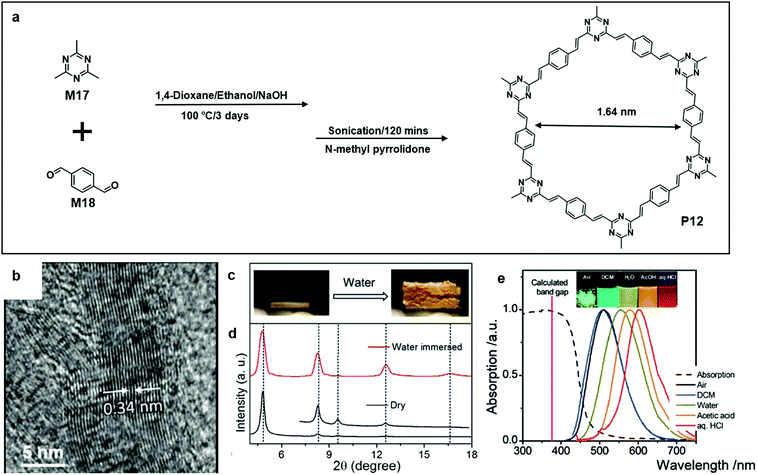 | ||
| Fig. 13 (a) Chemical structure of 2,4,6-trimethyl-1,3,5-triazine (M17), terephthalaldehyde (M18), and polymer 11 (P12). (b) HR-TEM image of an exfoliated single layer of P10 (scale bar 5 nm). (c) Photograph showing the swelling effect on dry P12 pellets; before adding water drops (left) and after adding water drops (right). (d) Comparison of PXRD patterns of dry and water immersed COF. (e) Absorption (dashed line) and photoluminescence (solid line, λex = 430 nm) spectra of P12 in the solid-state and dispersed in solvents with different polarities. Inset: photograph of the COFs in the different environments under 365 nm illumination. Reprinted with permission from ref. 64, Copyright 2019, Angewandte Chemie. | ||
In 2017, Liu et al. reported the synthesis of a crystalline single-layer or few-layer triazine-based COF (P13) with the trimerization of carbonitriles in the liquid phase followed by 10 minutes of sonication (Fig. 14a and b). P13 has a predicted pore size of 1.4 nm based on the density functional based tight-binding (DFTB) calculations. The prediction was evident in the corresponding HR-TEM image (Fig. 14c and d). A piece of free-standing P13 film showed greenish-blue fluorescence under UV light irradiation (Fig. 14f). Furthermore, a FET device involving the P13 film functioning as the semiconducting layer showed an ambipolar charge transport with a mobility of 0.15 cm2 V−1 s−1 and a moderate on/off ratio of 1200.65
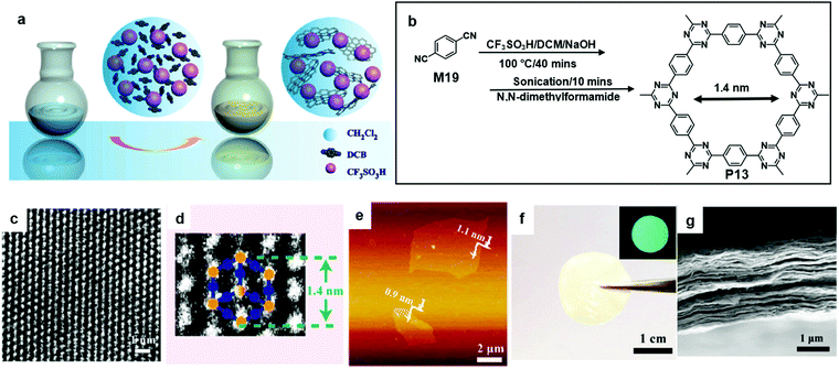 | ||
| Fig. 14 (a) Schematic illustration of polymerization with the aid of CF3SO3H. (b) Chemical structure of 1,4-dicyanobenzene (M19) and polymer 12 (P13). (c) Higher-magnification HR-TEM image of P13. (d) HR-TEM image of P13. (e) AFM images of single layer P13. (f) Photograph of the free-standing 2DP film with the inset showing its fluorescent image under UV light. (g) Cross-sectional SEM images of the 2COF film (scale bar 1 μm). Reprinted with permission from ref. 65, Copyright 2017, American Chemical Society. | ||
Recently, Wang and co-workers reported the synthesis of triazine-based 2D conjugated porous polymers through direct arylation polymerization, a facile, atom-efficient, and environmentally benign pathway. A library of π-conjugated polymers P14–16 was successfully produced (Fig. 15a), using commercially available aryl bromide monomers M21–23.19,66–68 The photocatalytic activity for the oxidation of benzylamine was characterized. Specifically, P16 showed an outstanding performance and excellent reusability, and an 80% conversion was obtained even after the 5th cycle of the experiment. The TEM images showed that the polymers were in layer structures (Fig. 15b–d).69 They also demonstrated the synthesis of few-layered 2DSPs by the direct arylation polymerization of M22 with M24 containing diketopyrrolopyrrole (DPP) moieties (Fig. 16a). The exfoliation of the bulk-state polymers in o-dichlorobenzene at 120 °C resulted in thin-layered 2DSPs that could be directly visualized under high-resolution TEM imaging (Fig. 16b).70 The results suggest that the branched alkyl chains attached to the DPP building blocks benefit the exfoliation of P17 in the solvent. But the impact of such bulky alkyl chains on the charge transport of such 2DSPs in devices remains to be studied in the future.
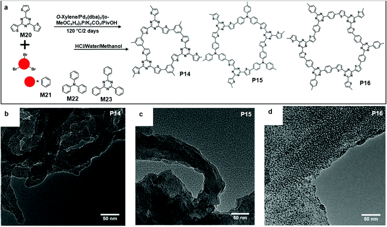 | ||
| Fig. 15 (a) Chemical structure of 2,4,6-(tri-2-thienyl)-1,3,5-Triazine (M20), 1,3,5-tribromobenzene (M21), tris(4-bromophenyl)amine (M22), 2,4,6-tris(4-bromophenyl)-1,3,5-triazine (M23), and polymer 14 (P14), polymer 15 (P15), and polymer 16 (P16). (b) TEM image of P14 (scale bar 50 nm). (c) TEM image of P15 (scale bar 50 nm). (d) TEM image of P16 (scale bar 50 nm). Reprinted with permission from ref. 66, Copyright 2018, The Royal Society of Chemistry. | ||
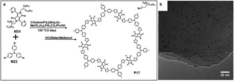 | ||
| Fig. 16 (a) Chemical structure of 2,5-bis(2-octyldodecyl)-3,6-di(thiophen-2-yl)-2,5-pyrrolo[3,4-c]pyrrole-1,4(2H,5H)-dione (M24) and polymer 22 (P22). (b) TEM image of P17 (scale bar 25 nm). Reprinted with permission from ref. 67, Copyright 2017, American Chemical Society. | ||
The ease to scale up and relatively low cost are the advantages of the present method of exfoliating layered bulk polymers. The quality of the resulting 2DSPs could be sufficient for some applications such as photocatalysis. Further improvements of the structural ordering with minimal defects over a large size scale and applications of these polymers for high-performance semiconductor devices need to be addressed in the future.
4. Conclusion
In summary, we have reviewed the major synthetic methods towards a variety of 2DSPs with tunable molecular structures, physical dimensions and chemophysical properties. Although some monolayer or multilayer 2DSPs with controllable sizes and thicknesses have been obtained using synthetic strategies of interfacial polymerization or exfoliation of bulk layered polymers, certain challenges remain to be addressed to realize the potential of 2DSPs for a variety of applications. For instance, how can the crystalline phase and grain sizes be controlled so that the overall quality of 2DSPs can be improved? Another issue is how to transfer the pre-formed 2DSPs onto a substrate such as SiO2/Si wafer with minimal impact on the structural integrity of 2DSPs. Thus, more efforts are required to explore efficient reactions and develop specific building blocks with desired properties.The extended conjugation in the second dimension imparts 2DSPs with reduced band gaps and enhanced charge delocalization compared with the 1D analogues, while other potentially intriguing properties such as excitonic coupling and quantum effect remain to be discovered in the future. We forsee that 2DSPs could become a new generation of organic and polymeric 2D materials with multifunctional properties for advanced applications such as high-performance optoelectronic devices, sensors, catalysis and spintronic devices.71–74
Conflicts of interest
There are no conflicts to declare.Acknowledgements
M. W. is thankful for the financial support by AcRF Tier 1 (2016-T1-001-214; 2018-T1-001-173) from the Ministry of Education, Singapore. X. W. is thankful for the financial support of a PhD scholarship from Nanyang Technological University.Notes and references
- F. Wudl, Spiers Memorial Lecture Organic electronics: an organic materials perspective, Faraday Discuss., 2014, 174(0), 9 RSC.
- H. Alves, A. S. Molinari, H. Xie and A. F. Morpurgo, Metallic conduction at organic charge-transfer interfaces, Nat. Mater., 2008, 7(7), 574 CrossRef CAS PubMed.
- M. Bendikov, F. Wudl and D. F. Perepichka, Tetrathiafulvalenes, Oligoacenenes, and Their Buckminsterfullerene Derivatives:
![[thin space (1/6-em)]](https://www.rsc.org/images/entities/char_2009.gif) The Brick and Mortar of Organic Electronics, Chem. Rev., 2004, 104(11), 4891 CrossRef CAS PubMed.
The Brick and Mortar of Organic Electronics, Chem. Rev., 2004, 104(11), 4891 CrossRef CAS PubMed. - F. Wudl, From organic metals to superconductors: managing conduction electrons in organic solids, Acc. Chem. Res., 1984, 17(6), 227 CrossRef CAS.
- F. Wudl, D. Wobschall and E. J. Hufnagel, Electrical conductivity by the bis(1,3-dithiole)-bis(1,3-dithiolium) system, J. Am. Chem. Soc., 1972, 94(2), 670 CrossRef CAS.
- H. Shirakawa, E. J. Louis, A. G. MacDiarmid, C. K. Chiang and A. J. Heeger, Synthesis of electrically conducting organic polymers: halogen derivatives of polyacetylene, (CH)x, J. Chem. Soc., Chem. Commun., 1977, 578–580 RSC.
- A. J. Heeger, Semiconducting and Metallic Polymers: The Fourth Generation of Polymeric Materials (Nobel Lecture), Angew. Chem., Int. Ed., 2001, 40(14), 2591 CrossRef CAS PubMed.
- C. Kitamura, S. Tanaka and Y. Yamashita, Design of Narrow-Bandgap Polymers. Syntheses and Properties of Monomers and Polymers Containing Aromatic-Donor and o-Quinoid-Acceptor Units, Chem. Mater., 1996, 8(2), 570 CrossRef CAS.
- C. L. Anderson, N. Dai, S. J. Teat, B. He, S. Wang and Y. Liu, Electronic Tuning of Mixed Quinoidal-Aromatic Conjugated Polyelectrolytes: Direct Ionic Substitution on Polymer Main-Chains, Angew. Chem., Int. Ed., 2019, 58(50), 17978 CrossRef CAS PubMed.
- Y. Liang, D. Feng, Y. Wu, S.-T. Tsai, G. Li, C. Ray and L. Yu, Highly Efficient Solar Cell Polymers Developed via Fine-Tuning of Structural and Electronic Properties, J. Am. Chem. Soc., 2009, 131(22), 7792 CrossRef CAS PubMed.
- T. Du, R. Gao, Y. Deng, C. Wang, Q. Zhou and Y. Geng, Indandione-Terminated Quinoids: Facile Synthesis by Alkoxide-Mediated Rearrangement Reaction and Semiconducting Properties, Angew. Chem., Int. Ed., 2020, 59(1), 221 CrossRef CAS PubMed.
- F. Wudl, M. Kobayashi and A. J. Heeger, Poly(isothianaphthene), J. Org. Chem., 1984, 49(18), 3382 CrossRef CAS.
- G. Yu, J. Gao, J. C. Hummelen, F. Wudl and A. J. Heeger, Polymer Photovoltaic Cells: Enhanced Efficiencies via a Network of Internal Donor-Acceptor Heterojunctions, Science, 1995, 270(5243), 1789 CrossRef CAS.
- A. J. Heeger, Semiconducting polymers: the Third Generation, Chem. Soc. Rev., 2010, 39(7), 2354 RSC.
- S. Hotta, S. D. D. V. Rughooputh, A. J. Heeger and F. Wudl, Spectroscopic studies of soluble poly(3-alkylthienylenes), Macromolecules, 1987, 20(1), 212 CrossRef CAS.
- F. Liu, Z. Zhou, C. Zhang, T. Vergote, H. Fan, F. Liu and X. Zhu, A Thieno[3,4-b]thiophene-Based Non-fullerene Electron Acceptor for High-Performance Bulk-Heterojunction Organic Solar Cells, J. Am. Chem. Soc., 2016, 138(48), 15523 CrossRef CAS PubMed.
- Y. Deng, B. Sun, Y. He, J. Quinn, C. Guo and Y. Li, Thiophene-S,S-dioxidized Indophenine: A Quinoid-Type Building Block with High Electron Affinity for Constructing n-Type Polymer Semiconductors with Narrow Band Gaps, Angew. Chem., Int. Ed., 2016, 55(10), 3459 CrossRef CAS PubMed.
- C. Zhang, S. Höger, K. Pakbaz, F. Wudl and A. J. Heeger, Yellow electroluminescent diodes utilizing poly(2,5-bis(cholestanoxy)-1,4-phenylene vinylene, J. Electron. Mater., 1993, 22(4), 413 CrossRef CAS.
- H. Bohra and M. Wang, Direct C–H arylation: a “Greener” approach towards facile synthesis of organic semiconducting molecules and polymers, J. Mater. Chem. A, 2017, 5(23), 11550 RSC.
- K. Müllen and W. Pisula, Donor–Acceptor Polymers, J. Am. Chem. Soc., 2015, 137(30), 9503 CrossRef PubMed.
- D. Mühlbacher, M. Scharber, M. Morana, Z. Zhu, D. Waller, R. Gaudiana and C. Brabec, High Photovoltaic Performance of a Low-Bandgap Polymer, Adv. Mater., 2006, 18(21), 2884 CrossRef.
- G. Li, W.-H. Chang and Y. Yang, Low-bandgap conjugated polymers enabling solution-processable tandem solar cells, Nat. Rev. Mater., 2017, 2(8), 17043 CrossRef CAS.
- N. Blouin, A. Michaud and M. Leclerc, A Low-Bandgap Poly(2,7-Carbazole) Derivative for Use in High-Performance Solar Cells, Adv. Mater., 2007, 19(17), 2295 CrossRef CAS.
- Y. Li, Molecular Design of Photovoltaic Materials for Polymer Solar Cells: Toward Suitable Electronic Energy Levels and Broad Absorption, Acc. Chem. Res., 2012, 45(5), 723 CrossRef CAS PubMed.
- C. Yan, S. Barlow, Z. Wang, H. Yan, A. K. Y. Jen, S. R. Marder and X. Zhan, Non-fullerene acceptors for organic solar cells, Nat. Rev. Mater., 2018, 3(3), 18003 CrossRef CAS.
- K. Takimiya, I. Osaka, T. Mori and M. Nakano, Organic Semiconductors Based on [1]Benzothieno[3,2-b][1]benzothiophene Substructure, Acc. Chem. Res., 2014, 47(5), 1493 CrossRef CAS PubMed.
- J. Hou, O. Inganäs, R. H. Friend and F. Gao, Organic solar cells based on non-fullerene acceptors, Nat. Mater., 2018, 17(2), 119 CrossRef CAS PubMed.
- H. Fu, Z. Wang and Y. Sun, Polymer Donors for High-Performance Non-Fullerene Organic Solar Cells, Angew. Chem., Int. Ed., 2019, 58(14), 4442 CrossRef CAS PubMed.
- L. Lu, T. Zheng, Q. Wu, A. M. Schneider, D. Zhao and L. Yu, Recent Advances in Bulk Heterojunction Polymer Solar Cells, Chem. Rev., 2015, 115(23), 12666 CrossRef CAS PubMed.
- B. Kan, M. Li, Q. Zhang, F. Liu, X. Wan, Y. Wang, W. Ni, G. Long, X. Yang and H. Feng, et al., A Series of Simple Oligomer-like Small Molecules Based on Oligothiophenes for Solution-Processed Solar Cells with High Efficiency, J. Am. Chem. Soc., 2015, 137(11), 3886 CrossRef CAS PubMed.
- J. D. Yuen and F. Wudl, Strong acceptors in donor–acceptor polymers for high performance thin film transistors, Energy Environ. Sci., 2013, 6(2), 392 RSC.
- Y.-J. Cheng, S.-H. Yang and C.-S. Hsu, Synthesis of Conjugated Polymers for Organic Solar Cell Applications, Chem. Rev., 2009, 109(11), 5868 CrossRef CAS PubMed.
- M. Wang and F. Wudl, Top-down meets bottom-up: organized donor–acceptor heterojunctions for organic solar cells, J. Mater. Chem., 2012, 22(46), 24297 RSC.
- N. Blouin, A. Michaud, D. Gendron, S. Wakim, E. Blair, R. Neagu-Plesu, M. Belletête, G. Durocher, Y. Tao and M. Leclerc, Toward a Rational Design of Poly(2,7-Carbazole) Derivatives for Solar Cells, J. Am. Chem. Soc., 2008, 130(2), 732 CrossRef CAS PubMed.
- K. S. Novoselov, A. K. Geim, S. V. Morozov, D. Jiang, Y. Zhang, S. V. Dubonos, I. V. Grigorieva and A. A. Firsov, Electric Field Effect in Atomically Thin Carbon Films, Science, 2004, 306(5696), 666 CrossRef CAS PubMed.
- Y. Cao, V. Fatemi, S. Fang, K. Watanabe, T. Taniguchi, E. Kaxiras and P. Jarillo-Herrero, Unconventional superconductivity in magic-angle graphene superlattices, Nature, 2018, 556(7699), 43 CrossRef CAS PubMed.
- X. Li, X. Wang, L. Zhang, S. Lee and H. Dai, Chemically Derived, Ultrasmooth Graphene Nanoribbon Semiconductors, Science, 2008, 319(5867), 1229 CrossRef CAS PubMed.
- J. Peng, W. Gao, B. K. Gupta, Z. Liu, R. Romero-Aburto, L. Ge, L. Song, L. B. Alemany, X. Zhan and G. Gao, et al., Graphene Quantum Dots Derived from Carbon Fibers, Nano Lett., 2012, 12(2), 844 CrossRef CAS PubMed.
- G. Lu, K. Yu, Z. Wen and J. Chen, Semiconducting graphene: converting graphene from semimetal to semiconductor, Nanoscale, 2013, 5(4), 1353 RSC.
- Q. H. Wang, K. Kalantar-Zadeh, A. Kis, J. N. Coleman and M. S. Strano, Electronics and optoelectronics of two-dimensional transition metal dichalcogenides, Nat. Nanotechnol., 2012, 7(11), 699 CrossRef CAS PubMed.
- G. Fiori, F. Bonaccorso, G. Iannaccone, T. Palacios, D. Neumaier, A. Seabaugh, S. K. Banerjee and L. Colombo, Electronics based on two-dimensional materials, Nat. Nanotechnol., 2014, 9(10), 768 CrossRef CAS PubMed.
- A. Castellanos-Gomez, Why all the fuss about 2D semiconductors?, Nat. Photonics, 2016, 10(4), 202 CrossRef CAS.
- R. Gutzler and D. F. Perepichka, π-Electron Conjugation in Two Dimensions, J. Am. Chem. Soc., 2013, 135(44), 16585 CrossRef CAS PubMed.
- J. Wen, D. Luo, L. Cheng, K. Zhao and H. Ma, Electronic Structure Properties of Two-Dimensional π-Conjugated Polymers, Macromolecules, 2016, 49(4), 1305 CrossRef CAS.
- D. F. Perepichka and F. Rosei, Extending Polymer Conjugation into the Second Dimension, Science, 2009, 323(5911), 216 CrossRef CAS PubMed.
- R. H. Baughman, H. Eckhardt and M. Kertesz, Structure-property predictions for new planar forms of carbon: Layered phases containing sp2 and sp atoms, J. Chem. Phys., 1987, 87(11), 6687 CrossRef CAS.
- R. Dong, T. Zhang and X. Feng, Interface-Assisted Synthesis of 2D Materials: Trend and Challenges, Chem. Rev., 2018, 118(13), 6189 CrossRef CAS PubMed.
- X. Feng and A. D. Schlüter, Towards Macroscopic Crystalline 2D Polymers, Angew. Chem., Int. Ed., 2018, 57(42), 13748 CrossRef CAS PubMed.
- F. Ullmann, Ueber symmetrische Biphenylderivate, Justus Liebigs Ann. Chem., 1904, 332(1-2), 38 CrossRef.
- L. Grill and S. Hecht, Covalent on-surface polymerization, Nat. Chem., 2020, 12(2), 115 CrossRef CAS PubMed.
- V. Barone, O. Hod and G. E. Scuseria, Electronic Structure and Stability of Semiconducting Graphene Nanoribbons, Nano Lett., 2006, 6(12), 2748 CrossRef CAS PubMed.
- J. Cai, P. Ruffieux, R. Jaafar, M. Bieri, T. Braun, S. Blankenburg, M. Muoth, A. P. Seitsonen, M. Saleh and X. Feng, et al., Atomically precise bottom-up fabrication of graphene nanoribbons, Nature, 2010, 466(7305), 470 CrossRef CAS PubMed.
- L. Grill, M. Dyer, L. Lafferentz, M. Persson, M. V. Peters and S. Hecht, Nano-architectures by covalent assembly of molecular building blocks, Nat. Nanotechnol., 2007, 2(11), 687 CrossRef CAS PubMed.
- L. Cardenas, R. Gutzler, J. Lipton-Duffin, C. Fu, J. L. Brusso, L. E. Dinca, M. Vondráček, Y. Fagot-Revurat, D. Malterre and F. Rosei, et al., Synthesis and electronic structure of a two dimensional π-conjugated polythiophene, Chem. Sci., 2013, 4(8), 3263 RSC.
- L. Lafferentz, V. Eberhardt, C. Dri, C. Africh, G. Comelli, F. Esch, S. Hecht and L. Grill, Controlling on-surface polymerization by hierarchical and substrate-directed growth, Nat. Chem., 2012, 4(3), 215 CrossRef CAS PubMed.
- Y. Lee, S. Bae, H. Jang, S. Jang, S.-E. Zhu, S. H. Sim, Y. I. Song, B. H. Hong and J.-H. Ahn, Wafer-Scale Synthesis and Transfer of Graphene Films, Nano Lett., 2010, 10(2), 490 CrossRef CAS PubMed.
- H. Sahabudeen, H. Qi, M. Ballabio, M. Položij, S. Olthof, R. Shivhare, Y. Jing, S. Park, K. Liu and T. Zhang, et al., Highly Crystalline and Semiconducting Imine-Based Two-Dimensional Polymers Enabled by Interfacial Synthesis, Angew. Chem., Int. Ed., 2020, 59(15), 6028 CrossRef CAS PubMed.
- K. Wang, H. Bohra, R. A. Gonçalves, H. Bhatnagar, Y. Wu, X. Wang, Z. Wang, X. Wei, Y. M. Lam and M. Wang, Multiscale Self-Assembly of a Phenyl-Flanked Diketopyrrolopyrrole Derivative: A Solution-Processable Building Block for π-Conjugated Supramolecular Polymers, Langmuir, 2019, 35(16), 5626 CrossRef CAS PubMed.
- H. Sahabudeen, H. Qi, B. A. Glatz, D. Tranca, R. Dong, Y. Hou, T. Zhang, C. Kuttner, T. Lehnert and G. Seifert, et al., Wafer-sized multifunctional polyimine-based two-dimensional conjugated polymers with high mechanical stiffness, Nat. Commun., 2016, 7(1), 13461 CrossRef CAS PubMed.
- R. Matsuoka, R. Sakamoto, K. Hoshiko, S. Sasaki, H. Masunaga, K. Nagashio and H. Nishihara, Crystalline Graphdiyne Nanosheets Produced at a Gas/Liquid or Liquid/Liquid Interface, J. Am. Chem. Soc., 2017, 139(8), 3145 CrossRef CAS PubMed.
- D. Zhou, X. Tan, H. Wu, L. Tian and M. Li, Synthesis of C−C Bonded Two-Dimensional Conjugated Covalent Organic Framework Films by Suzuki Polymerization on a Liquid–Liquid Interface, Angew. Chem., Int. Ed., 2019, 58(5), 1376 CrossRef CAS PubMed.
- E. Jin, J. Li, K. Geng, Q. Jiang, H. Xu, Q. Xu and D. Jiang, Designed synthesis of stable light-emitting two-dimensional sp2 carbon-conjugated covalent organic frameworks, Nat. Commun., 2018, 9(1), 4143 CrossRef PubMed.
- V. Lakshmi, C.-H. Liu, M. Rajeswara Rao, Y. Chen, Y. Fang, A. Dadvand, E. Hamzehpoor, Y. Sakai-Otsuka, R. S. Stein and D. F. Perepichka, A Two-Dimensional Poly(azatriangulene) Covalent Organic Framework with Semiconducting and Paramagnetic States, J. Am. Chem. Soc., 2020, 142(5), 2155 CrossRef CAS PubMed.
- T. Jadhav, Y. Fang, W. Patterson, C.-H. Liu, E. Hamzehpoor and D. F. Perepichka, 2D Poly(arylene vinylene) Covalent Organic Frameworks via Aldol Condensation of Trimethyltriazine, Angew. Chem., Int. Ed., 2019, 58(39), 13753 CrossRef CAS PubMed.
- J. Liu, W. Zan, K. Li, Y. Yang, F. Bu and Y. Xu, Solution Synthesis of Semiconducting Two-Dimensional Polymer via Trimerization of Carbonitrile, J. Am. Chem. Soc., 2017, 139(34), 11666 CrossRef CAS PubMed.
- J.-R. Pouliot, F. Grenier, J. T. Blaskovits, S. Beaupré and M. Leclerc, Direct (Hetero)arylation Polymerization: Simplicity for Conjugated Polymer Synthesis, Chem. Rev., 2016, 116(22), 14225 CrossRef CAS PubMed.
- K. Wang and M. Wang, Direct Arylation Polymerization: A Green, Streamlining Synthetic Approach to π-conjugated Polymers, Curr. Org. Chem., 2013, 17(9), 999 CrossRef CAS.
- N. S. Gobalasingham and B. C. Thompson, Direct arylation polymerization: A guide to optimal conditions for effective conjugated polymers, Prog. Polym. Sci., 2018, 83, 135 CrossRef CAS.
- H. Bohra, P. Li, C. Yang, Y. Zhao and M. Wang, “Greener” and modular synthesis of triazine-based conjugated porous polymers via direct arylation polymerization: structure–function relationship and photocatalytic application, Polym. Chem., 2018, 9(15), 1972 RSC.
- H. Bohra and M. Wang, Direct Arylation Polymerization for Synthesizing a Library of Conjugated Porous Polymers Containing Thiophene-Flanked Building Blocks, ACS Appl. Polym. Mater., 2019, 1(7), 1697 CrossRef CAS.
- Z. H. Xiong, D. Wu, Z. Valy Vardeny and J. Shi, Giant magnetoresistance in organic spin-valves, Nature, 2004, 427(6977), 821 CrossRef CAS PubMed.
- X. Sun, S. Vélez, A. Atxabal, A. Bedoya-Pinto, S. Parui, X. Zhu, R. Llopis, F. Casanova and L. E. Hueso, A molecular spin-photovoltaic device, Science, 2017, 357(6352), 677 CrossRef CAS PubMed.
- H.-J. Jang and C. A. Richter, Organic Spin-Valves and Beyond: Spin Injection and Transport in Organic Semiconductors and the Effect of Interfacial Engineering, Adv. Mater., 2017, 29(2), 1602739 CrossRef PubMed.
- V. A. Dediu, L. E. Hueso, I. Bergenti and C. Taliani, Spin routes in organic semiconductors, Nat. Mater., 2009, 8(9), 707 CrossRef CAS PubMed.
| This journal is © the Partner Organisations 2020 |

