 Open Access Article
Creative Commons Attribution 3.0 Unported Licence
Compact micro/nano electrohydrodynamic patterning: using a thin conductive film and a patterned template
Hadi
Nazaripoor
a,
Charles R.
Koch
*a,
Mohtada
Sadrzadeh
a and
Subir
Bhattacharjee
b
aDepartment of Mechanical Engineering, University of Alberta, Edmonton, Alberta, Canada T6G2G8. E-mail: bob.koch@ualberta.ca; Tel: +1 780 4928821
bWater Planet Engineering, 721 Glasgow Ave, Unit D, Inglewood, California 90301, USA
First published on 3rd November 2015
Abstract
The influence of electrostatic heterogeneity on the electric-field-induced destabilization of thin ionic liquid (IL) films is investigated to control spatial ordering and to reduce the lateral dimension of structures forming on the films. Commonly used perfect dielectric (PD) films are replaced with ionic conductive films to reduce the lateral length scales to a sub-micron level in the EHD pattering process. The 3-D spatiotemporal evolution of a thin IL film interface under homogenous and heterogeneous electric fields is numerically simulated. Finite differences in the spatial directions using an adaptive time step ODE solver are used to solve the 2-D nonlinear thin film equation. The validity of our simulation technique is determined from close agreement between the simulation results of a PD film and the experimental results in the literature. Replacing the flat electrode with the patterned one is found to result in more compact and well-ordered structures particularly when an electrode with square block protrusions is used. This is attributed to better control of the characteristic spatial lengths by applying a heterogeneous electric field by patterned electrodes. The structure size in PD films is reduced by a factor of 4 when they are replaced with IL films, which results in nano-sized features with well-ordered patterns over the domain.
1 Introduction
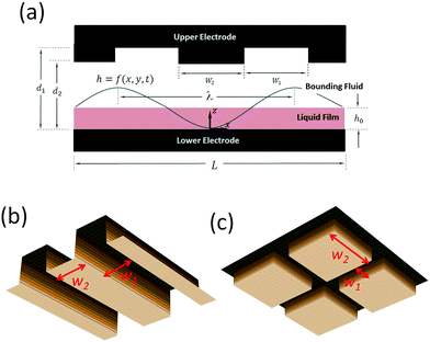
Electrohydrodynamic (EHD) destabilization of molten polymer or liquid films has received extensive attention over the past few decades as a unique and interesting approach for creating micron- and submicron-sized features for soft lithography1–16 and coatings.17,18 In this process, a thin liquid film is sandwiched between two electrodes and an electric field is applied to the film in the transverse direction (see Fig. 1). The disparity of electrical properties of the film and the bounding fluid (the material which fills the gap between the film and the upper electrode) results in a different electric field in each layer. As a consequence, a net electrostatic force acts at the interface due to the Maxwell stress.19 In the EHD patterning process, thicker regions of the film are subjected to a higher electrostatic force compared to thinner regions, thus the electrostatic force increases the instabilities. In contrast, capillary and viscous forces tend to dampen the instabilities. When the electrostatic force overcomes these damping forces, instabilities grow and pillars (raised columnar structures) form at the interface.1Initial linear stages in the growth of instabilities were investigated through linear stability (LS) analysis.1 The maximum wavelength for the growth of instabilities, (λ) which characterizes the center-to-center distance of pillars in a hexagonal pattern, is predicted by LS analysis.1–3 The LS analysis shows that the lateral size of pillars decreases by increasing the applied voltage (V), mean initial film thickness (h0), electric permittivity of the film (ε) and its conductivity (σ). Typically in the EHD patterning process, the thin liquid film is considered as either a perfect dielectric (PD) or a leaky dielectric (LD).1,6,11,20,21 Smaller length scales can be generated by introducing the temperature gradient for combined thermal and electric field induced instability for PD and LD thin films.22
In the PD film there is no free charge and the film is polarized under an applied electric field. In contrast, for the LD film the infinitesimal amount of charge present moves and accumulates at the interface. Both LS and non-linear analysis of EHD patterning demonstrate that the presence of free charges, albeit infinitesimal, reduces the characteristic wavelength λ.4,5,11,20,21 This is attributed to a high electrostatic force arising from the addition of an extra term to the Maxwell stress.16,23
Experiments showed that applying sufficiently a strong DC electric field to the thin liquid film or a pendant drop can destabilize the air–liquid interface leading to the formation of a conical shape, referred to as a DC Taylor cone.24–27 Subsequently, a drop is emitted from the cone's tip due to jet breaking. Such a EHD cone-jetting phenomenon, known as electrospraying, has been used extensively as a well-known technique of electrospray mass spectrometry.28,29
In the context of EHD patterning, the formation of the DC Taylor cone has just been reported (to the best of authors' knowledge) for the fabrication of the bifocal microlens using EHD reflowing of pre-patterned polymer films,30 where the steady state pattern formation is achieved using critical electric field intensity. The Taylor cone shape is observed when the electric field intensity slightly exceeds the critical value of 10 MV m−1 resulting in switching from ordinary single-focus microlenses to the bifocal ones. It should be noted that in the EHD patterning a finite mass is exposed to the electric field, in contrast with electrospraying, and the creeping flow (high viscosity and low velocity) hinders tip streaming and drop emissions.
The electric breakdown of a polymer film and the bounding fluid at a high electric field strength is reported as a limiting factor in EHD patterning especially when the fabrication of nano-sized features is needed.31 A significant discrepancy between theoretical predictions and experimental results (for both PDs and LDs) can also be attributed to this breakdown.31–33 Employing ionic conductive polymers or simply ionic liquid (IL) films as a bounding fluid enhances the electrostatic pressure acting at the interface while preventing electric breakdown.31 It is shown that in the polymer–ionic liquid bilayer system, the maximum wavelength (λ) can be decreased to a submicron level with an increase in the applied voltage and/or a decrease of polymer film thickness. However, it must be noted that thinner films have a higher tendency of dielectric breakdown mainly when the film thickness is less than 50 nm.31
Ionic conductive materials can be polymerized ionic liquids, ionic salt like materials (high temperature or low temperature), and aqueous or non-aqueous electrolytes.23,31,34–37 To mathematically model the ion distribution within the IL film the Poisson–Nernst–Plank (PNP) model has been used.23,31,35 When the process time is much shorter than the free charge/ion relaxation time the PNP equation can be simplified to the Poisson–Boltzmann equation which relates the electric potential to the charge distribution across the film.23,31
Free ions present in ILs move easily and form a diffuse layer called a double layer (DL) adjacent to the charged surfaces. In the PD and LD models, it is assumed that the thickness of the DL is infinitesimally large and small, respectively. Initially, to bridge the gap between these two limiting cases, an electrokinetic model was developed for drop deformation in an electric field.38,39 Recently an electrokinetic model has also been developed to study EHD patterning and LS analysis is used to investigate the dynamics of polymer films.23 These electrokinetic models apply the linearized Debye–Huckel approximation40 to study the stability of IL films. In our previous work, a more general model has been developed based on the nonlinear Poisson–Boltzmann equation to investigate the dynamics and stability of IL-PD bilayers.12,15 The EHD patterning process has also been conducted for ion conductive films which resulted in the creation of nano-sized pillars on the film even for high filling ratios (initial film thickness to electrode distance ratio).16 However, the formed pillars were polydispersed in the domain and less likely to have the array of pillars uniformly distributed over the domain.
In order to create well-ordered structures via electrically induced patterning, it is common to use a patterned mask which causes replication of mask on the polymer film.2,3,7,13,14 In this study, a patterned upper electrode is used to electrostatically control the spatial ordering of pillars as well as their sizes in an IL film. First, spatiotemporal evolution of thin PD and IL films in the absence of electrostatic heterogeneity (by using flat electrode) is presented as a baseline. Then the influence of electrostatic heterogeneity on the electric-field-induced destabilization of thin IL and PD films is presented. The effect of protrusion shape (strip and square block protrusions) and their size (see Fig. 1(b and c)) on the dynamics, morphological evolution and the pattern formation process of IL films is investigated and the results are compared with the PD base cases.
2 Mathematical model
A schematic of a thin liquid film resting on a lower electrode and confined with a patterned upper electrode (i.e. mask) is shown in Fig. 1(a). The gap between the film and the mask can be filled with air or a polymer. It is assumed that the material properties of the layers, such as interfacial tension, viscosity and dielectric permittivity, are constant. Gravity effects are neglected and it is assumed that the liquid film is incompressible Newtonian fluid. Constants and parameters used in this study are presented in Table 1.| Parameter | Value |
|---|---|
| interfacial tension (γ) | 0.045 N m−1 |
| Viscosity of liquid film (μ) | 1 Pa s |
| Effective Hamaker constant (A) | −1.5 × 10⁻²¹ J |
| Permittivity of vacuum (ε0) | 8.85 × 10⁻¹² C V−1 m−1 |
| Electric permittivity of thin film (ε1) | 2.5 (−) |
| Electric permittivity of bounding fluid (ε2) | 1 (−) |
| Mean initial film thickness (h0) | 20–70 nm |
| Electrodes distance (d1 and d2) | 80–300 nm |
| Protrusions width (W1) | 0.64–2.56 μm |
| Groove width (W2) | 0.64–2.56 μm |
| Equilibrium distance (l0) | 1 nm |
| Applied voltage (V) | 20 V |
| Molarity (M) | 0.0001 mol L−1 |
| Boltzmann constant (kB) | 1.3806488 × 10⁻²³ m2 kg s−2 K−1 |
| Avogadro's number (NA) | 6.022 × 10²³ mol−1 |
Continuity and Navier–Stokes (NS) equations are used to describe the thin film dynamics:
∇·![[u with combining right harpoon above (vector)]](https://www.rsc.org/images/entities/i_char_0075_20d1.gif) i = 0 i = 0 | (1) |
 | (2) |
![[f with combining right harpoon above (vector)]](https://www.rsc.org/images/entities/i_char_0066_20d1.gif) e = −∇ϕ stands for the external body force which consists of the intermolecular and electrostatic forces with the term ϕ being the conjoining/disjoining pressure. The subscript i = 1, 2 represents the ith fluid phase. Boundary conditions are:
e = −∇ϕ stands for the external body force which consists of the intermolecular and electrostatic forces with the term ϕ being the conjoining/disjoining pressure. The subscript i = 1, 2 represents the ith fluid phase. Boundary conditions are:![[u with combining right harpoon above (vector)]](https://www.rsc.org/images/entities/i_char_0075_20d1.gif) i = 0 at z = 0 & z = d1 and d2 i = 0 at z = 0 & z = d1 and d2 | (3) |
![[u with combining right harpoon above (vector)]](https://www.rsc.org/images/entities/i_char_0075_20d1.gif) relative = 0 at z = h(x,y,t) relative = 0 at z = h(x,y,t) | (4) |
 | (5) |
In this study, air is considered as the bounding fluid. Air is considered dynamically inert since it has much lower viscosity than the polymer film. Moreover, the Reynolds number in the EHD patterning process is much less than unity due to the small length scale of the system. The film motion can thus be described by Stokes flow. Combining these assumptions and applying lubrication theory to the thin film dynamics42 result in the following nonlinear thin film equation:
| 3μht + [h3(γ[hxx +hyy] − ϕ)x]x + [h3(γ[hxx + hyy] − ϕ)y]y = 0 | (6) |
The term, ϕvdW = A/6πh3, is the van der Waals pressure and A is the effective Hamaker constant defined as  in which 1, 2 and 3 denote the substrate, the liquid film and the bounding fluid. The term ϕBr = 8BU/(d − h)9 is the Born repulsion acting at the interface to avoid the contact line singularities when the interface touches the upper electrode. Coefficient BU is calculated by setting the conjoining pressure (ϕ) equal to zero at an equilibrium distance (l0). The electrostatic component of the conjoining pressure (ϕE) is found based on the Maxwell stress acting at the fluid interface19 as:
 | (7) |
 | (8) |
 ,
,  ,
,  and
and  results in:45
 | (9) |
The process time is τp = μh0/ε0ε1V02, and the charge relaxation time is τc = ε0ε1/σ. In this study, τp and τc are in the order of seconds and micro-seconds, respectively. This diminishes the effect of the free ion (charges) dynamics during the pattern formation process and the ion conservation equation (eqn (8)) is simplified to the Poisson–Boltzmann equation:40
 | (10) |
 is the Boltzmann distribution of free charges or ions and is zero for air. Vref is the reference potential which is found based on the electroneutrality conditions within the IL film,40
 . The term kBT represents the thermal motion where kB is the Boltzmann constant and T (K) is the temperature. The bulk ion number concentration n∞ = 1000NAM depends on the electrolyte molarity, M (mol L−1).
For the IL layer, the Poisson–Boltzmann equation and for air as PD bounding fluid the Laplace equation in the long-wave limit form are given as
 | (11) |
| V1 = V at z = 0; V2 = 0 at z = d |
| V1 = V2 and ε1(∂V1/∂z) = ε2(∂V2/∂z) at z = h(x,y,t) | (12) |
The Debye–Huckel approximation was used to simplify and analytically solve the electrostatic governing equations16,23 (eqn (11)). This results in a relation for the electrostatic pressure acting at the interface of the IL film bounded with air as
 | (13) |
 and Vs is calculated as:
 | (14) |
 | (15) |
In the presented mathematical model, the following points are worth mentioning: (a) all simulations are terminated at 1 nm (minimum equilibrium distance), which is considered as the limit of the continuum assumption, (b) the analogy of symmetric mono-valent electrolytes is used to analytically relate the electrostatic force and DL thickness in ionic liquids, (c) the height between the two electrodes, and the finite volume of the confined liquid film result in divergence of the hydrodynamic retardation as the electric field intensity diverges which avoids Taylor-cone formation and tip streaming.
2.1 Scaling
The thin film equation (eqn (6)) is nondimensionalized using scaling parameters obtained from LS analysis15,16 as:| X = x/Ls, Y = y/Ls, T = t/Ts and Φ = ϕ/Φs |
where
 | (16a) |
| Ts = 3μγε22h03/[0.5ε0ε1(ε1 − ε2)V2] | (16b) |
| Φs = 0.5ε0ε1(ε1 − ε2)V2/(ε22h02) | (16c) |
2.2 Numerical method
To find the spatiotemopral evolution of the thin IL film, the 2D nonlinear thin film equation is solved numerically. Derivatives in spatial coordinates are discretized using finite difference and the resulting set of differential algebraic equations (DAE) are solved in time using an adaptive time step ODE solver. A square domain with a length of 4λm under periodic boundary conditions is used. Term λm is the characteristic wavelength based on the lower electrode distance. Uniform Cartesian grids with four different grid sizes (nx × ny) of 91 × 91, 121 × 121, 151 × 151 and 171 × 171 are examined to find the optimum grid size and the results are shown in Fig. 2. The grid size of 121 × 121 grid points is found to be an acceptable compromise between the accurate interface height growth and the computational cost. Volume conservative random perturbations are used to initiate the film height of the simulations.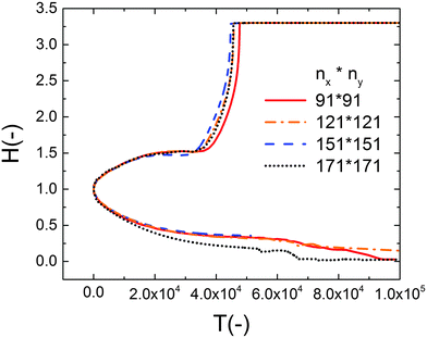 | ||
| Fig. 2 Effect of grid size on the nondimensional maximum and minimum interface height variations versus nondimensional time. The PD film with a mean initial thickness of h0 = 30 nm, V = 20 V. | ||
3 Results and discussion
3.1 Morphologies in the homogeneous electric field
In this section, an overview of the EHD patterning process under a homogeneous electric field is provided. The effects of ionic conductivity and the film initial filling ratio (mean initial film thickness to electrodes distance ratio) on the shape and size of structures are shown. Snapshots in time of the 3-D patterns for thin PD and IL liquid films (d1 = d2 = 100 nm) are presented in Fig. 3. Results show that the addition of ionic conductivity to the film results in an increase in the number of pillars forming at the interface and consequently more compact structures (pillars with smaller size) are created. The number of pillars formed in the IL films is also increased at higher filling ratios. The PD film shows a similar trend below the critical filling ratio of h0/d = 0.5. More details regarding the process of pattern formation and the structure size under a homogeneous electric field in ionic conductive films are presented elsewhere.16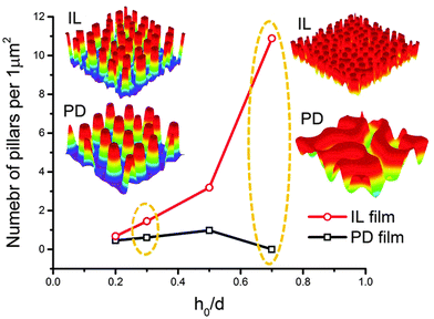 | ||
| Fig. 3 Total number of pillars versus initial filling ratio of the film. 3-D snapshots of the patterns formed in PD and IL films with h0 = 30 and 70 nm. d1 = d2 = 100 nm, V = 20 V. | ||
Base case studies demonstrate that the addition of ionic conductivity to the polymer film leads to more compact but less ordered pillars. Coarsening of the structure occurs randomly over the domain16 similar to the PD46,47 films resulting in non-uniform patterns. In PD films, the hexagonally packed pillars typically span about 10 to 15 pillars or they are randomly distributed over the domain.46 To overcome this limitation, a patterned mask is used to electrostatically control the structure size and fluid patterns. The use of a patterned mask, which results in the replication of the mask on the polymer film, has already been investigated for the PD and LD films.2,3,6,7,9,11,13,14,48 Fabricating controllable submicron sized structures using the EHD patterning process is the main objective of this study and the influence of electrostatic heterogeneity on the EHD pattern formation of thin IL films is investigated.
3.2 Conjoining/disjoining pressure
The final shape and size of features in the EHD patterning process are a result of a balance between the electrostatic (as the main driving force), intermolecular, viscous and interfacial force.49 The distribution of conjoining/disjoining pressure components acting at the film interface under a heterogeneous electric field is compared in Fig. 4. The 2-D cross-section height profile of the upper electrode and the patterned film is shown in Fig. 4(a and b), respectively. The Laplace pressure (Fig. 4(c)), the van der Waals pressure (Fig. 4(d)) and electrostatic pressure for the PD (Fig. 4(e)) and IL (Fig. 4(f)) films are all scaled with the electrostatic pressure acting on the PD film at the initial stage (flat interface) when exposed to the homogeneous electric field (d1 = d2 = 100 nm and h0 = 30 nm).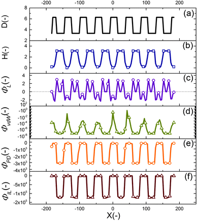 | ||
| Fig. 4 2-D non-dimensional profile of (a) upper electrode, (b) patterned film interface, (c) Laplace pressure, (d) van der Waals pressure, electrostatic pressure acting on (e) PD and (f) IL films. | ||
Negative (positive) pressure values in Fig. 4 represent the upward (downward) direction in which the interface is pushed toward the upper (lower) electrode. The electrostatic pressure has a negative value over the domain irrespective to the interface pattern but its magnitude changes significantly with the interface height (Fig. 4(e and f)). The film is exposed to a higher electrostatic force under protrusions (decreased electrode distance) caused by a lower electric potential drop in the bounding layer. Thinner film regions also experience lower electrostatic pressure compared to the thicker regions (located under protrusions), which results in fluid flowing from thinner regions to thicker regions. This confirms the destabilizing role of the electrostatic pressure in the EHD patterning process.
The curvature of the interface determines the Laplace pressure with a convex shape of the interface (in the valleys) resulting in negative values for pressure and vice versa (Fig. 4(c)). Film regions with a higher (lower) interface height experience a pressure toward the lower (upper) electrode. As a consequence, the Laplace pressure tends to flatten the interface, thereby stabilizing the film in contrast to the destabilizing effect of electrostatic pressure.
Short ranged van der Waals forces are considered in the simulation of the EHD pattering process when the film thickness is less than 100 nm. The van der Waals forces depend on the properties and surface energy of materials used for electrodes, films and the bounding fluid. In the present work, the lower electrode surface (apolar substrate) has a higher energy compared to the liquid film leading to a spinodally stable film (negative values for the pressure, shown in Fig. 4(d)) for the initial stage of the EHD patterning process.
Using a patterned electrode applies a heterogeneous pressure at the film interface leading to replication of the upper electrode pattern onto the polymer film (Fig. 4(a and b)). The distribution of scaled electrostatic pressure (ΦES) acting on the IL film at the initial stage (i.e. flat interface) is compared with a PD film as shown in Fig. 4(e) and (f). A smaller electrode distance results in a higher electrostatic pressure in both ILs and PDs; however, the IL films experience higher electrostatic pressure compared to the PD films in the protrusion regions (38 times higher in the case considered here).
3.3 Morphologies in the heterogeneous electric field
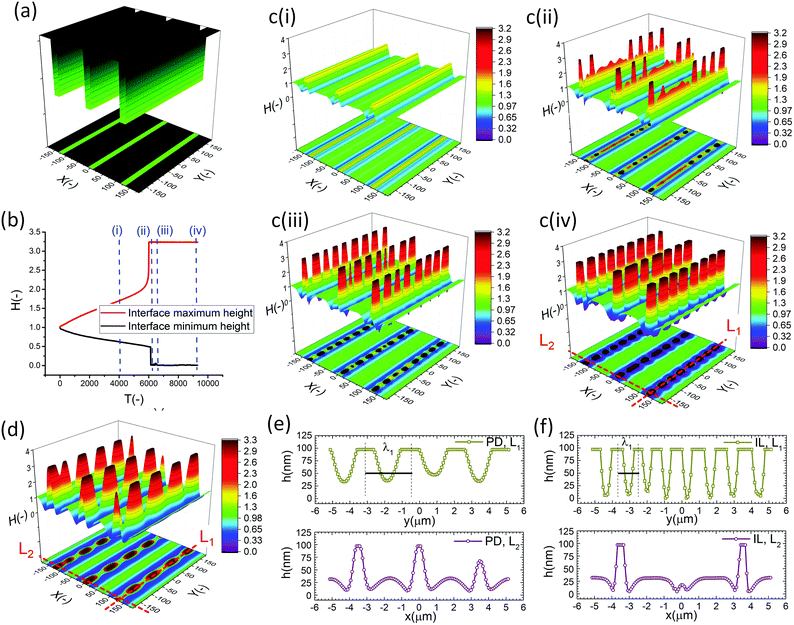
The effect of a heterogeneous electric field on the EHD patterning of PD and IL films using strip like and block protrusions is discussed. Effects of the size and shape of the patterns and the initial filling ratio on the EHD pattering process and the morphology of structures are investigated.For comparison, a 3-D snapshot of the PD film structure formed under similar conditions is shown in Fig. 5(d) which has much fewer pillars with oval cross-section formed under the protrusions. The cross-section height profiles (along the L1 and L2) provide more information regarding the size and shape of pillars in the PD and IL films (Fig. 5(e and f)). The center-to-center distance of adjacent pillars in the PD and IL films is around 2.6 and 1.2 μm respectively. A 53% reduction of the pillar width in the IL film, compared to the PD film, is achieved. The cross-section height profile along the X direction (L2) for the PD and IL films shows that the pillars are not necessarily aligned in the x direction. Hence the number of pillars and their shape may vary between the protrusion lines.
When a flat electrode is replaced with the patterned one, two characteristic spatial lengths are identified. The first is the spacing distance that pillars form within each protrusions (λ1) and the second characteristic length is the distance of pillars formed in two neighboring protrusions (λ2). The first one is controlled by the same parameters that affect the EHD patterning process of pattern-free electrodes such as the applied voltage, the film filling ratio and electric permittivity, etc. But the second one can also be controlled by adjusting the groove width.
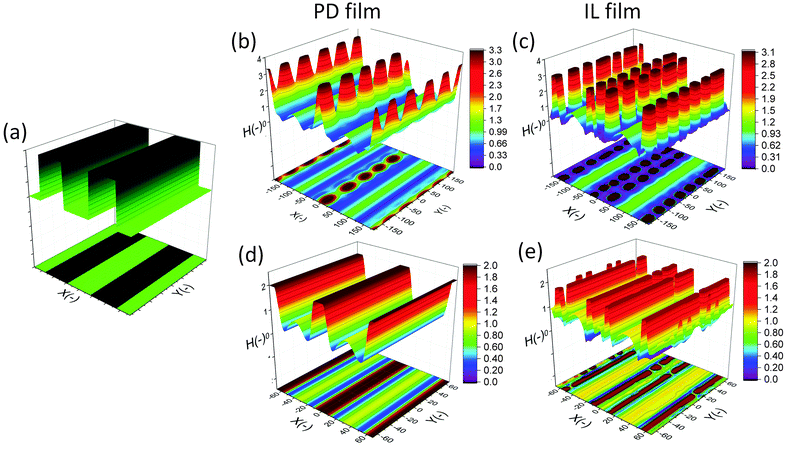
To investigate the effect of the patterned electrode on the IL films, the width of protrusions is increased from 0.64 to 2.46 μm. Structures formed at the quasi steady state stage (stage (iv) in Fig. 5(b)) of the EHD process are compared in Fig. 6. The height and applied voltage of protrusions are the same as in Fig. 5. Results for the PD and IL thin films with the mean initial thicknesses of 30 nm in Fig. 6(b and c) and 50 nm in Fig. 6(d and e) are presented. The 30 nm thick IL film forms two rows of pillars under the protrusion at the middle whereas in the PD film just one row of pillars is formed. In addition, the number of pillars formed in one row of the IL film is higher than in the PD film. For the 30 nm film thickness using a patterned electrode reduces the size of pillars in the IL films compared to a PD films. As previously mentioned, when a flat electrode is used, increasing the initial IL film thickness resulted in more compact structures with smaller sizes (see Fig. 3(b and c)). However, increasing the initial film thickness for the patterned electrode case results in the formation of roll-like structures.
The effect of reducing the groove width (w1) from 2.46 to 0.64 μm at a constant width of protrusions (2.46 μm) is investigated and the 3-D snapshots of the structures formed in the PD and IL films are shown in Fig. 7. The total number of pillars for the PD film is 12 whereas it exceeds 46 pillars for the IL film under the same conditions. By decreasing the width of grooves from 2.46 to 0.64 μm the undulating patterns are not formed under the grooves. Therefore the groove width should be smaller than the strip width to avoid secondary pattern formation in the low electric field (high gap) regions. Finally, by using an appropriately patterned electrode, smaller size features are generated and the structures are more compact and well ordered.
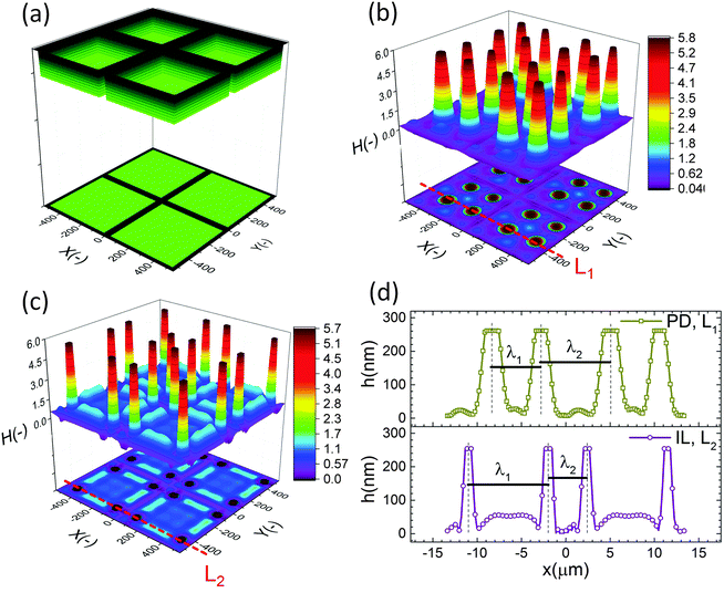
The cross-section height profile of the interface for the PD and IL films is compared in Fig. 8(d). The intra-array spacing of λ1 ∼ 5.9 μm and λ2 ∼ 8.3 μm in the PD film match the experimental observation48 of λ1 ∼ 6.2 μm and λ2 ∼ 8.8 μm with reasonable accuracy. This provides validation of the fidelity and accuracy of simulation results for the prediction of the pattern formed in the EHD process – at least for this case.
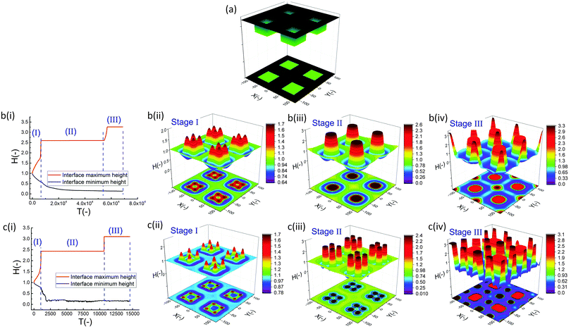
In the IL film, the center to center distance of pillars under the block protrusions is increased to λ1 ∼ 9 μm and the distance between the neighbor blocks is decreased to λ2 ∼ 4.5 μm. To create well ordered structures with a higher number of pillars, the electrode distances are reduced to d1 = 100 nm, d2 = 80 nm and an electrode mask with square protrusions (W1 = W2 = 0.84 μm) is used. A schematic of the upper electrode and spatiotemporal evolution of PD and IL films are shown in Fig. 9. Tracking the interface height over time (Fig. 9b(i)), it is found that the pattern formation includes three main stages. First, the interface is pushed toward the upper electrode in regions with a higher electrostatic force (under the protrusions) and castle shaped structures with four corner towers are formed. The cone shaped structures are formed close to the corners of squares as the gradient of electrostatic force is higher at these boundaries (Fig. 9b(ii) and c(ii)). Fluid depletion around boundaries (blue color ring in color print) is the evidence of fluid flow from thinner regions to the thicker ones. The cone shaped structure formed in the IL film is thinner compared to that formed in the PD film and at the corners, whereas in the PD film it is closer to the center. In the second stage, collision and coalescence of neighboring cones in the PD film occurs even before completion of the pillar formation. Hence, in the PD film, only one pillar is formed under the protrusions bridging the two electrodes (Fig. 9b(iii)) while in the IL film, four pillars with separate ring shaped fluid depletion are formed (Fig. 9c(iii)). In the third stage of pattern formation, secondary pillars are formed in the low electric field region (under the grooves) in both PD and IL films (Fig. 9b(iv) and c(iv)). In the IL film the four pillars formed under the protrusions are merged and form a pillar with a larger cross-section (similar to stage ii in the PD film), then the secondary pillars are created. The number of secondary pillars in the IL film is doubled compared to that in the PD film. Reducing the electrode distances d1 from 188 nm to 100 nm and d2 from 100 nm to 80 nm results in the formation of secondary pillars under the grooves. This can be used to create a multi-level structure.
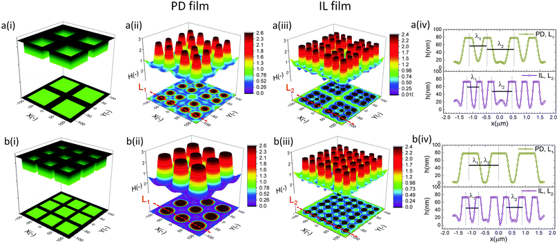
For further examining the effect of protrusion size, it is increased to W2 = 1.26 μm (=1.5 × λm) and the groove width is reduced to W1 = 0.42 μm (=0.5 × λm) as illustrated in Fig. 10a(i). As seen in Fig. 9b(iii) and c(iii), using protrusions with the same size as the characteristic wavelength for the growth of instabilities W2 = λm results in the formation of one (four) pillar(s) under the protrusions in the PD (IL) film. Increasing the protrusion size leads to the formation of four (nine) pillars in the PD (IL) film. The groove width is chosen narrow enough to avoid the formation of secondary pillars (Fig. 10a(ii and iii)). More detailed information regarding the size of pillars and their intra-spacing is shown in Fig. 10a(iv). The center to center distance of pillars formed under the protrusions (λ1) is reduced to ∼0.675 for the PD and 0.43 μm for the IL film. By reducing the groove width, the secondary pattern is no longer formed under the grooves for both PD and IL films. The distances between the neighboring pillars under the grooves (λ2) is around 1.0 and 0.78 μm in the PD and IL films, respectively.
The results show that for every n pillars that are formed with a PD film,  pillars would be created using an IL film under the same conditions. Although the number of pillars formed in the PD is less than the IL film, the size of pillars in the PD film are identical. In the case of the IL film, the pillars located at the center are smaller than those formed at the corners resulting in non-uniformity of pillar sizes. To have a maximum number of pillars with identical shape and size, a new pattern with nine uniform square block protrusions and the same patterning domain of 3.37 × 3.37 μm2 as Fig. 9(a) is used (see Fig. 10b(i)). From previous numerical results (Fig. 9b(iii) and c(iii)) it is expected to have one (four) pillar(s) under each protrusion in the PD (IL) film. Since only one pillar is formed under each protrusion in the PD film the center to center distance of pillars changes with the groove width (λ1 = λ2 ∼ 1.1 μm). In the IL film, the intra-array spacing of λ1 ∼ 0.47 μm and λ2 ∼ 0.6 μm is found to create similar sized structures over the patterning area and maximizes the number of pillars.
4 Conclusion
EHD patterning using a thin ionic conductive film and patterned electrodes is numerically examined to create compact (submicron level size) and well ordered structures. Dynamics and spatiotemporal evolution of thin PD and IL films, subjected to both homogeneous and heterogeneous electric fields, are investigated. Components of conjoining/disjoining pressure acting at the film interface during the EHD patterning process are compared. Higher electrostatic pressure acts at the interface of the IL films compared to the PD films. However, for both cases the electrostatic pressure distribution pattern over the domain matches the upper electrode pattern. Based on the 2D nonlinear thin film equation, the evolution of a three-dimensional structure is numerically simulated to find the dynamics and the process of pattern formation in the IL films and the results are compared with the PD baseline cases. For the PD base case results, structures formed at the quasi steady stage are in good agreement with the experiments48 in the literature and found to be within 5%.The effects of protrusion and groove size (width and depth) in strip like and square block patterns and the film initial filling ratio on the size, shape and order of fluid patterns are investigated. When the flat electrode is replaced with the patterned electrode, two characteristic spatial lengths are identified which are controlled by the width of the strip/square block (W2), groove width (W1) and groove depth (d1 − d2). Results show that depending on the groove width and depth the EHD patterning process has either two or three main stages. In the two-stage process, patterns only form under the protrusions whereas in the three-stage one, patterns (either undulating or secondary pillars) also form under the grooves. The two-stage process can be used for the pattern replication of mask onto the film and the three-stage one is utilized when the multilevel structure formation is desired. Furthermore, more pillars are found to be created using the IL film rather than the PD film. By using electrodes with square protrusions  pillars are formed in the IL film for every n pillars generated in the PD film. In the PD film, electrode square block mask protrusions with a width of W2 = 1.5 × λm and a groove width of W1 = 0.5 × λm and in the IL film square block protrusions with a width of W2 = λm and a groove width of W1 = 0.25 × λm result in compact and well ordered fluid pillars.
The key insight our electrostatic model provides is that, the leaky dielectric model may not account for phenomena important for EHD patterning, namely the presence of finite ions in the conducting layers. The Debye length is defined using ionic strengths, which provides a realistic range of free charge concentrations in the conducting fluid layer compared to the previous work in the literature.23 We expect that the results presented here will be useful for the creation of compact submicron sized features for optoelectronic-related applications.
References
- E. Schaffer, T. Thurn-Albrecht, T. P. Russell and U. Steiner, Nature, 2000, 403, 874–877 CrossRef CAS PubMed
.
- R. Verma, A. Sharma, K. Kargupta and J. Bhaumik, Langmuir, 2005, 21, 3710–3721 CrossRef CAS PubMed
.
- N. Wu and W. B. Russel, Nano Today, 2009, 4, 180–192 CrossRef CAS
.
- S. A. Roberts and S. Kumar, J. Fluid Mech., 2009, 631, 255–279 CrossRef
.
- S. A. Roberts and S. Kumar, Phys. Fluids, 2010, 22, 122102 CrossRef
.
- P. Goldberg-Oppenheimer and U. Steiner, Small, 2010, 6, 1248–1254 CrossRef CAS PubMed
.
- A. Atta, D. G. Crawford, C. R. Koch and S. Bhattacharjee, Langmuir, 2011, 27, 12472–12485 CrossRef CAS PubMed
.
- X. Xi, D. Zhao, F. Tong and T. Cao, Soft Matter, 2012, 8, 298–302 RSC
.
- L. Espin, A. Corbett and S. Kumar, J. Non-Newtonian Fluid Mech., 2013, 196, 102–111 CrossRef CAS
.
- Q. Yang, B. Q. Li and Y. Ding, Soft Matter, 2013, 9, 3412–3423 RSC
.
- K. Mondal, P. Kumar and D. Bandyopadhyay, J. Chem. Phys., 2013, 138, 024705 CrossRef PubMed
.
- H. Nazaripoor, C. R. Koch and S. Bhattacharjee, Proceedings of ASME. 46545, 2014, pp. 62-69.
- H. Tian, C. Wang, J. Shao, Y. Ding and X. Li, Langmuir, 2014, 30, 12654–12663 CrossRef CAS PubMed
.
- H. Li, W. Yu, Y. Wang, H. Bu, Z. Liu, E. Abraham and M. P. Y. Desmulliez, RSC Adv., 2014, 4, 13774–13781 RSC
.
- H. Nazaripoor, C. R. Koch and S. Bhattacharjee, Langmuir, 2014, 30, 14734–14744 CrossRef CAS PubMed
.
- H. Nazaripoor, C. R. Koch, M. Sadrzadeh and S. Bhattacharjee, Soft Matter, 2015, 11, 2193–2202 RSC
.
- A. Ramkrishnan and S. Kumar, Chem. Eng. Sci., 2013, 101, 785–799 CrossRef CAS
.
- A. Ramkrishnan and S. Kumar, Phys. Fluids, 2014, 26, 122110 CrossRef
.
-
L. D. Landau and E. M. Lifshitz, Electrodynamics of continuous media, Pergamon Press, 1960 Search PubMed
.
- L. F. Pease III and W. B. Russel, J. Chem. Phys., 2003, 118, 3790–3803 CrossRef
.
- L. F. Pease III and W. B. Russel, J. Non-Newtonian Fluid Mech., 2002, 102, 233–250 CrossRef
.
- A. Corbett and S. Kumar, J. Eng. Math., 2015, 94, 81–96 CrossRef CAS
.
- P. Gambhire and R. Thaokar, Phys. Rev. E: Stat., Nonlinear, Soft Matter Phys., 2014, 89, 032409 CrossRef PubMed
.
- G. I. Taylor, Proc. R. Soc. London, Ser. A, 1964, 280, 383–397 CrossRef
.
- J. Zeleny, Phys. Rev., 1917, 10, 1–6 CrossRef
.
- R. T. Collins, J. J. Jones, M. T. Harris and O. A. Basaran, Nat. Phys., 2008, 4, 149–154 CrossRef CAS
.
- G. Supeene, C. R. Koch and S. Bhattacharjee, J. Colloid Interface Sci., 2008, 318, 463–476 CrossRef CAS PubMed
.
- J. B. Fenn, M. Mann, C. K. Meng, S. F. Wong and C. M. Whitehouse, Science, 1989, 246, 64–71 CAS
.
- Y. Wang, M. K. Tan, D. B. Go and H-C. Chang, EPL, 2012, 99, 64003 CrossRef
.
- H. Hu, H. Tian, J. Shao, Y. Ding, C. Jiang and H. Liu, J. Micromech. Microeng., 2014, 24, 095027 CrossRef
.
- C. Y. Lau and W. B. Russel, Macromolecules, 2011, 44, 7746–7751 CrossRef CAS
.
- L. F. Pease and W. B. Russel, Langmuir, 2004, 20, 795–804 CrossRef CAS PubMed
.
- Q. Yang, B. Q. Li, Y. Ding and J. Shao, Ind. Eng. Chem. Res., 2014, 53, 12720–12728 CrossRef CAS
.
- H. Ohno, Macromol. Symp., 2007, 249–250, 551–556 CrossRef
.
- S. Majumdar, K. Kargupta and S. Ganguly, Polym. Eng. Sci., 2008, 48, 2229–2237 CAS
.
-
J. N. Israelachvili, Intermolecular and Surface Forces, Elsevier Inc., 3rd edn, 2011 Search PubMed
.
- M. A. Gebbie, M. Valtiner, X. Banquy, E. T. Fox, W. A. Henderson and J. N. Israelachvili, Proc. Natl. Acad. Sci. U. S. A., 2013, 110, 9674–9679 CrossRef CAS PubMed
.
- E. k. Zholkovskij, J. H. Masliyah and J. Czarnecki, J. Fluid Mech., 2002, 472, 1–27 CAS
.
- E. K. Zholkovskij, J. H. Masliyah, V. N. Shilov and S. Bhattacharjee, Adv. Colloid Interface Sci., 2007, 134–135, 279–321 CrossRef CAS PubMed
.
-
J. H. Masliyah and S. Bhattacharjee, Electrokinetic and Colloid Transport Phenomena, Wiley-Interscience, 2006 Search PubMed
.
- M. B. Williams and S. H. Davis, J. Colloid Interface Sci., 1982, 90, 220–228 CrossRef CAS
.
- A. Oron, S. H. Davis and S. G. Bankoff, Rev. Mod. Phys., 1997, 69, 931–980 CrossRef CAS
.
- A. Sharma and R. Khanna, Phys. Rev. Lett., 1998, 81(16), 3463–3466 CrossRef CAS
.
- A. Sharma and R. Khanna, J. Chem. Phys., 1999, 110, 4929–4936 CrossRef CAS
.
- D. A. Saville, Annu. Rev. Fluid Mech., 1997, 27–64 CrossRef
.
- H. Xiang, Y. Lin and T. P. Russell, Macromolecules, 2004, 37, 5358–5363 CrossRef CAS
.
- N. Wu, M. E. Kavousanakis and W. B. Russel, Phys. Rev. E: Stat., Nonlinear, Soft Matter Phys., 2010, 81, 26306–26319 CrossRef PubMed
.
- N. Wu, L. Pease and W. Russel, Adv. Funct. Mater., 2006, 16, 1992–1999 CrossRef CAS
.
- N. Wu and W. B. Russel, Ind. Eng. Chem. Res., 2006, 45, 5455–5465 CrossRef CAS
.
| This journal is © The Royal Society of Chemistry 2016 |



![[thin space (1/6-em)]](https://www.rsc.org/images/entities/char_2009.gif) 550, b(iii) 60
550, b(iii) 60