
Bright self-trapped exciton emission in alkali iodide nanocrystals via Sn(II)-doping†
Xuemeng
Wang
a,
Zan
Dou
a,
Cong
Tao
a,
Gaoyu
Chen
a,
Qi
Wei
b,
Haoyu
You
c,
Xiaowang
Liu
a,
Yatao
Zou
a,
Nannan
Han
a and
Weidong
Xu
 *ad
*ad
aFrontiers Science Center for Flexible Electronics, Xi’an Institute of Flexible Electronics (IFE), Northwestern Polytechnical University, 127 West Youyi Road, Xi’an 710072, China. E-mail: ifewdxu@nwpu.edu.cn
bDepartment of Applied Physics, The Hong Kong Polytechnic University, Hung Hom, Kowloon, Hong Kong
cShaanxi Provincial Key Laboratory of Papermaking Technology and Specialty Paper Development, College of Bioresource Chemical and Materials Engineering, Shaanxi University of Science & Technology, Xi’an 710021, P. R. China
dHenan Institute of Flexible Electronics (HIFE) and School of Flexible Electronics (SoFE), Henan University, 379 Mingli Road, Zhengzhou 450046, China
First published on 4th June 2024
Abstract
Lead-free alkali halides have gained increasing attention owing to their desired optoelectronic properties across a variety of light-emitting applications. However, state-of-the-art alkali halide emitters commonly are bulky crystals functionalized with highly toxic elemental doping, hindering their integration into emerging flexible, wearable and large-area optoelectronic devices. Herein, we have developed environmental friendly and solution-processable alkali halide nanocrystals that exhibit intense self-trapped emission facilitated by Sn2+ ionic doping. We find that the presence of Sn2+-interstitial leads to the tilting of cubic structures of RbI and thus triggers the self-trapped emission. The resultant tin(II)-doped RbI and RbxCs1−xI nanocrystals display an impressive maximum photoluminescence quantum yield of 91.9% and exhibit remarkable stability under ambient conditions. These findings pave the way for a new class of bright, solution-processable alkali halides, with diverse applications such as energy down conversion and flexible scintillation technologies.
 Weidong Xu | Weidong Xu has been a professor in the Institute of Flexible Electronics at Northwestern Polytechnical University since 2022. He received his PhD degree in Materials Science from Nanjing University of Posts and Telecommunications, China in 2016. Later, he moved to Linköping University, Sweden as a postdoc researcher and conducted principal research engineering (2017–2022). His group currently focuses on research on halide perovskites and lead-free metal halides for optoelectronics devices. |
1. Introduction
With the rising of metal halide perovskites in photovoltaics1 and light-emitting diodes (LEDs),2,3 lead-free metal halides have gained considerable attention due to their low toxicity and versatility in crystal structures, along with their varied optoelectronic properties. This study was focused on developing novel lead-free metal halides including lead-free perovskite ABX3, (e.g. CsSnX3 (X = Cl, Br, I)), A3B2X6 (e.g. Cs3Bi2I9), and double perovskites (e.g. Cs2AgInCl6).4–6 These compounds show promise in a range of applications beyond solar cells and LEDs,7 such as in X-ray8–11 and gamma-ray imaging, biological sensing,12 and as photodetectors.13Among lead-free metal halides, alkali halides such as NaI, CsI and RbI are well-known emitters with proven effectiveness in radioluminescence.14 In general, these materials are able to deliver bright emission and excellent light yields of around 40![[thin space (1/6-em)]](https://www.rsc.org/images/entities/char_2009.gif) 000–50000 ph per MeV.15 However, it is notable that their outstanding photoluminescence or radioluminescence emissions at room temperature are triggered by doping with highly toxic elements such as CsI: Tl and NaI: Tl, which are two of the most widely used scintillators for radiation detection and imaging since 1948.16 In addition, these materials were synthesized as bulky single crystals with high cost, making them hardly compatible with flexible and wearable applications. Considering their excellent emission properties and radioluminescence performance, it is highly promising to develop cost-effective and environmental friendly alkali halide emitters that are compatible with flexible and printing manufacturing techniques.
000–50000 ph per MeV.15 However, it is notable that their outstanding photoluminescence or radioluminescence emissions at room temperature are triggered by doping with highly toxic elements such as CsI: Tl and NaI: Tl, which are two of the most widely used scintillators for radiation detection and imaging since 1948.16 In addition, these materials were synthesized as bulky single crystals with high cost, making them hardly compatible with flexible and wearable applications. Considering their excellent emission properties and radioluminescence performance, it is highly promising to develop cost-effective and environmental friendly alkali halide emitters that are compatible with flexible and printing manufacturing techniques.
In this work, we achieved bright self-trapped exciton (STE) emission in rubidium iodide (RbI) nanocrystals at room temperature through Sn2+-doping. Specifically, with a mere 1.8% Sn incorporation, the RbI nanocrystals demonstrated broad-band yellow emission with a high photoluminescence quantum yield (PLQY) of approximately 91.9%, among the best for metal halides with STE emission. Theoretical analysis indicates that Sn2+ cations act as interstitials, causing tilts in the RbI crystal structure that generate sub-bandgap states conducive to STE emission. Furthermore, we could modulate the emission from yellow to orange by alloying with Cs+. Remarkably, our Sn2+-doped nanocrystals remain stable under ambient conditions without the need for encapsulation, contrasting the sensitivity of Sn-based perovskites to oxygen and moisture.17–19 Overall, our work not only unveils the first instance of alkali halide nanocrystals with bright emission at room temperature but also unlocks the potential of alkali halide emitters for a wide range of light-emitting applications such energy down conversion, flexible radioluminescence, and solar concentrators.
2. Experimental section
2.1 Chemicals
High-purity tin(II) iodide (SnI2, 99.999%), rubidium acetate (Rb(OAc), 99.8%), and tri-n-octylphosphine (TOP, 90%) were sourced from Alfa. Cesium carbonate (Cs2CO3, 99%) and oleic acid (OA, 90%) were acquired from Sigma-Aldrich. Oleylammonium iodide (OAmI, 99.5%), 1-octadecene (ODE, 90%), oleylamine (OLA, 90%), and xylene (99.0%, SafeDry) were procured from Adamas and Aladdin. Dowtherm A (referred to as DA) and ethyl acetate (EtOAc, 99.8%) were supplied by Macklin and Innochem. TOP, OA, OLA, and DA were pre-treated at 120 °C under vacuum for two hours to remove any moisture. Other reagents were used as received without further purification.2.2 Preparation process
:Rb feed ratio, with OAmI providing an additional source of iodine.
:1 v/v), and precipitated by centrifugation at 14000 rpm for 5 minutes. The resulting precipitate was collected and redispersed in xylene to create a colloidal dispersion of the NCs.
2.3 Characterization
3. Results and discussion
The synthetic protocols are shown in Fig. 1a. In brief, the Sn2+-doped RbI NCs were achieved by employing a classic hot injection method in an N2-filled glove box, where rubidium oleate (Rb-OA) precursor was quickly injected into SnI2/tri-n-octylphosphine (TOP) precursors. For reference purposes, we also prepared RbI NCs without the incorporation of Sn2+ cations, and the TEM image is shown in Fig. S1 (ESI†). We first started with 1-octadecene (ODE) as the solvent but realized that this commonly used solvent for synthesizing colloidal nanocrystals is not a good choice for those NCs with Sn2+. Our observations indicated that at high temperatures (≥120 °C), the SnI2–TOP solution in ODE transitions from yellow to brown, which is a typical sign of polyiodide formation because of the redox reaction during the synthesis of Sn2+-based nanocrystals.27 It consequently leads to uneven size distribution of NCs and the formation of a large number of crystal defects (Fig. 1b, upper panel), which usually are detrimental to the emission characteristics. | ||
| Fig. 1 (a) Synthetic procedures of Sn2+-doped RbI NCs by a hot injection method in a glove box, highlighting the critical role of different solvents (ODE and DA) in determining the quality of NCs. (b) TEM images of the NCs prepared with ODE (up panel) and DA (bottom panel) as the solvent (scale bar, 50 nm). (c) TEM image of optimized Sn2+-doped RbI NCs showing size distribution. (d) Absorbance and PL spectra of Sn2+-doped RbI NCs. (e) The dependence of PLQYs on the Sn:Rb feed ratio. | ||
To mitigate the formation of polyiodides, we utilized an aromatic mixture, Dowtherm A (referred to as DA, composed of 26.5% diphenyl and 73.5% diphenyl oxide) instead of the conventionally used ODE as the solvent,27 which is well-known for the excellent chemical stability. In addition, the electron-donating property of diphenyl oxide could be helpful for impeding the oxidation of Sn2+. The resulting nanocrystals exhibited a typical cubic shape with uniform size distribution (Fig. 1b, down panel). Further calculation yielded an average size of approximately ∼10 nm, as presented in Fig. 1c. Notably, a high injection temperature is key to realizing monodispersed size distribution, and the optimized temperature is 120 °C (Fig. S2, ESI†). In Fig. 1d, UV-vis absorption and PL emission spectra of Sn2+-doped RbI NCs are displayed. The PL spectrum features a broad-band emission peaking at 568 nm with a large full-width at half-maximum (FWHM) of 105.7 nm. The PL excitation (PLE) spectrum is displayed in Fig. S3 (ESI†), from which a serious of excitonic features are observed. The Stokes shift is ∼204 nm, as determined by the PLE peak with the lowest energy and PL emission. We note that the use of different solvents has no effect on the absorption and emission peaks but changes the photoluminescence quantum yield (PLQY) significantly (Fig. S4, ESI†). Fig. 1e illustrates the dependence of PLQYs of NCs as a function of the Sn2+:Rb+ feed ratio during synthesis. The highest PLQY, 91.9%, was achieved with a 40% molar ratio of Sn2+ relative to Rb+. This result contrasts sharply with that of the Sn2+-doped RbI NCs synthesized by ODE (24.3%). Besides, the over-addition of Sn2+ gives rise to a decrease in PLQYs, possibly due to the severe lattice distortion triggered by impurity doping.28,29 Notably, akin to RbI single crystals that do not emit at room temperature,30 this non-emissive property is also observed in their corresponding nanocrystals, suggesting the critical role of Sn2+ addition on triggering the emission properties.
To understand the mechanisms behind the PL emission of RbI NCs triggered by Sn2+ addition various structural characterizations were performed. Fig. 2a displays the morphological image of high-resolution transmission electron microscopy (HRTEM), where the presence of clear lattice fringes in the Sn2+-doped RbI NCs underscores their high crystallinity. The interplanar distance is 3.75 Å, slightly larger than the (200) plane of the cubic phase of RbI is 3.66 Å (Fig. 2a). Such an observation suggests lattice expansion as a result of Sn2+ doping.31 We show energy-dispersive spectroscopy (EDS) elemental mapping in Fig. 2b, from which homogeneous distributions of Rb+ and I− ions across the crystal matrix are clearly visible. Notably, despite substantial incorporation of SnI2 during the synthesis process (Rb:Sn molar ratio of 1:1), our EDS quantification reveals that only a small fraction of Sn2+ cations were retained, accounting for 1.86% of the total atomic composition (Fig. S5, ESI†).
 | ||
| Fig. 2 (a) A HRTEM image of the Sn2+-doped RbI NCs. (b) Elemental mapping for Rb, I and Sn, along with the relevant HAADF morphological image. (c) XRD patterns for RbI NCs and those with Sn2+ doping. (d) A focused comparison of the (200) crystal plane as extracted from the XRD patterns in Fig. 2c. (e) XPS core-level spectra of Sn 3d. | ||
Having confirmed the presence of Sn2+ in RbI NCs, we next performed X-ray diffraction (XRD) for the NCs thin films, aiming to determine whether the Sn2+ is incorporated within the crystal lattice or adsorbed on the crystal surface. Fig. 2c shows a comparison of the XRD pattern between pure RbI NCs and that after Sn2+ addition. We also show the standard JCPDS #78-635 card for reference. For both kinds of nanocrystals, the diffraction peaks well agreed with those from the references, suggestive of little changes in the crystal structures despite Sn addition. We also note that the doped samples show higher diffraction intensity and thus indicate a better crystallinity.32 Importantly, the XRD patterns for Sn-doped samples slightly shifted to lower two theta with respect to the reference samples as shown in Fig. 2d, suggesting an expansion of the crystal lattice.33 These results are in line with the HRTEM results, collectively confirming that Sn2+ ions are involved in the crystal lattice.
One consensus is that the divalent Sn ions are readily oxidized to quadrivalent once exposed to air, it is important to probe the valence of Sn cations and their chemical environment in the NCs. We thus performed X-ray photoelectron spectroscopy (XPS) for the doped and undoped samples. We show the XPS survey spectra in Fig. S6a (ESI†), and the core-level spectra of Sn 3d, Rb 3d and I 3d in Fig. 2e and Fig. S7 (ESI†). From Fig. 2e we see no evidence of Sn4+ formation, which is strikingly different from that in Sn2+-based perovskites. We also observed a downward shift in the binding energies of Rb 3d3/2 and 3d5/2 peaks by approximately 0.54 eV, and I 3d3/2 and I 3d5/2 peaks by approximately 0.13 eV. Such shifts suggest changes in the chemical environment and the redistribution of their electron cloud of Rb+ and I− upon Sn2+ incorporation. Considering the variations in the binding energy of Rb 3d and I 3d, we speculate that the enhanced difficulties in the formation of Sn4+ could be assigned to the redistribution of electron density due to charge transfer that stabilized Sn2+.
Having confirmed the incorporation of Sn2+ in the crystal lattice of RbI, we next performed a series of optical measurements to understand the photophysical behaviors of doped NCs. We realize that the large Stokes shift as well as the broad and symmetrical PL band are possibly the signs of emission from self-trapped excitons (STEs).34,35 To further investigate whether the bright emission comes from STEs or defect-mediated emission,36,37 we measured PL decay kinetics by time-correlated single-photon counting (TCSPC) technology. We show the PL decay curve in Fig. 3a, from which a double-exponential decay characteristic with a rapid yet minor decay component (∼200 ns, 6.2%) can be observed. The fast component can be attributed to charge trapping. The average lifetime is as long as ∼1050 ns, making it more likely to be STE emission. In addition, excitonic emission, such as STE emission, typically depends linearly on the excitation fluence,38 but the defects-mediated emission displays sublinear behavior due to the limited number of trap states. We thus conducted the fluence-dependent PL measurements. We show the integrated PL intensity as a function of excitation fluence (from 0.016 to 11.742 mW cm−2) in Fig. 3b, which clearly suggests a linear dependence. All these results indicate that the bright emission of Sn2+-doped RbI stems from STEs.
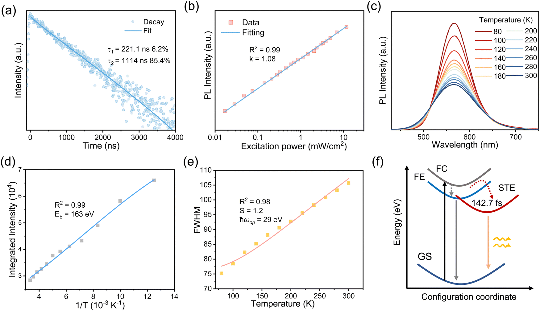 | ||
| Fig. 3 The optical characterization of Sn2+-doped RbI NCs. (a) TRPL decay curve. (b) Integrated PL emission intensity as a function of excitation power density. (c) Temperature-dependent PL spectra (80–300 K). (d) and (e) Integrated PL emission intensity (d) and FWHM (e) as a function of the temperature extracted from Fig. 3c. (f) The energy diagram depicting the STE processes. Here GS, FE, and FC refer to ground states and the states for free excitons and free carriers, respectively. | ||
In this regard, we proceeded to measure the temperature-dependent PL (80–300 K). As shown in Fig. 3c, the PL intensity increases with decreasing temperatures, owing much to the decreases in electron–phonon coupling or thermal-enhanced charge trapping.39Fig. 3d depicts the integrated PL intensity as a function of temperatures, where exciton binding energy was calculated by fitting the Arrhenius equation:40,41
 | (1) |
Furthermore, we investigated the PL line broadening as a function of temperature to understand the electron–phonon coupling, which is closely related to the full width at half maximum (FWHM) of the emission bands. The broadening was analyzed using the following relation:42
 | (2) |
To thoroughly understand the origin of STE emission, we conducted density functional theory (DFT) calculations to explore the potential sub-bandgap states arising from the addition of Sn2+ ions. We started from the model of pristine RbI cells (2 × 2 × 2) comprising 64 atoms. Accordingly, we introduced a Sn atom into the unit cell, placing it between the Rb and I atoms as an interstitial impurity. The resulting Sn–I interatomic distance was approximately 3.20 Å. The introduction of the interstitial Sn2+ leads to the expansion of the unit cells from 14.98 Å to 15.10 Å, as a result of its large ionic radius and the enhanced lattice distortion. The band structures, computed using the PBE exchange–correlation function, are depicted in Fig. S8 and S9 (ESI†). For the pristine RbI, a direct bandgap of 3.77 eV is observed (Fig. S9, ESI†). In comparison, the introduction of Sn interstitials gives rise to three discernible sub-bandgap states, two of which are deep-lying states and indicate possible effects on optical transitions (Fig. S9c, ESI†), in line with the appearance of PLE bands. The density of states (DOS) diagrams in Fig. 4b show that Sn contributes to all the generated sub-bandgap states, especially those near the conduction bands. Further analysis of orbital-projected DOS suggests the critical role of Sn 5p orbitals in creating sub-bandgap states. All in all, we deduce that the Sn atomic orbitals hybridize with the crystal states of the host lattice, leading to sub-bandgap states corresponding to STE emission.
 | ||
| Fig. 4 (a) Supercell of cubic RbI with an interstitial Sn atom. (b) Total and partial DOS Sn-doped RbI calculated by the PBE method. (c) Orbital-projected DOS for Sn2+-doped RbI calculated by the PBE method. The inset features an expanded view to highlight the sub-bandgap states. | ||
To assess the air stability of Sn2+-doped RbI NCs, we measured their PLQYs over time under ambient conditions, with a humidity of approximately 35–55%. Fig. 5a shows that the PLQY of the NC thin films retains over 80% of its initial value after 10 hours of air exposure. Moreover, even after three weeks in the air, the thin films were still emissive. These findings suggest that our Sn2+-doped RbI NCs are more resistant to oxygen and moisture than Sn-based perovskites, as detailed in Table S1 (ESI†). This much-enhanced stability may be attributed to the low Sn2+ content and/or the influence of the local electric structure, which could give rise to the different oxidation potential of Sn2+. Overall, combined with their good stability, the excellent optical properties of these materials, such as their bright emission with high quantum yields and large Stokes shifts, make them ideal for energy down-conversion applications, such as solar concentrators for silicon solar cells.44 Additionally, their potential for radiation detection and imaging is promising, considering the inclusion of heavy metal cations and the widespread use of CsI: Tl.14
 | ||
| Fig. 5 (a) PLQYs of Sn2+-doped RbI NCs over time under ambient conditions. (b) PL spectra of Sn2+-doped RbxCs1−xI NCs with different content of Cs+ during synthesis. | ||
We also synthesized Rb+/Cs+ alloyed NCs by doping with Sn2+, aiming to both demonstrate the versatility of our method and adjust the emission wavelengths. As shown in Fig. 5b, the PL spectra exhibited a red shift from 560 nm to 575 nm with the Cs+ ratio increasing from 0% to 40%, resulting in a color change from yellow to orange. Such a shift can be assigned to the larger ionic radius of Cs+ compared to that of Rb+, which leads to the lattice expansion once Cs+ is incorporated into the crystal structure. This speculation is supported by the XRD patterns shown in Fig. S10 (ESI†), which show a shift towards lower angles with higher Cs+ concentrations. However, further increasing the Cs+ content does not significantly affect the PL emission (Fig. S11, ESI†) or alter the XRD patterns. In addition, we found that it is very challenging to synthesize Sn2+-doped CsI nanocrystals. Since CsSnI3 conforms to Goldschmidt's rule for perovskite formation,4,45 we speculate that there are competitive reactions toward the formation of CsSnI3 and of Sn2+-doped CsI during synthesis. This could result in non-uniform nucleation and crystallization. Consistently, we observe notable variations in size and an irregular shape of RbxCs1−xI nanocrystals (Fig. S12, ESI†), as well as decreased PLQYs with enhancement of Cs+ content (Table S2, ESI†).
4. Conclusion
In summary, we have achieved strong and broadband emission in RbI nanocrystals via Sn2+ doping, delivering an impressive photoluminescence quantum yield of 91.9%. Such a bright yellow-light emission is attributed to the formation of self-trapped excitons, which arise from the incorporation of Sn2+ cations into RbI crystal lattices as interstitials and relevant generation of the sub-bandgap states. Furthermore, we have shown the capability to adjust the emission color by alloying with other alkali cations. Importantly, these Sn2+-doped lead-free metal halide nanocrystals demonstrate remarkable shelf stability in air, in stark contrast to the air-sensitivity of the Sn-based perovskites, thereby paving the way for their potential applications in various light-emitting technologies.Conflicts of interest
The authors declare no conflict of interest.Acknowledgements
This work was supported by the National Natural Science Foundation of China (Grants 52250060, 62274135, 62288102, 52302167), Key project of Ningbo Natural Science Foundation (Grants 20221JCGY01049), the China Postdoctoral Science Foundation (Grants GZB20230975).References
- P. V. Kamat, J. Bisquert and J. Buriak, ACS Energy Lett., 2017, 2, 904–905 CrossRef CAS
.
- W. Xu, Q. Hu, S. Bai, C. Bao, Y. Miao, Z. Yuan, T. Borzda, A. J. Barker, E. Tyukalova, Z. Hu, M. Kawecki, H. Wang, Z. Yan, X. Liu, X. Shi, K. Uvdal, M. Fahlman, W. Zhang, M. Duchamp, J.-M. Liu, A. Petrozza, J. Wang, L.-M. Liu, W. Huang and F. Gao, Nat. Photonics, 2019, 13, 418–424 CrossRef CAS
- M. Karlsson, Z. Yi, S. Reichert, X. Luo, W. Lin, Z. Zhang, C. Bao, R. Zhang, S. Bai, G. Zheng, P. Teng, L. Duan, Y. Lu, K. Zheng, T. Pullerits, C. Deibel, W. Xu, R. Friend and F. Gao, Nat. Commun., 2021, 12, 361–371 CrossRef CAS PubMed
- Q. Liu, J. Yin, B.-B. Zhang, J.-K. Chen, Y. Zhou, L.-M. Zhang, L.-M. Wang, Q. Zhao, J. Hou, J. Shu, B. Song, N. Shirahata, O. M. Bakr, O. F. Mohammed and H.-T. Sun, J. Am. Chem. Soc., 2021, 143, 5470–5480 CrossRef CAS PubMed
- Y. Zhang, Y. Liu, Z. Xu, H. Ye, Z. Yang, J. You, M. Liu, Y. He, M. G. Kanatzidis and S. Liu, Nat. Commun., 2020, 11, 2304–2315 CrossRef CAS PubMed
- Y. Liu, A. Nag, L. Manna and Z. Xia, Angew. Chem., Int. Ed., 2021, 60, 11592–11603 CrossRef CAS PubMed
- Y. Zou, P. Teng, W. Xu, G. Zheng, W. Lin, J. Yin, L. Kobera, S. Abbrent, X. Li, J. A. Steele, E. Solano, M. B. J. Roeffaers, J. Li, L. Cai, C. Kuang, I. G. Scheblykin, J. Brus, K. Zheng, Y. Yang, O. F. Mohammed, O. M. Bakr, T. Pullerits, S. Bai, B. Sun and F. Gao, Nat. Commun., 2021, 12, 4831–4841 CrossRef CAS PubMed
- J. H. Han, T. Samanta, Y. M. Park, H. J. Kim, N. S. Manikanta Viswanath, H. W. Kim, B. K. Cha, S. B. Cho and W. B. Im, ACS Energy Lett., 2023, 8, 545–552 CrossRef CAS
- W. Pan, H. Wu, J. Luo, Z. Deng, C. Ge, C. Chen, X. Jiang, W.-J. Yin, G. Niu, L. Zhu, L. Yin, Y. Zhou, Q. Xie, X. Ke, M. Sui and J. Tang, Nat. Photonics, 2017, 11, 726–732 CrossRef CAS
- X. Ou, X. Qin, B. Huang, J. Zan, Q. Wu, Z. Hong, L. Xie, H. Bian, Z. Yi, X. Chen, Y. Wu, X. Song, J. Li, Q. Chen, H. Yang and X. Liu, Nature, 2021, 590, 410–415 CrossRef CAS PubMed
- Y. Liu, Y. Zhang, X. Zhu, J. Feng, I. Spanopoulos, W. Ke, Y. He, X. Ren, Z. Yang, F. Xiao, K. Zhao, M. Kanatzidis and S. Liu, Adv. Mater., 2021, 33, 2006010 CrossRef CAS PubMed
- J. Casanova-Chafer, R. Garcia-Aboal, P. Atienzar and E. Llobet, ACS Sens., 2022, 7, 3753–3763 CrossRef CAS PubMed
- A. Waleed, M. M. Tavakoli, L. Gu, Z. Wang, D. Zhang, A. Manikandan, Q. Zhang, R. Zhang, Y.-L. Chueh and Z. Fan, Nano Lett., 2017, 17, 523–530 CrossRef CAS PubMed
- S. Tsuda and K. Saito, J. Environ. Radioact., 2017, 166, 419–426 CrossRef CAS PubMed
- T. Igashira, N. Kawano, G. Okada, N. Kawaguchi and T. Yanagida, Optik, 2018, 155, 36–42 CrossRef CAS
- R. Hawrami, E. Ariesanti, A. Farsoni, D. Szydel and H. Sabet, Crystals, 2022, 12, 1517–1525 CrossRef CAS
- C. Kang, H. Rao, Y. Fang, J. Zeng, Z. Pan and X. Zhong, Angew. Chem., Int. Ed., 2021, 60, 660–665 CrossRef CAS PubMed
- L. Dai, Z. Deng, F. Auras, H. Goodwin, Z. Zhang, J. C. Walmsley, P. D. Bristowe, F. Deschler and N. C. Greenham, Nat. Photonics, 2021, 15, 696–702 CrossRef CAS
- Z. Chen and T. P. Dhakal, Appl. Phys. Rev., 2023, 10, 011404 CAS
- G. Kresse, J. Non-Cryst. Solids, 1995, 192, 222–229 CrossRef
- G. Kresse and J. Hafner, Phys. Rev. B: Condens. Matter Mater. Phys., 1994, 49, 14251–14269 CrossRef CAS PubMed
- G. Kresse and J. Furthmüller, Comput. Mater. Sci., 1996, 6, 15–50 CrossRef CAS
- G. Kresse and J. Furthmüller, Phys. Rev. B: Condens. Matter Mater. Phys., 1996, 54, 11169–11186 CrossRef CAS PubMed
- G. Kresse and J. Hafner, J. Phys.: Condens. Matter., 1994, 6, 8245 CrossRef CAS
- G. Kresse and D. Joubert, Phys. Rev. B: Condens. Matter Mater. Phys., 1999, 59, 1758–1775 CrossRef CAS
- J. P. Perdew, K. Burke and M. Ernzerhof, Phys. Rev. Lett., 1996, 77, 3865–3868 CrossRef CAS PubMed
- D. N. Dirin, A. Vivani, M. Zacharias, T. V. Sekh, I. Cherniukh, S. Yakunin, F. Bertolotti, M. Aebli, R. D. Schaller, A. Wieczorek, S. Siol, C. Cancellieri, L. P. H. Jeurgens, N. Masciocchi, A. Guagliardi, L. Pedesseau, J. Even, M. V. Kovalenko and M. I. Bodnarchuk, Nano Lett., 2023, 23, 1914–1923 CrossRef CAS PubMed
- B.-Q. Zhao, Y. Li, X.-Y. Chen, Y. Han, S.-H. Wei, K. Wu and X. Zhang, Adv. Sci., 2023, 10, 2300386 CrossRef CAS PubMed
- X. Lü, C. Stoumpos, Q. Hu, X. Ma, D. Zhang, S. Guo, J. Hoffman, K. Bu, X. Guo, Y. Wang, C. Ji, H. Chen, H. Xu, Q. Jia, W. Yang, M. G. Kanatzidis and H.-K. Mao, Natl. Sci. Rev., 2021, 8, nwaa288 CrossRef PubMed
- T. Harami, S. Kakigi and A. Okuda, J. Phys. Soc. Jpn., 1987, 56, 4157–4161 CrossRef CAS
- Y. Wang, Y. Jiao, H. Yan, G. Yang, C. Tian, A. Wu, Y. Liu and H. Fu, Angew. Chem., Int. Ed., 2022, 61, e202116233 CrossRef CAS PubMed
- W. Xu, B. Chen, Z. Zhang, Y. Liu, Y. Xian, X. Wang, Z. Shi, H. Gu, C. Fei, N. Li, M. A. Uddin, H. Zhang, L. Dou, Y. Yan and J. Huang, Nat. Photonics, 2024, 18, 379–387 CrossRef CAS
- K. Li, Y. Shao, H. Yan, Z. Lu, K. J. Griffith, J. Yan, G. Wang, H. Fan, J. Lu, W. Huang, B. Bao, X. Liu, C. Hou, Q. Zhang, Y. Li, J. Yu and H. Wang, Nat. Commun., 2018, 9, 4798–4809 CrossRef PubMed
- F. Zhang, D. Yang, Z. Shi, C. Qin, M. Cui, Z. Ma, L. Wang, M. Wang, X. Ji, X. Chen, D. Wu, X. Li, L. Zhang and C. Shan, Nano Today, 2021, 38, 101153 CrossRef CAS
- J. Zhou, M. Li, L. Ning, R. Zhang, M. S. Molokeev, J. Zhao, S. Yang, K. Han and Z. Xia, J. Phys. Chem. Lett., 2019, 10, 1337–1341 CrossRef CAS PubMed
- S. Tongay, J. Suh, C. Ataca, W. Fan, A. Luce, J. S. Kang, J. Liu, C. Ko, R. Raghunathanan, J. Zhou, F. Ogletree, J. Li, J. C. Grossman and J. Wu, Sci. Rep., 2013, 3, 2657–2662 CrossRef PubMed
- Y. Zhu, J. Lim, Z. Zhang, Y. Wang, S. Sarkar, H. Ramsden, Y. Li, H. Yan, D. Phuyal, N. Gauriot, A. Rao, R. L. Z. Hoye, G. Eda and M. Chhowalla, ACS Nano, 2023, 17, 13545–13553 CrossRef CAS PubMed
- Y. He, S. Liu, Z. Yao, Q. Zhao, P. Chabera, K. Zheng, B. Yang, T. Pullerits and J. Chen, J. Phys. Chem. Lett., 2023, 14, 7665–7671 CrossRef CAS PubMed
- M. B. Bebek, C. M. Stanley, T. M. Gibbons and S. K. Estreicher, Sci. Rep., 2016, 6, 32150–32158 CrossRef CAS PubMed
- K. Wu, A. Bera, C. Ma, Y. Du, Y. Yang, L. Li and T. Wu, Phys. Chem. Chem. Phys., 2014, 16, 22476–22481 RSC
- Z. Chen, C. Yu, K. Shum, J. J. Wang, W. Pfenninger, N. Vockic, J. Midgley and J. T. Kenney, J. Lumin., 2012, 132, 345–349 CrossRef CAS
- W. Stadler, D. M. Hofmann, H. C. Alt, T. Muschik, B. K. Meyer, E. Weigel, G. Müller-Vogt, M. Salk, E. Rupp and K. W. Benz, Phys. Rev. B: Condens. Matter Mater. Phys., 1995, 51, 10619–10630 CrossRef CAS PubMed
- C. M. Iaru, A. Brodu, N. J. J. van Hoof, S. E. T. ter Huurne, J. Buhot, F. Montanarella, S. Buhbut, P. C. M. Christianen, D. Vanmaekelbergh, C. de Mello Donega, J. G. Rivas, P. M. Koenraad and A. Y. Silov, Nat. Commun., 2021, 12, 5844–5852 CrossRef CAS PubMed
- M. B. de la Mora, O. Amelines-Sarria, B. M. Monroy, C. D. Hernández-Pérez and J. E. Lugo, Sol. Energy Mater. Sol. Cells, 2017, 165, 59–71 CrossRef CAS
- A. Morteza Najarian, F. Dinic, H. Chen, R. Sabatini, C. Zheng, A. Lough, T. Maris, M. I. Saidaminov, F. P. García de Arquer, O. Voznyy, S. Hoogland and E. H. Sargent, Nature, 2023, 620, 328–335 CrossRef CAS PubMed
Footnote |
| † Electronic supplementary information (ESI) available. See DOI: https://doi.org/10.1039/d4tc01428f |
| This journal is © The Royal Society of Chemistry 2024 |