 Open Access Article
Enhanced photoelectrochemical hydrogen production via linked BiVO4 nanoparticles on anodic WO3 nanocoral structures†
Eunoak
Park
 ,
JeongEun
Yoo
* and
Kiyoung
Lee
 *
*
Department of Chemistry and Chemical Engineering, Inha University, 100 Inha-ro, Michuhol-gu, 22212 Incheon, South Korea. E-mail: kiyoung@inha.ac.kr; JeongEunYoo@inha.ac.kr
First published on 26th February 2024
Abstract
Morphological properties of photoanodes are crucial for improving their photoelectrochemical (PEC) performance. In this study, we fabricated bismuth vanadate (BiVO4) nanoparticles (NPs) with an optimal size of ∼10 nm, as well as nanowires composed of NPs on anodized tungsten trioxide (WO3) nanocoral structures. The linked BiVO4 NPs were decorated by spin-coating, with the amount of the BiVO4 precursor being controlled. Subsequently, the concentrations of Bi and V in the BiVO4 precursor were determined. An optimized concentration of 0.3 M Bi and V for the linked BiVO4 NPs/WO3 nanocoral heterostructure led to enhanced photocurrent density and hydrogen gas-production compared to those of the pristine WO3 nanocorals, yielding results that were 2.4 times higher. In particular, the incident photon-to-current conversion efficiency value at 410 nm improved by 8.3 times, as the linked BiVO4 NPs attained efficient absorbance of visible light and a sufficient electron transfer pathway.
1. Introduction
Numerous efforts to produce hydrogen energy have been made using renewable energy from solar fuels to address the global energy crisis.1–3 In particular, photoelectrochemical water splitting (PEC-WS) has emerged as a promising green engineering approach for generating hydrogen through direct utilization of sunlight.4,5 For PEC-WS, metal oxide semiconductors are mostly used as photoelectrodes because of their beneficial bandgap and band positions for photoreactions.6 However, metal oxide semiconductor photoanodes face several critical issues, such as reduced solar-to-hydrogen efficiency of PEC-WS, slow surface water oxidation, poor visible light absorption, and fast electron–hole recombination.7,8Bismuth vanadate (BiVO4), the most promising metal oxide photoanode material for PEC-WS, has been investigated owing to its intrinsic properties such as abundance, nontoxicity, and low cost.9–11 BiVO4 also satisfies the requirements for an efficient photoanode by providing a narrow bandgap of 2.4 eV with a relatively negative conduction band edge of ∼0 V vs. the reversible hydrogen electrode (RHE), and having a high optical absorption coefficient (∼104–105 cm−1 at hν = 2.5–3.5 eV).12–14 Despite these advantages, BiVO4 still suffers from fast recombination of photogenerated electrons and holes because of its low carrier mobility (∼4.4 × 10⁻² cm2 V−1 s−1) and short hole diffusion length (∼70 nm).15,16
To overcome these drawbacks and enhance the photo efficiency of PEC-WS, BiVO4 often adopts a type-II heterojunction configuration with two or more n-type semiconductors. At the heterojunction interface between two semiconductors, a wide bandgap material offers a more negative conduction band (CB) edge, allowing electrons to move from the narrow bandgap material to the wide bandgap material.17 In this context, tungsten trioxide (WO3) (∼2.8 eV) has been considered the most suitable matching material for forming a type II heterojunction with BiVO4. This is because WO3 has a superior electron mobility (∼12 cm2 V−1 s−1), relatively long hole diffusion length (∼150 nm), and lower CB edge of +0.41 V vs. RHE compared to BiVO4.18–20 To fabricate WO3 for the configuration of the BiVO4/WO3 heterostructure, several simple approaches have been reported such as a hydrothermal method,17,21 dip-coating,22 spin-coating,23 and anodization.24 Among the various methods, the anodization method is an advantageous because W metal as a substrate can provide direct back contact under the WO3 layer and can form various nanostructures with a high specific surface area by adjusting the anodization conditions (e.g., electrolyte, temperature, applied potential, etc.). There is only one reported research study that used anodic WO3 for fabricating a BiVO4/WO3 heterostructure. However, the BiVO4/WO3 heterostructure of anodized WO3 structures and spin-coated BiVO4 layers has not fulfilled the role of a photoanode for PEC-WS, because the thick BiVO4 layer (∼850 nm) interrupts the mobility of photogenerated electrons from BiVO4 to WO3.25 Thus, it is obvious that rapid electron movement is allowed only when BiVO4 is as thin as a nanolayer or a nanoparticle (NP).10 In particular, metal oxide NPs have attracted attention in photoelectrochemical reactions as they provide a large reaction area, leading to improved photoreaction efficiency.
In this study, we have investigated how to fabricate BiVO4 NPs on anodic WO3. In addition, we developed BiVO4 NPs linked as nanowires to a WO3 nanocoral structure. This is the first study on the heterojunction of BiVO4 NPs and anodic WO3 nanocorals. The WO3 nanocoral structures on W metal were fabricated by the anodization method, as previously reported.22 The linked BiVO4 NPs were formed on the WO3 nanocorals by the spin-coating method where, instead of deionized water, we employed an ethylene glycol-based solvent as a BiVO4 precursor for the spin-coating process, since the utilization of the ethylene glycol-based BiVO4 precursor allows BiVO4 nanoparticles to form with sizes below 100 nm as supporting particle agglomeration on WO3 layers during spin-coating. The use of ethylene glycol as the solvent for the BiVO4 precursor has not been previously reported. Furthermore, we focus on the amount of the BiVO4 precursor used during spin-coating to construct linked BiVO4 NPs on WO3 nanocorals and determine their morphologies, crystal structures, and PEC performances with different precursor amounts. We then optimized the concentration of vanadium (V) in the BiVO4 precursor and investigated the morphologies, compositional properties, and PEC performance of the heterostructure of the BiVO4 NPs/WO3 nanocorals.
2. Experimental
2.1 Materials
The following materials were used as received: ammonium fluoride (NH4F, ≥ 98%, Sigma Aldrich), sodium sulfate (Na2SO4, ≥99.9%, Sigma Aldrich), bismuth(III) nitrate pentahydrate (Bi(NO3)3·5H2O, ≥98%, Sigma Aldrich), nitric acid (HNO3, 60%, Samchun Chemicals), ethylene glycol (HOCH2CH2OH, 99.5%, Samchun Chemicals), and ammonium metavanadate (NH4VO3, 99%, Daejung Chemicals & Metals).2.2 Preparation of the BiVO4/WO3 photoanodes
Tungsten (W) metal (thickness: 0.1 mm, 99.95% purity, Alfa Aesar) was cut into 1.5 × 1.5 cm2 and mechanically ground using a 1200 grit soft sandpaper. Next, the W metal was cleaned successively with acetone, ethanol, and deionized (DI) water using an ultrasonicator, and then dried with nitrogen (N2) gas. W metal was anodized in a 1 M Na2SO4 solution containing 0.5 wt% NH4F at 15 °C. The thickness of WO3 nanocorals was increased with increase in anodization time from 1 h to 5 h, to approximately 460, 540, 610, 660 and 690 nm, respectively. Among them, WO3 anodized for 3 h was used as the substrate. During anodization, a constant voltage of 40 V was applied to W using a DC power source (ODA-EX300-4), and current density versus time curves were recorded using a Keithley 2000. After anodization, the anodic WO3 nanocorals were rinsed with DI water and dried with N2 gas. Heat-treatment was performed in a tubular furnace at 500 °C under an argon (Ar) atmosphere for 2 h to crystallize the anodized WO3 nanocoral film. Then, the BiVO4 NPs were decorated onto the WO3 nanocoral films by spin-coating. The BiVO4 precursor solution for spin-coating was prepared by dissolving 0.15 (0.3), 0.23 (0.44), 0.3 (0.59), and 0.6 M (1.18) NH4VO3 in a mixture of 10 mL HNO3 and 20 mL ethylene glycol. After complete dissolution, 0.3 M (2.25) Bi(NO3)3·5H2O was added and then the solution was stirred for 30 min. After dropping 5, 10, and 30 μL of the precursor onto the WO3 substrate, the samples were rested for 1 min so that the precursor penetrates to the bottom of the nanocoral structures. The spin-coating process was performed at 500 rpm for 60 s, 1000 rpm for 30 s, and 3000 rpm for 3 s for the precursor mixture solution and was repeated 3 times. Between each cycle, the BiVO4/WO3 samples were heat-treated in a box furnace at 100 °C for 5 min. After the spin-coating process, the samples were annealed at 550 °C under an air atmosphere using the box furnace for 1 h.2.3 Characterization
The morphologies of the WO3 and BiVO4/WO3 photoanodes were observed using a field-emission scanning electron microscope (FE-SEM, S-4300, Hitachi). To characterize the crystalline structures of the photoanodes, X-ray diffraction (XRD, X'Pert PRO MRD, Phillips) with a Cu-Kα radiation source and field emission transmission electron microscopy (FE-TEM, JEM-2100F, JEOL) were used. Raman scattering measurements (LabRAm HR Evolution, HORIBA) were obtained using 532 nm lasers. The analysis was conducted at the Inha University Core Facility Center for Sustainable Energy.2.4 Photoelectrochemical measurements
0.5 M Na2SO4 solution, silver/silver chloride (Ag/AgCl, 3 M KCl), a Pt mesh, and BiVO4/WO3 photoanodes were used as the electrolyte, and reference, counter, and working electrodes, respectively. Photocurrent density, electrochemical impedance spectroscopy (EIS), and hydrogen (H2) gas production were measured using a potentiostat (VSP, Bio-Logics) and a solar simulator (LCS-100, Oriel Instruments) with a 100 W xenon (Xe) arc lamp (100 mW cm−2). To record the photocurrent density, linear sweep voltammetry (LSV) was performed at a scan rate of 5 mV s−1. The obtained potential was converted into a RHE potential using the following equation:| ERHE = EAg/AgCl + (0.0591 × pH) + EAg/AgCl° |
| EAg/AgCl (3 M KCl) = 0.1976 V at 25 °C |
EIS was performed in the range of 30 kHz–10 MHz at 1.23 V vs. RHE. To evaluate PEC H2-gas production at 1.23 V vs. RHE, 200 μL gas was taken from the sealed quartz tube reactor every half hour and injected into a gas chromatograph with a TCD detector (GC/MSD 5975C, Agilent Technologies). The incident photon-to-current conversion efficiency (IPCE) was measured at 1.23 V vs. RHE using a monochromator (MonoRa200, DONGWOO OPTRON) and various bandpass filters with a Xe lamp (300 W, OMA). The IPCE was calculated using the following equation:
3. Results and discussion
3.1 Formation of linked BiVO4 NPs on WO3 nanocorals
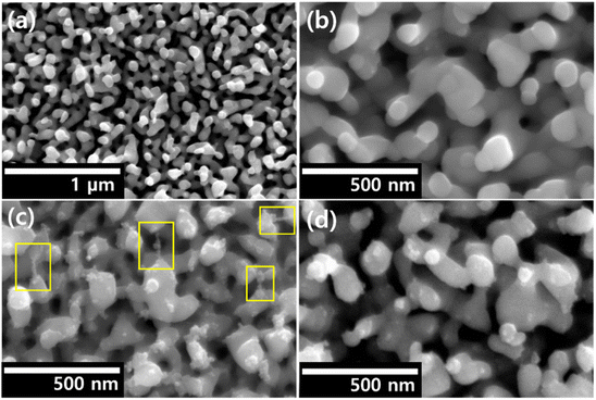
Fig. 1a shows the morphology of WO3 nanocoral anodized W metal described in our previous report.24 The WO3 nanocorals have thick branches and round edges with a high surface area, which can support the formation of NPs, and the length of the nanocoral structures is ∼550–600 nm (Fig. S1†). All the BiVO4/WO3 (BW) heterostructures formed by the anodization and spin-coating processes contained BiVO4 NPs on the WO3 nanocorals as presented in Fig. 1b–d. During the spin-coating process, the precursor amounts were controlled to be 5, 10, and 30 μL, and the heterostructural BiVO4 NPs/WO3 nanocorals fabricated with these precursor amounts were labelled as 5-BW, 10-BW, and 30-BW, respectively. Following heat treatment in air, a 5–10 nm size of the well-spread BiVO4 NPs was observed on the WO3 nanocorals. The formation of BiVO4 NPs on the nanocorals was related to the hydrophilicity of the anodic WO3 nanocorals. After anodization, normally the metal oxide has hydrophilicity.26 The anodic metal oxide is hydrophilic, but the rest of the metal surface is relatively hydrophobic; thus, the precursor prefers to remain on the anodized surface, where it forms a droplet, as shown in Fig. S2.† As the 5 μL precursor amount is a small quantity, it was not sufficient to form numerous BiVO4 NPs compared to a 10 μL amount, and thus the NPs were rarely located as shown in Fig. 1b. However, a 10 μL precursor droplet can withstand speeds up to 3000 rpm, allowing for a larger quantity of the precursor to remain on the WO3 nanocoral surface, resulting in a large amount of BiVO4 NPs being coated on the WO3 nanocorals for 10-BW. In particular, the NPs are linked as nanowires from one WO3 nanocoral branch to another, as shown in Fig. 1c. We expected 30-BW to contain more NPs than 10-BW; however, 30-BW displayed only well-perched NPs on the WO3 nanocorals without linking (Fig. 1d). This is because 30 μL of the precursor is comparatively easy to disperse to the outer area than 10 μL of the precursor when the centrifugal force interacts with the droplet during spin-coating (Fig. S2†). In the case where some part of the droplet dispersed to the non-anodized metal surface and the droplet suddenly flattened, the droplet flowed off the substrate, reducing the precursor amount.The TEM image of 10-BW in Fig. 2a showed ∼10 nm BiVO4 NPs with lattice spacings of 0.214 and 0.293 nm representing the planes of (1 0 5) and (0 0 4), respectively, and the WO3 nanocorals with a lattice spacing of 0.378 nm, corresponding to the (0 2 0) plane. The selected-area electron diffraction (SAED) pattern (Fig. 2b) confirms a polycrystalline structure; the (0 2 0) plane corresponds to monoclinic WO3 and the (1 0 5) and (0 0 4) planes correspond to monoclinic BiVO4. High-angle annular dark-field (HAADF)-scanning TEM reveals well configured BiVO4 NPs and WO3 (Fig. 2c). The NPs were linked to the surface of WO3, and energy-dispersive X-ray spectroscopy (EDS) elemental mapping revealed that the BiVO4 NPs were uniformly distributed on the WO3 surface.
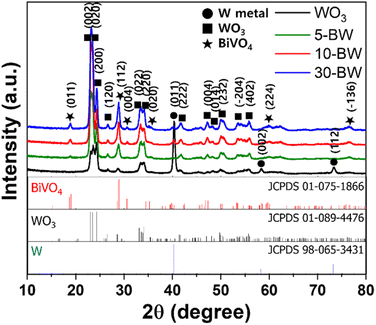
The crystalline phases of the WO3 nanocorals (5-BW, 10-BW, and 30-BW) were examined using XRD, as illustrated in Fig. 3. Peaks corresponding to W metal were observed at 40.2°, 58.2°, and 73.2° for the WO3 nanocorals, whereas only the 40.2° peak was observed for the BW samples. The XRD patterns of the WO3 nanocoral layer show peaks at 23.0°, 23.5°, 24.2°, 26.5°, 33.1°, 34.0°, 41.6°, 49.9°, and 55.7° indexed to the (0 0 2), (0 2 0), (2 0 0), (1 2 0), (0 2 2), (2 2 0), (2 2 2), (2 3 2), and (4 0 2) planes, respectively. The WO3 nanocorals exhibited well-crystallized monoclinic WO3 phases (JCPDS #089-4476).27,28 The XRD patterns of all the BW samples exhibited peaks at 18.9°, 28.9°, 30.5°, 40.2°, 60.0°, and 76.5° corresponding to the (0 1 1), (1 1 2), (0 0 4), (0 2 0), (1 2 1), (2 2 4), and (−1 3 6) planes, respectively, which are the monoclinic phases of BiVO4 (JCPDS #075-1866).29,30 Although 5-BW showed lower BiVO4 peak intensities at 18.9° and 30.5° owing to the quantity of BiVO4, the 10-BW and 30-BW peak intensities were similar. This indicates that 10 μL of the BiVO4 precursor is sufficient to form well-crystalized BiVO4 NPs that are to be used as photoanodes.
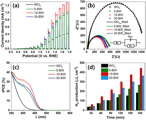
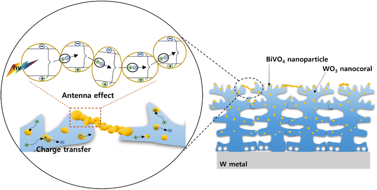
The chopped linear sweep voltammetry (LSV) curves with the PEC performance of 5-BW, 10-BW, and 30-BW are illustrated in Fig. 4a. Compared to the pristine WO3 nanocorals, all the BW photoanodes exhibited a higher photocurrent density, indicating that the heterostructural BW achieved an improved photocurrent density. The highest photocurrent density of 0.45 mA cm−2 at 1.23 V vs. RHE was obtained with the 10 μL spin-coated BiVO4/WO3 photoanode, and it was 2.4 times higher than that obtained for the WO3 nanocorals (0.19 mA cm−2 at 1.23 V vs. RHE). The BiVO4/WO3 photoanodes of 30-BW and 5-BW were followed to 0.42 and 0.35 mA cm−2 at 1.23 V vs. RHE. The 5-BW sample exhibited the lowest photocurrent density owing to the extremely small quantity of BiVO4 NPs on the WO3 layer. The fitted EIS Nyquist plots of the 5-BW, 10-BW, 30-BW, and WO3 nanocorals are depicted in Fig. 4b. In addition, the applied equivalent circuit consisting of the solution resistance (Rs), charge transfer resistance (Rct), and constant phase element (Qcpe) is shown in the inset. The sequence of charge transfer resistance values was in line with the photocurrent densities: 10-BW (457.3 Ω) < 30-BW (506.2 Ω) < 5-BW (561.1 Ω) < WO3 nanocorals (1450 Ω). After the PEC measurements, 10-BW showed an identical morphology and crystal structure (Fig. S3–S4†). In addition, the chemical composition of each element, except V, displayed identical intensities as illustrated in Fig. S5.† The decreased intensity of V is due to dissolution of V5+ ions, and the Bi peaks slightly shifted to higher binding energies owing to the strong influence of O bonding energy on Bi after the removal of V. However, this had negligible impact on the changes in performance. As presented in Fig. 4c, the linked BiVO4 NPs of 10-BW achieved the highest IPCE values of 39% at 360 nm and 30% at 410 nm. At 350 nm, the WO3 nanocorals, 5-BW, and 10-BW showed an approximate value of 40%, but 10-BW exhibited superior absorbance of light, even at a longer wavelength of 350 nm. The sequence of the IPCE values of the BW samples was 5-BW (36%), 30-BW (35%), and WO3 nanocorals (31%) at 360 nm; meanwhile, at 410 nm, the order changed to 30-BW (25%), 5-BW (23%), and WO3 nanocorals (4%). The two IPCE values of 5-BW and 30-BW were reversed at 372 nm, implying that 30-BW absorbed more visible light than 5-BW. Conversely, 5-BW can absorb more UV light than 30-BW. This indicates that a higher absorbance of visible light, instead of UV light, results in an improved PEC efficiency. The bandgaps evaluated using IPCE data are shown in Fig. S6.† Even though the amounts of the precursor were significantly different, the bandgaps of the WO3 nanocorals, 5-BW, 10-BW, and 30-BW were relatively similar, that is, 2.80, 2.54, 2.53, and 2.55 eV, respectively. PEC H2-production under solar light irradiation for 3 h is depicted in Fig. 4d. The H2 amounts of WO3 nanocorals, 5-BW, 10-BW, and 30-BW were 185.6, 267.6, 445.3, and 365.5 μL cm−2, respectively, and they linearly increased with increasing reaction time. H2 production is interrelated with photocurrent density, and high photocurrent density led to a high production rate; thus 10-BW obtained a higher H2 production rate of 123.0 μL h−1 cm−2 compared to 30-BW (86.3 μL h−1 cm−2) and 5-BW (33.6 μL h−1 cm−2), as shown in Fig. S7.† The faradaic efficiency for PEC H2-production using the optimal 10-BW was calculated to be 86%. In addition, the mixed structures of BiVO4 NPs and linked chains of NPs of 10-BW significantly improved the PEC efficiency by providing a charge-transfer pathway for electrons or holes to move easily toward WO3 or BiVO4 (Fig. 5). Moreover, the linked BiVO4 NPs can transfer photon energy from one NP to another, which is called the antenna effect31 resulting in high PEC activities. The linked BiVO4 NPs also connected one WO3 nanocoral to another during the migration of electron–hole pairs (excitons). Once the exciton is transferred to the WO3 nanocoral, the exciton is separated into both electron and hole, and the electron/hole transfer is activated.32 Then, each transferred electron migrates to the WO3 nanocoral, and the holes are transferred to the BiVO4 NPs. Furthermore, numerous generated excitons increase solar-to-hydrogen conversion efficiency,33 resulting in the generation of a high amount of H2.
3.2 Optimization of the BiVO4 precursor
To improve the quality of BiVO4, V concentrations in the BiVO4 precursor were controlled to be 0.15, 0.23, 0.3, and 0.6 M, and samples with these concentrations were labelled as V-0.15, V-0.23, V-0.3, and V-0.6, respectively, while the bismuth (Bi) concentration was fixed at 0.3 M. Each precursor was spin-coated on WO3 nanocorals with 10 μL optimized for PEC performance. Fig. 6 presents the different morphologies of the BW samples obtained with different V concentrations in the BiVO4 precursors. In the SEM image of V-0.15 (Fig. 6a), BiVO4 NPs were not observed, and the morphology was identical to that of the pristine WO3 nanocorals. BiVO4 NPs were rarely present in the SEM images of V-0.23, as illustrated in Fig. 6b. Linked BiVO4 NPs were observed only for V-0.3, as shown in Fig. 6c. The quantity of BiVO4 NPs increased with an increase in the V concentration from 0.23 M to 0.3 M. However, when the V concentration was increased to 0.6 M, some nanorods are suddenly obtained along with BiVO4 NPs as shown in Fig. 6d. The nanorods were composed of V and oxygen (O), as shown in Fig. S8.† Vanadium oxide nanorods were formed because of the high concentration of V.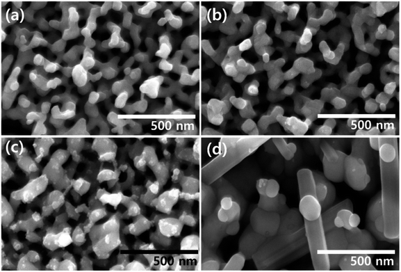 | ||
| Fig. 6 FE-SEM image of BiVO4/WO3 photoanodes depending on V concentration of the BiVO4 precursor; (a) 0.15, (b) 0.23, (c) 0.3, and (d) 0.6 M. | ||
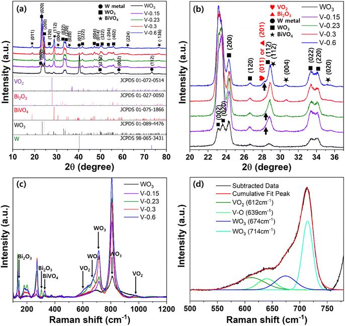
The XRD patterns of the V-controlled BiVO4/WO3 photoanodes are shown in Fig. 7a. The monoclinic phases of WO3 and BiVO4 exhibit the same patterns as those shown in Fig. 3. However, all the samples, except V-0.3, demonstrated a broad peak with a strong shoulder peak at approximately 28°, particularly V-0.6 (Fig. 7b). As shown in Fig. 6d, V-0.6 has vanadium oxide nanorods at the surface; thus, the peak at 27.89° was predicted to be of VO2 (JCPDS #072-0514),34 whereas the lack of V in the V-0.15 or V-0.23 samples could lead to the formation of bismuth oxides, which are responsible for the peak at 27.94° (JCPDS #027-0050).35 As the other peaks of VO2 or Bi2O3 overlapped with the WO3 or BiVO4 peaks, additional peaks were not investigated.
Raman scattering measurements were conducted to precisely characterize the V-controlled BiVO4 (Fig. 7c). The O–W–O stretching bands at 714 and 806 cm−1 allowed for the identification of monoclinic WO3.36 The peaks for V-0.15 were comparable to those of pristine WO3, as the BiVO4 NPs were rarely present on the surface of the WO3 nanocorals. After the formation of BiVO4, the remaining Bi in the BiVO4 precursor with V-0.23 formed bismuth oxide. Thus, the peak of Bi–O stretching mode of Bi2O3 at 304 cm−1 was only observed for V-0.23.37 Similarly, the residue of V in the BiVO4 precursor with V-0.6 formed vanadium oxide, VO2; thus, the corresponding peaks appeared at 612 and 988 cm−1, as shown in Fig. 6d.38,39 As a result, V-0.3 showed BiVO4 peaks at 326 and 374 cm−1 without any by-products, which were attributed to the asymmetric and symmetric deformation of VO43−.40 Therefore, 0.3 M of Bi and V is an optimal concentration as a BiVO4 precursor for fabrication of high-quality BiVO4 NPs.
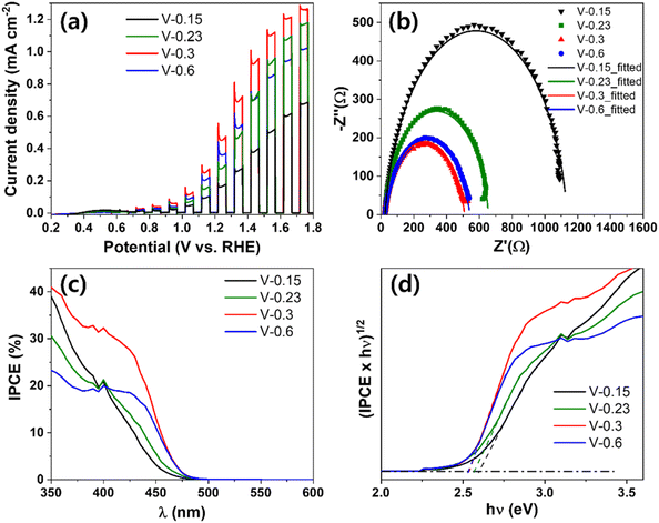
The PEC performances of different V-controlled BiVO4/WO3 photoanodes are shown in Fig. 8a. The optimal BW photoanode with V-0.3 showed the highest photocurrent density value of 0.45 mA cm−2 at 1.23 V vs. RHE. The V-0.6 and V-0.23 samples then followed with photocurrent densities of 0.36 and 0.27 mA cm−2 at 1.23 V vs. RHE, and 0.15 M showed an even lower photocurrent density of 0.16 mA cm−2 at 1.23 V vs. RHE compared to pristine WO3 nanocorals. Based on the photocurrent results, the sequence of charge transfer resistance should exhibit an opposite trend: the optimal BW photoanode of V-0.3 had the lowest resistance of 486.9 Ω followed by V-0.9 (518.1 Ω), V-0.44 (633.0 Ω), and V-0.3 (1110 Ω) as shown in Fig. 8b. The equivalent circuit and its components are the same as those shown in Fig. 4b. In Fig. 8c, the optimal BW photoanode (V-0.3) also shows the highest IPCE value of 29% at 420 nm. The order of the IPCE values for V-0.9 (19%), V-0.44 (15%), and V-0.3 (13%) at 420 nm is in line with the PEC results, proving that absorbing a high proportion of visible light remarkably enhances the PEC efficiency. For the evaluated bandgap from the IPCE values in Fig. 8d, the V-0.3 and V-0.44 samples showed bandgap values of 2.60 and 2.57 eV, and the V-0.3 and V-0.9 samples showed the same bandgap value of 2.53 eV. Nevertheless, V-0.9 showed a lower PEC performance than V-0.3 due to low IPCE efficiency in the range of 350 to 450 nm.
4. Conclusions
In summary, this study addressed the formation of heterostructured BiVO4 and WO3 with a mixed structure of NPs and linked BiVO4 NPs on WO3 nanocoral structures to enhance PEC performance. The linked BiVO4 NPs were simply constructed on anodic WO3 nanocorals by controlling the amount of the BiVO4 precursor to be 10 μL during spin-coating. This phenomenon was related to the hydrophilicity of the WO3 nanocorals, as the precursor amount on the WO3 nanocorals that could withstand a high speed rpm during spin-coating was important. Furthermore, the linked BiVO4 NPs/WO3 nanocoral heterostructure showed improved PEC performance, including photocurrent density, PEC H2 production, and IPCE, compared to the BiVO4 NPs/WO3 nanocoral heterostructure. The linked NPs on the WO3 nanocorals provided photogenerated electrons to move to the WO3 substrate and improved the charge carrier and charge separation via the antenna effect. Moreover, the NPs did not fully cover the WO3 nanocorals, and the nanocoral structures could harvest more light, which allowed for multiple light scattering. The optimized BiVO4 precursor concentration was 0.3 M of V and Bi, which formed the purest BiVO4 on the WO3 nanocorals without any by-product. When the V concentration was lower or higher than the Bi concentration, Bi2O3 or VO2 was formed along with BiVO4. Thus, the BW photoanode of the purist V-0.3 allowed realization of the highest photocurrent density and IPCE values of 0.45 mA cm−2 (at 1.23 V vs. RHE) and 29% (at 420 nm), respectively, and accordingly the lowest charge transfer resistance of 486.9 Ω.Conflicts of interest
There are no conflicts to declare.Acknowledgements
This work was supported by Inha University Research Grant.References
- Y. Park, K. J. McDonald and K.-S. Choi, Chem. Soc. Rev., 2013, 42, 2321–2337 RSC.
- J. Lee, M. Kim, Y.-T. Kim and J. Choi, Catal. Today, 2022, 403, 67–73 CrossRef CAS.
- K. Min, M. Kim, S. Min, H. Kim and S.-H. Baeck, Appl. Surf. Sci., 2023, 624, 157117 CrossRef CAS.
- M. Tayebi and B.-K. Lee, Renewable Sustainable Energy Rev., 2019, 111, 332–343 CrossRef CAS.
- V. S. Kumbhar, H. Lee, J. Lee and K. Lee, J. Colloid Interface Sci., 2019, 557, 478–487 CrossRef CAS PubMed.
- T. Kim, S. S. Patil and K. Lee, Electrochim. Acta, 2022, 432, 141213 CrossRef CAS.
- B. Jin, E. Jung, M. Ma, S. Kim, K. Zhang, J. I. Kim, Y. Son and J. H. Park, J. Mater. Chem. A, 2018, 6, 2585–2592 RSC.
- F. F. Abdi, L. Han, A. H. Smets, M. Zeman, B. Dam and R. van de Krol, Nat. Commun., 2013, 4, 2195 CrossRef PubMed.
- J. A. Seabold and K.-S. Choi, J. Am. Chem. Soc., 2012, 134, 2186–2192 CrossRef CAS PubMed.
- Y. Zhou, L. Zhang, L. Lin, B. R. Wygant, Y. Liu, Y. Zhu, Y. Zheng, C. B. Mullins, Y. Zhao, X. Zhang and G. Yu, Nano Lett., 2017, 17, 8012–8017 CrossRef CAS PubMed.
- X. Yao, D. Wang, X. Zhao, S. Ma, P. S. Bassi, G. Yang, W. Chen, Z. Chen and T. Sritharan, Energy Technol., 2018, 6, 100–109 CrossRef CAS.
- P. Lianos, Appl. Catal., B, 2017, 210, 235–254 CrossRef CAS.
- Y. Pihosh, I. Turkevych, K. Mawatari, T. Asai, T. Hisatomi, J. Uemura, M. Tosa, K. Shimamura, J. Kubota, K. Domen and T. Kitamori, Small, 2014, 10, 3692–3699 CrossRef CAS PubMed.
- S. S. Patil, J. Lee, E. Park, L. R. Nagappagari and K. Lee, ACS Appl. Energy Mater., 2021, 4, 13636–13645 CrossRef CAS.
- K. Fuku and K. Sayama, Chem. Commun., 2016, 52, 5406–5409 RSC.
- J. Wang, T. Zhou, Y. Zhang, L. Li, C. Zhou, J. Bai, J. Li, H. Zhu and B. Zhou, ACS Appl. Mater. Interfaces, 2022, 14, 45392–45402 CrossRef CAS PubMed.
- E. Park, S. S. Patil, H. Lee, V. S. Kumbhar and K. Lee, Nanoscale, 2021, 13, 16932–16941 RSC.
- B.-R. Huang, T.-C. Lin and Y.-M. Liu, Sol. Energy Mater. Sol. Cells, 2015, 133, 32–38 CrossRef CAS.
- G. Zheng, J. Wang, H. Liu, V. Murugadoss, G. Zu, H. Che, C. Lai, H. Li, T. Ding, Q. Gao and Z. Guo, Nanoscale, 2019, 11, 18968–18994 RSC.
- J. Su, L. Guo, N. Bao and C. A. Grimes, Nano Lett., 2011, 11, 1928–1933 CrossRef CAS.
- A. A. M. Ibrahim, I. Khan, N. Iqbal and A. Qurashi, Int. J. Hydrogen Energy, 2017, 42, 3423–3430 CrossRef CAS.
- Q. pan, H. Zhang, Y. Yang and C. Cheng, Small, 2019, 15, 1900924 CrossRef PubMed.
- P. Chatchai, S. Kishioka, Y. Murakami, A. Y. Nosaka and Y. Nosaka, Electrochim. Acta, 2010, 55, 592–596 CrossRef CAS.
- E. Park, T. Kim, J. Yoo and K. Lee, Inorg. Chim. Acta, 2023, 554, 121538 CrossRef CAS.
- L. Xia, J. Bai, J. Li, Q. Zeng, X. Li and B. Zhou, Appl. Catal., B, 2016, 183, 224–230 CrossRef CAS.
- J. Lee, S.-Y. Jung, V. S. Kumbhar, S. Uhm, H.-J. Kim and K. Lee, Catal. Today, 2021, 359, 50–56 CrossRef CAS.
- L. Zhang, H. Zhang, B. Wang, X. Huang, Y. Ye, R. Lei, W. Feng and P. Liu, Appl. Catal., B, 2019, 244, 529–535 CrossRef CAS.
- M. Saleem, M. F. Al-Kuhaili, S. M. A. Durrani, A. H. Y. Hendi, I. A. Bakhtiari and S. Ali, Int. J. Hydrogen Energy, 2015, 40, 12343–12351 CrossRef CAS.
- N. Ghazkoob, M. Zargar Shoushtari, I. Kazeminezhad and S. M. Lari Baghal, J. Alloys Compd., 2022, 900, 163467 CrossRef CAS.
- T. G. U. Ghobadi, A. Ghobadi, M. C. Soydan, M. B. Vishlaghi, S. Kaya, F. Karadas and E. Ozbay, ChemSusChem, 2020, 13, 2577–2588 CrossRef CAS PubMed.
- C.-y. Wang, C. Böttcher, D. W. Bahnemann and J. K. Dohrmann, J. Mater. Chem., 2003, 13, 2322–2329 RSC.
- G.-C. Fan, H. Zhu, Q. Shen, L. Han, M. Zhao, J.-R. Zhang and J.-J. Zhu, Chem. Commun., 2015, 51, 7023–7026 RSC.
- Y. Yan, R. W. Crisp, J. Gu, B. D. Chernomordik, G. F. Pach, A. R. Marshall, J. A. Turner and M. C. Beard, Nat. Energy, 2017, 2, 17052 CrossRef CAS.
- L. Zhao, L. Miao, C. Liu, C. Li, T. Asaka, Y. Kang, Y. Iwamoto, S. Tanemura, H. Gu and H. Su, Sci. Rep., 2014, 4, 7000 CrossRef CAS PubMed.
- S. Wang, P. Chen, Y. Bai, J.-H. Yun, G. Liu and L. Wang, Adv. Mater., 2018, 30, 1800486 CrossRef PubMed.
- F. Can, X. Courtois and D. Duprez, Catalysts, 2021, 11, 703 CrossRef CAS.
- M. G. Yañez-Cruz, M. Villanueva-Ibáñez, F. Méndez-Arriaga, C. A. Lucho-Constantino, M. d. l. Á. Hernández-Pérez, M. d. R. Ramírez-Vargas and M. A. Flores-González, J. Anal. Sci. Technol., 2022, 13, 52 CrossRef.
- I. Derkaoui, M. Khenfouch, I. Boukhoubza, M. Achehboune, R. Hatel, B. M. Mothudi, I. Zorkani, A. Jorio and M. Maaza, Appl. Phys. A, 2021, 127, 934 CrossRef CAS.
- M. Wan, M. Xiong, S. Tian, X. Chen, B. Li, X. Lu and X. Zhao, Materials, 2023, 16, 208 CrossRef CAS PubMed.
- M. R. d. S. Pelissari, N. F. Azevedo Neto, L. P. Camargo and L. H. Dall'Antonia, Electrocatalysis, 2021, 12, 211–224 CrossRef CAS.
Footnote |
| † Electronic supplementary information (ESI) available: FE-SEM, droplet schematics, bandgap, H2 production rate, and EDX data. See DOI: https://doi.org/10.1039/d3se01545a |
| This journal is © The Royal Society of Chemistry 2024 |


