The rise of quasi-2D Dion–Jacobson perovskites for photovoltaics
Jieyi
Chen
ab,
Zihao
Zhai
*a,
Qi
Liu
 a and
Huiqiong
Zhou
 *b
*b
aSchool of Materials Science and Engineering, Anhui Polytechnic University, Wuhu, 241000, P. R. China. E-mail: zhzhai@mail.ahpu.edu.cn
bCAS Key Laboratory of Nanosystem and Hierarchical Fabrication, National Center for Nanoscience and Technology, Beijing, 100190, P. R. China. E-mail: zhouhq@nanoctr.cn
First published on 14th September 2023
Abstract
With the advance of nanotechnology, the past couple of years have witnessed the fast development of quasi two-dimensional (2D) halide perovskites, which exhibit outstanding long-term stability against moisture and heat, compared with their three-dimensional (3D) counterparts. As one of the most common structures in 2D halide perovskites, quasi-2D Dion–Jacobson (DJ) perovskites show multiple-quantum-well structures with n layers of [BX6]4− octahedral inorganic sheets sandwiched by two layers of diammonium spacers, thus exhibiting superior structural stability due to the elimination of van der Waals gaps. Thanks to the achievement of high power conversion efficiency accompanied by impressive stability, quasi-2D DJ perovskite solar cells (PSCs) have recently drawn extensive attention in the field. This review first introduces the fundamental understanding of quasi-2D DJ halide perovskites, including their superior stability, high exciton binding energy, and compositional flexibility and tunable properties. We then summarize detailed strategies to prepare high-quality quasi-2D DJ perovskites for PSCs, encompassing compositional engineering, solvent engineering, additive addition, and annealing processes. Moreover, the surface/interface modification and 2D–3D hybrid perovskite heterojunction are also discussed, for providing strategies to optimize the fabrication of quasi-2D DJ PSCs. Lastly, current challenges and perspectives toward the future development of quasi-2D DJ perovskites for photovoltaics are outlined.
1. Introduction
Organic–inorganic halide perovskite nanocrystals have been applied as light absorption sensitizers for dye-sensitized solar cells since 2009.1 From then on, perovskite light absorption materials, as new stars in the photovoltaic device community, have drawn significant attention due to their outstanding optoelectrical properties that involve a high absorption coefficient, long carrier diffusion length and tunable bandgap.2–5 The past decade has witnessed a fast-growth period in power conversion efficiency (PCE) for perovskite solar cells (PSCs), which has been boosted from only 3.8%1 to a certified 25.73%,6 making them comparable to commercial silicon solar cells7. Among the efficient PSCs, typical three-dimensional (3D) organic–inorganic halide PSCs are the bellwether that usually breaks the PSC efficiency record.8–10 However, the inferior stability of traditional 3D perovskites hinders them from realizing large-scale applications.In particular, 3D perovskites have the formula ABX3, where the structures comprise corner-shared [BX6]4− octahedra with an A+ cation that occupies the voids (shown in Fig. 1a).11 In the structure of ABX3, the A site is CH3NH3+ (MA+), NH2CHNH2+ (FA+) or Cs+, while the B site is Pb2+ or Sn2+, and the X site is a halide anion such as I−, Br− or Cl−. MAPbI3 perovskites are sensitive to high temperature and humidity, under which the perovskites should degrade into CH3NH2, HI and PbI2.12–14 For FAPbI3 perovskites, the photoactive α-FAPbI3 phase easily transforms into an undesired δ-FAPbI3 phase.15,16 Moreover, even all-inorganic CsPbI3 perovskites with superior thermal stability exhibit phase instability in a humid environment.17–19 To address these issues, bulkier hydrophobic organic cations are introduced to partly substitute the small and hygroscopic organic cations for the formation of two-dimensional (2D) perovskites (including 2D or quasi-2D perovskites) with enhanced stability (Fig. 1a).20–24 The 2D perovskites are conceptually achieved by cutting along the 〈100〉, 〈110〉, or 〈111〉 crystallographic directions of the 3D perovskite structures (Fig. 1b).25,26 Among the 2D perovskites, the 〈100〉-oriented perovskites are mostly employed,11 since there are a larger pool of organic cations that can be used to form the 〈100〉-oriented perovskites. As for 〈110〉-oriented variants, they are intrinsically distorted and unstable, which often leads to the formation of self-trapped excitons. The 〈111〉-oriented perovskites are metal-site deficient and hard to stabilize, so that only a couple of examples of these structures exist.27 By introducing different types of organic amines, 〈100〉-oriented layered hybrid perovskites can be mainly divided into three types, which involve a Ruddlesden–Popper (RP) phase,28–31 Dion–Jacobson (DJ) phase32–35 and an alternating cation in the interlayer space (ACI) phase36–38 (Fig. 1c). The full names and abbreviations of organic spacer cations mentioned in this review are listed in Table 1.
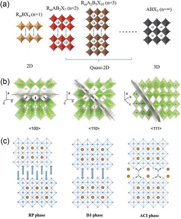 | ||
| Fig. 1 (a) Schematics of 2D, quasi-2D and 3D perovskite structures. Reproduced with permission from ref. 23. Copyright 2022 Elsevier. (b) Structure derivation of three kinds of layered perovskites with an inserted spacer cation along the 〈100〉, 〈110〉, and 〈111〉 directions of the 3D perovskites. Reproduced with permission from ref. 26. Copyright 2021 Wiley-VCH. (c) Crystal structures of RP, DJ, and ACI phase quasi-2D perovskites. Reproduced with permission from ref. 23. Copyright 2022 Elsevier. | ||
| Full name | Abbreviation |
|---|---|
| 3-(Aminomethyl)piperidinium | 3AMP2+ |
| 4-(Aminomethyl)piperidinium | 4AMP2+ |
| 4-(2-Aminoethyl)pyridinium | 4AEPy2+ |
| 1,4-Butanediammonium | BDA2+ |
| 1,6-Hexamethylenediammonium | HDA2+ |
| 1,8-Octanediammonium | ODA2+ |
| 1,3-Propane-diammonium | PDA2+ |
| 1,5-Pentamethylenediammonium | PeDA2+ |
| 1,4-Phenylenedimethanammonium | PDMA2+ |
| Butylammonium | BA+ |
| 1,4-Benzenedimethanamonium | BzDA2+ |
| 3-(Aminomethyl)pyridinium | 3AMPY2+ |
| 4-(Aminomethyl)pyridinium | 4AMPY2+ |
| 2,2′-Disulfanediylbis(ethan-1-ammonium) | DSDEA2+ |
| 2,3,5,6-Tetrafluoro-1,4-benzenedimethanammonium | TFBDA2+ |
| 2,3,5,6-Tetrafluoro-1,4-phenylenedimethanammonium | 4F-PDMA2+ |
| Bithiophene dimethylammonium | BThDMA2+ |
| trans-1,4-Cyclohexanediammonium | CHDA2+ |
| 2,5-Thiophenedimethylammonium | ThDMA2+ |
| Thieno[3,2-b]thiophene-2,5-diyldimethanaminium | TTDMA2+ |
| N,N-Dimethyl-1,3-propanediammonium | DMePDA2+ |
| p-Xylylene diammonium | XDA2+ |
| p-Phenylenediammonium | PPD2+ |
| p-Xylylenediammonium | PXD2+ |
| Phenylenediethylammonium | PEDA2+ |
Generally, the quasi-2D RP and DJ phase perovskites can be expressed as (A′)m(A)n−1BnX3n+1, where A′ represents monovalent cations for the RP phase (m = 2) or divalent cations for the DJ phase (m = 1) and n represents the number of inorganic layers. While for quasi-2D ACI phase perovskites, the formula is A′(A)nBnX3n+1, where A′ is a guanidinium (GA+) cation. The DJ phase perovskite is focused on in this review. DJ PSCs evolved recently in 2018 when 3-(aminomethyl)piperidinium (3AMP2+) and 4-(aminomethyl)piperidinium (4AMP2+) cation based DJ PSCs were reported, though an efficiency of only 7.32% was obtained.33 However, a significant rise in efficiency from 7.32% to 18.82% for DJ perovskite PSCs was witnessed within a few years.32 Typically, van der Waals gaps exist in quasi-2D RP perovskites, while the neighboring inorganic slabs are bridged by diammonium spacers in quasi-2D DJ perovskites without these gaps.33 Thus, compared to RP perovskites, DJ perovskites usually show superiority in stability and charge transport. Moreover, it was reported that a 1D phase forms on exposure of a DJ perovskite precursor to humidity, and the hydration process is partly reversible by annealing, which implies the potential possibility for regaining performance loss in 3D/2D architectures.39
Though some reviews on the progress of RP perovskites have been reported, the related advances on DJ PSCs are rarely reviewed. Herein, we focus on DJ phase perovskites and PSCs. We first introduce the fundamental understanding of DJ halide perovskites, covering their superior stability, high exciton binding energy (Eb), as well as compositional flexibility and tunable properties. Then, detailed strategies for preparing high-quality quasi-2D DJ perovskite films are summarized, encompassing compositional engineering, solvent engineering, additives addition, and annealing processes. In addition, surface/interface modification and the 2D–3D hybrid perovskite heterojunction are also discussed, which provide promising strategies to optimize the fabrication technique for DJ PSCs. Finally, we highlight the existing challenges and summarize perspectives on the future development of quasi-2D DJ perovskites for photovoltaics.
2. Fundamental understanding of DJ halide perovskites
2.1 Superior stability
2D DJ perovskite crystals are multiple-quantum-well (MQW) structures in which n layers of [BX6]4− octahedral inorganic slabs are sandwiched by two layers of diammonium spacers. Specifically, the inorganic layers act as “wells”, whereas the organic spacers act as “barriers”40–42 (Fig. 2a). Owing to the inclusion of a single divalent cation, DJ halide perovskites exhibit a (0, 0) shift with large cations, where one layer is stacked strictly on top of the others,33,36,43 different to 2D RP halide perovskites (Fig. 2b). However, dividing most structures into DJ or RP phases is unquantifiable. Recently, a layer shift factor (LSF) was introduced by Tarasov et al. for univocal classification and quantitative comparison of layered hybrid halide perovskites. They revealed that the different LSF values correspond to the existence of different conformations of interlayer cations, which correlates with the penetration level of organic cations into inorganic layers.44 In general, the outstanding stability of 2D DJ perovskites can be mainly ascribed to their high formation energy, suppressed ion migration, and high hydrophobicity.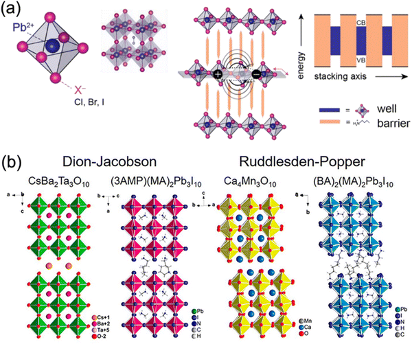 | ||
| Fig. 2 (a) Structures of lead halide perovskites exhibiting dimensional tunability and serving as natural quantum well systems for the 2D structure. Reproduced with permission from ref. 42. Copyright 2019 Elsevier. (b) Comparison of the DJ and RP phases of oxide and halide perovskites. Reproduced with permission from ref. 33. Copyright 2018 American Chemical Society. | ||
The organic spacer plays a crucial role in stabilizing the crystal lattice. The ionic and covalent bonds, along with intermolecular forces, contribute to the high stability of quasi-2D perovskites. Thus, a higher energy is required to interrupt the interaction between large spacer cations in 2D perovskites than the MA+ cations in 3D analogs (Fig. 3a).45 Besides, as studied by density functional theory (DFT), Sargent et al. clarified that the formation energy of quasi-2D perovskites decreases as the n values increase. Additionally, quasi-2D DJ perovskites with various organic spacers show different formation energies. For instance, Wei and co-workers reported that (4AEPy)PbI4 (4AEPy2+, 4-(2-aminoethyl)pyridinium) presents a higher formation energy than (BDA)PbI4 (BDA2+, 1,4-butanediamonium) and (HDA)PbI4 (HDA2+, 1,6-hexamethylenediammonium), which could benefit the stability of the devices.46
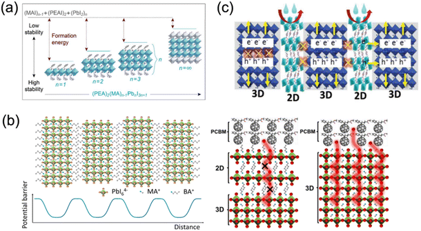 | ||
| Fig. 3 (a) The relevance of formation energy, stability and n values of quasi-2D perovskites. Reproduced with permission from ref. 45. Copyright 2016 American Chemical Society. (b) Suppressed ion migration by organic spacer “barriers” in 2D perovskites. Reproduced with permission from ref. 51 and 52. Copyright 2017, 2018 American Chemical Society. (c) Incorporated long organic cations in perovskite crystal functioning as a blocking layer against moisture and oxygen. Reproduced with permission from ref. 55. Copyright 2018 Wiley-VCH. | ||
Recent studies have revealed that ion migration (MA+, Pb2+, I−) plays a significant role in the hysteresis and degradation in hybrid perovskite materials, and thus influences the long-term stability of PSCs.47–49 An appreciable number of ions should move along the field direction under an electric or light field, creating vacancies/excess defects that act as charge recombination centers in perovskite films. However, the aforementioned organic spacer “barriers” in 2D perovskites can limit the ion migration to a specific space, which ultimately enhances the stability and suppresses the hysteretic effect,50–52 as demonstrated in Fig. 3b. Li and co-workers deposited a 1,8-octanediammonium (ODA2+) based quasi-2D DJ perovskite on a 3D perovskite to construct 2D–3D PSCs. The devices exhibited decreased hysteresis, which was attributed to the suppressed ion migration, as well as the enhanced charge transport between active layer and hole transport layer (HTL).53 Liu and co-workers synthesized a 2D BDAPbI4 single crystal and reported a reduced ion migration for BDAPbI4 compared to MAPbI3, which was mainly ascribed to the strong hydrogen bonds between the organic cations and inorganic slabs in BDAPbI4. The low defect density and weak ion migration were reported to contribute to the superior detection performance of BDAPbI4.54
The hydrophobicity of large spacer cations such as organic aromatic or aliphatic alkyl ammonium in layered perovskites protects the perovskite lattice from moisture (Fig. 3c).55 However, large organic cations with inferior electrical conductivity isolate the conductive inorganic layers, leading to quantum confinement effects. Therefore, the length of spacers is expected to be not too long to guarantee the electrical performance. For instance, Lee et al. found that the quantum confinement no longer dominated in quasi-2D perovskites after replacing the large monoammonium organic cation butylammonium (BA+) with the small diammonium organic cation 1,3-propane-diammonium (PDA2+), since this reduced the distance between inorganic frameworks and led to considerable enhancement in charge transport. The efficiency of encapsulated PDA-based quasi-2D PSCs still retained 90% of the original efficiency after 1000 h.34 Furthermore, quasi-2D perovskites based on organic cations such as BDA2+,56 1,5-pentamethylenediammonium (PeDA2+),57 3AMP2+,20 1,4-phenylenedimethanammonium (PDMA2+),58etc., were also investigated, which showed impressive moisture stability and/or thermal stability.
2.2 High exciton binding energy
The hybrid structure causes quantum confinement within inorganic layers and exhibits a quantum well (QW) structure.42 The organic dielectric spacers and inorganic slabs in 2D perovskites serve as “barriers” and “wells”, respectively. The exciton confinement of 2D perovskites will be intensified by the organic spacer barrier, ultimately leading to a high Eb.59,60 Theoretically, the Eb of inorganic semiconductor quantum wells in a low-dimensional perovskite is calculated using the following equations:61,62 | (1) |
 | (2) |
 | (3) |
 | (4) |
| α = 3 − γe−Lw/2aB | (5) |
In quasi-2D perovskites, the dielectric constants of organic cations are smaller than those of inorganic slabs, which further increases the Eb. The Eb is 5–60 meV for 3D perovskites, while that for 2D perovskites is much higher, approximately 100–500 meV.64 The higher Eb values of 2D perovskites make them suitable for photonic applications as efficient lasers,65,66 light-emitting diodes,67,68 and photodetectors.69,70 However, a high Eb value for 2D perovskites will hinder their practical exploitation in light harvesters. Due to the fact that the quantum and dielectric confinement increase while dimensions of the perovskite crystal decrease, the 2D perovskites exhibit suboptimal optoelectronic behavior compared to their 3D counterparts. According to eqn (1)–(5), the Eb value can be regulated through tuning the composition, as well as the n values.
Xu and co-workers found that a (BDA)PbI4 perovskite has a much lower Eb value (≈142 meV) than a (BA)2PbI4 perovskite (≈435 meV). It was explained that the short ligand length between inorganic frameworks in DJ phase perovskites contributes to a stronger interlayer interaction of excitons than that of RP phase perovskites (Fig. 4a).71 Additionally, a flat energy landscape generally exists in DJ perovskites, which is due to their narrow thickness distribution of QWs, and thus contributes to fast charge separation and extraction.72 Huang and co-workers investigated various DJ phase perovskites with PDA2+, BDA2+, PeDA2+, and HDA2+ organic ammonium cations, respectively, discovering that the QW barrier thickness was affected by the chain length of bulky organic spacers. They also found that the QW thickness played a vital role in crystal orientation and QW distribution of DJ phase perovskites. Compared to those perovskites with PeDA and HDA organic spacers, PDA and BDA based quasi-2D perovskites exhibit better orientation and more uniform QW distribution, resulting in a longer carrier diffusion length and higher charge mobility (Fig. 4b).73
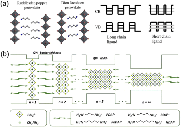 | ||
| Fig. 4 (a) Structure diagram of RP and DJ phase quasi-2D perovskites and a schematic illustration of the exciton coupling effect of the MQW structure for ligands with different lengths. Reproduced with permission from ref. 71. Copyright 2020 Wiley-VCH. (b) The QW structure of DJ perovskite films based on different organic diammoniums. Reproduced with permission from ref. 73. Copyright 2019 Wiley-VCH. | ||
A high Eb value makes the photogenerated carriers generate in the form of excitons instead of free electrons/holes in quasi-2D perovskites. Therefore, the key point for achieving high PCEs for quasi-2D PSCs is to aim at the physicochemical distinction between organic spacers and inorganic frameworks. Tailoring organic cations and regulating n values are effective strategies to inhibit the dielectric and quantum confinement effects.
2.3 Superior compositional flexibility and tunable properties
Quasi-2D DJ perovskites exhibit the structure (A′)(A)n−1BnX3n+1, where the n value is the inorganic framework layers in the perovskite crystal structure. Investigation has manifested that the properties of quasi-2D DJ perovskites are greatly related to n values (Fig. 5a–d).33,58,74 Generally, the bandgaps of quasi-2D DJ perovskites reduce when the n values increase. The formation energy of quasi-2D DJ perovskites decreases as the n value increases, indicating that low-dimensional perovskites exhibit better stability compared to their high-dimensional counterparts. The increase in n value for DJ perovskites results in a redshift in absorbance and PL spectra (Fig. 5e). Also, the n values have significant effects on the morphology and structure of the perovskite films. Etgar et al. discovered that BzDA-based (BzDA2+, 1,4-benzenedimethanamonium) DJ quasi-2D perovskites show nonoriented platelet crystals when n = 1, whereas those with higher n values exhibit dense and defined crystals.75 Liang and co-workers reported that confined structures (showing excitonic absorption peaks) were obtained in PDMA-based perovskites with small n values, while nonconfined structures were acquired in analogues with large n values. The quantum confinement effect was suppressed for the nonconfined structures, which as a result led to efficient charge splitting and charge transport (Fig. 5f and g).76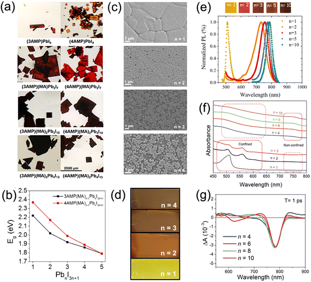 | ||
| Fig. 5 (a) Optical images and (b) summary of bandgaps of 3AMP and 4AMP based quasi-2D perovskite crystals with different n values. Reproduced with permission from ref. 33. Copyright 2018 American Chemical Society. (c) SEM images and (d) photographs of perovskite films based on different (PDMA)FAn−1PbnI3n+1 compositions (n = 1–4). Reproduced with permission from ref. 58. Copyright 2019 American Chemical Society. (e) PL data and photographs of BzDA based perovskite films with various n values. Reproduced with permission from ref. 75. Copyright 2019 American Chemical Society. (f) Optical absorption and (g) TA spectra of perovskite films based on PDMA2+ organic cations. Reproduced with permission from ref. 76. Copyright 2019 Wiley-VCH. | ||
Additionally, the selection of large organic cations, halogen anions, and metal cations also have significant impacts on the optoelectronic properties of DJ perovskites. Kanatzidis et al. reported the first examples of 2D DJ hybrid perovskites with 3AMP2+ and 4AMP2+ organic cations. They found that owing to the different position of the functional group for the organic cations 3AMP2+ and 4AMP2+, the perovskites showed diverse optical and electronic properties, which resulted in a smaller bandgap and enhanced charge transport for 3AMP compared with 4AMP (Fig. 6a and b).33 They also investigated the CH2NH3+ group position of the 4-(aminomethyl)pyridinium (4AMPY2+) and 3-(aminomethyl)pyridinium (3AMPY2+) organic cations, discovering that the rigidity of the cation was increased while the dielectric mismatch was decreased for aromatic spacers, as compared to the aliphatic cation AMP2+. This showed a significant influence on the structural and optical properties of the perovskites (Fig. 6c–e).74 It was demonstrated that different chain lengths of bulky organic ammonium spacers allowed the control of QW distribution.73 Substitution of MA with Cs in DJ perovskites for enhanced stability has been investigated by several groups.77,78 Li and co-workers reported that a 5% Cs doped DJ quasi-2D perovskite presented better crystallographic orientation and a higher carrier lifetime in contrast to intrinsic ones (Fig. 6f–h).78 Furthermore, replacement of Pb with Sn allows a suitable bandgap, a high carrier mobility, and a low Eb for quasi-2D DJ perovskites. Research studies on Sn or Sn/Pb based DJ phase perovskites with 3AMP,79 4-(aminomethyl)pyridinium (4AP2+),80 and BDA81 organic spacers have also been reported recently.
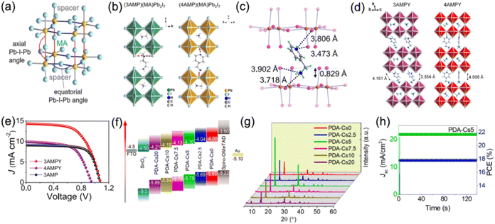 | ||
| Fig. 6 (a) Schematic diagram of axial and equatorial Pb–I–Pb angles for 3AMP and 4AMP based DJ perovskites. (b) Structures of (3AMP)(MA)Pb2I7 and (4AMP)(MA)Pb2I7. Reproduced with permission from ref. 33. Copyright 2018 American Chemical Society. (c) Distance between organic cations and inorganic frameworks for (3AMPY)(MA)Pb2I7. (d) Structures of (3AMPY)(MA)Pb2I7 and (4AMPY)(MA)Pb2I7. (e) J–V results of 3AMPY, 4AMPY and 3AMP based DJ PSCs. Reproduced with permission from ref. 74. Copyright 2019 American Chemical Society. (f) Energy band alignment and (g) XRD patterns of (PDA)Csx(MA)3−xPb4I13 films. (h) Stabilized PCE and Jsc values of the champion (PDA)Cs0.05(MA)2.95Pb4I13 device. Reproduced with permission from ref. 78. Copyright 2022 Elsevier. | ||
3. Methods for improving the quality of DJ perovskite films
3.1 Compositional engineering
The molecular composition of DJ perovskites has an important impact on film formation. Thus, compositional engineering is a facile and feasible approach to effectively regulate the film quality of DJ perovskites through regulating n values, organic spacer A-sites and B-site cations.As previously mentioned, increasing the stacking number of inorganic slabs in quasi-2D perovskites is an effective method to weaken the dielectric confinement effect and broaden electronic bands, which can ultimately decrease Eb and allow adjusting of the optoelectronic properties. In general, the average thickness of inorganic slabs is decided by the layer numbers, which is expressed by the n value. Thus, the n value is an important factor that determines the optoelectrical properties of DJ phase quasi-2D perovskites, which as a result influences the absorption and conductivity/mobility, as well as the stability. Generally, as the n values increase, the electronic bands broaden, and thus result in weakened quantum confinement and a smaller bandgap.74,82 Changes in the color of DJ perovskites with various n values can be observed, which usually appear yellow for n = 1, red for n = 2, dark brown for n = 3, 4, and finally black when n = ∞.58,75 The absorption spectra of DJ perovskites typically display an exitonic peak for a typical 2D phase, which gradually disappears as the n value increases. In addition, apparent Stokes shifts can be observed in the PL spectra for DJ perovskites with n ≥ 2.58,74,75 According to the research of Blancon et al., these peak shifts were explained by the presence of “edge states” that feature in layered 2D perovskite materials.83 Furthermore, DJ perovskite films with different n values normally present diverse surface morphology. Liang and co-workers discovered that PDMA-based DJ perovskite films showed varied surface morphology from a rough surface with disordered rod-shape crystal grains, to a plain and dense surface, and to a surface with random and excessive large grains, as the n values increased.76 So far, highly-efficient DJ phase PSCs have been typically reported with n > 3.56,57,84
The close interlayer distance in DJ phase quasi-2D perovskites enables weak exciton confinement and efficient charge separation/transfer. Up to now, many research studies have focused on the design of a bulky molecular structure, so as to enhance the interlayer coupling and optimize the optoelectronic properties.85,86 DJ perovskites with different spacer cations for PSC fabrication and their impacts on photovoltaic performance are displayed in Table 2. The previous study primarily focused on dielectric constant, flexibility, and the functional group of organic spacers, which have been supposed to play an important role in affecting the kinetics and phase distribution.87,88 Due to their simple chain structure, DJ phase perovskites with aliphatic alkyl ammonium were reported first. Huang et al. synthesized DJ perovskite films with different bulky organic chain lengths, finding that PDA and BDA based quasi-2D perovskites showed better orientation and more uniform QW distribution than those with PeDA and HDA organic spacers (Fig. 7a).73 Moreover, the longer exciton lifetime of PDA and BDA based films compared to others allowed a smooth bandgap transition. Consequently, DJ quasi-2D PSCs based on PDA and BDA showed high efficiencies of 14.16% and 16.38%, respectively. Lee et al.34 and Li et al.35 discovered that DJ quasi-2D PSCs exhibited higher efficiency and stability than RP phase analogs. It is speculated that disulfide bonds could capture an electron and form a stable two-center three-electron bond, which serves as a relay station for electron transfer reactions.89 Accordingly, 2,2′-disulfanediylbis(ethan-1-ammonium) (DSDEA2+) with an S–S unit was used as an organic cation in DJ quasi-2D perovskites, which was found to favor the crystallinity, oriented growth, and charge transport of perovskite films, as compared to the perovskite with HDA2+ used as the organic spacer (Fig. 7b–d).86
| Organic cations | DJ perovskite (DJP) | n | Bandgap (eV) | Device configuration | PCE (%) |
|---|---|---|---|---|---|
| PDA2+ | (PDA)(MA)n−1PbnI3n+134 | 2 | 1.96 | ITO/PEDOT:PSS/DJP/C60/BCP/Ag | 3.8 |
| 3 | — | 9.0 | |||
| 4 | 1.63 | 13.0 | |||
| (PDA)(MA)n−1PbnI3n+135 | 1 | 2.46 | FTO/TiO2/DJP/spiro-OMeTAD/Au | 0.3 | |
| 2 | 1.77 | 1.27 | |||
| 3 | 1.69 | 9.1 | |||
| 4 | 1.63 | 13.3 | |||
| (PDA)(MA)2Pb3I1096 | 3 | — | ITO/PEDOT:PSS/DJP/PCBM/BCP/Cu | 11.27 | |
| (PDA)(FA)n−1PbnI3n+197 | 2 | 1.94 | ITO/SnO2/DJP/spiro-OMeTAD/Ag | 2.45 | |
| 3 | 1.81 | 8.45 | |||
| 4 | 1.75 | 13.8 | |||
| BDA2+ | BDAPbI498 | 5 | 2.37 | FTO/TiO2/DJP/spiro-OMeTAD/Ag | 1.08 |
| BDAPbI499 | 1 | 2.37 | FTO/TiO2/DJP/spiro-OMeTAD/Au | 1.10 | |
| (BDA)(MA)4Pb5I16100 | 5 | — | ITO/PEDOT:PSS/DJP/PCBM/LiF/Ag | 17.91 | |
| (BDA)(MA)4Pb5I1673 | 5 | — | ITO/PEDOT:PSS/DJP/PCBM/LiF/Au | 16.38 | |
| (BDA)(Cs0.1FA0.9)4Pb5I1677 | 5 | — | FTO/cp-TiO2/mp-TiO2/DJP/Spiro-OMeTAD/Au | 18.2 | |
| (BDA)(FA)2Sn3I10101 | 3 | 1.34 | ITO/PEDOT:PSS/DJP/PCBM/Ag | 6.43 | |
| (BDA)(MA)4Pb5X16102 | 5 | 1.59 | ITO/PTAA/DJP/PCBM/BCP/Ag | 14.53 | |
| (BDA)(FA)4Pb5I16−xBrx103 | 5 | 1.59 | ITO/SnO2/DJP/spiro-OMeTAD/Au | 16.75 | |
| (BDA)0.8(PEA2)0.2MA4Pb5X16104 | 1 | 1.63 | ITO/PEDOT:PSS/DJP/PCBM/BCP/Au | 17.21 | |
| (BDA)(MA0.07FA0.93)4Pb5I16105 | 5 | — | ITO/SnO2/Perovskite/Spiro-OMeTAD/Au | 19.55 | |
| (BDA)(MA)4Pb5X1656 | 5 | 1.63 | ITO/PTAA/DJP/C60/BCP/Ag | 17.61 | |
| PeDA2+ | (PeDA)(MA)4Pb5X1673 | 5 | 1.65 | ITO/PEDOT:PSS/PVK/PC60B/LiF/Al | 12.95 |
| (PeDA)(MA)4Pb5X1657 | 5 | — | ITO/PTAA/DJP/C60/BCP/Ag | 18.41 | |
| HDA2+ | HDAPbI498 | 1 | 2.44 | FTO/TiO2/DJP/spiro-OMeTAD/Ag | 0.59 |
| (HDA)(MA)4Pb5I1673 | 5 | — | ITO/PEDOT:PSS/PVK/PC60B/LiF/Al | 10.55 | |
| PDMA2+ | (PDMA)(FA)n−1PbnI3n+158 | 1 | 2.42 | FTO/TiO2/DJP/spiro-OMeTAD/Au | 0.91 |
| 2 | — | 2.91 | |||
| 3 | — | 6.46 | |||
| 4 | 1.51 | 7.11 | |||
| (PDMA)(MA)5Pb6I1976 | 6 | — | ITO/PEDOT:PSS/DJP/PCBM/Bphen/Ag | 10.86 | |
| (PDMA)(Cs0.05MA0.15FA0.8)9Pb10(I0.93Br0.07)3175 | 10 | — | FTO/TiO2/DJP/spiro-OMeTAD/Au | 15.60 | |
| (PDMA)(MA)3Pb4I13106 | 4 | — | FTO/TiO2/DJP/spiro-OMeTAD/Au | 15.81 | |
| 4F-PDMA2+ | (4F-PDMA)(MA)3Pb4I13107 | 4 | 1.40 | ITO/PEDOT:PSS/DJP/PCBM/BCP/Ag | 17.37 |
| 3AMP2+ | (3AMP)(MA)3Pb4I1320 | 4 | 1.57 | FTO/PEDOT:PSS/DJP/C60/BCP/Ag | 7.02 |
| (3AMP)(MA0.85FA0.15)3Pb4I1320 | 4 | 1.53 | 9.30 | ||
| (3AMP)(MA0.75FA0.25)3Pb4I1320 | 4 | 1.48 | 12.04 | ||
| (3AMP)(MA0.75FA0.25)3Pb4I13108 | 4 | — | ITO/NiOx/PTAA/DJP/PCBM/BCP/Ag | 18.67 | |
| (3AMP)(MA0.75FA0.25)3Pb4I13109 | 4 | — | ITO/PTAA/PFN-Br/DJP/PCBM/BCP/Ag | 16.25 | |
| (3AMP)(MA)n−1PbnI3n+133 | 3 | 1.92 | FTO/PEDOT:PSS/DJP/C60/BCP/Ag | 2.02 | |
| 4 | 1.87 | 7.32 | |||
| 4AMP2+ | (4AMP)(MA)n−1PbnI3n+133 | 3 | 1.99 | FTO/PEDOT:PSS/DJP/C60/BCP/Ag | 3.67 |
| 4 | 1.89 | 4.24 | |||
| (4AMP)(FA)3Sn4I13110 | 4 | 1.47 | FTO/TiO2/ZrO2/DJP/Carbon | 4.22 | |
| (4AMP)(MA)2Pb3I10111 | 3 | — | ITO/PEDOT:PSS/DJPe/PCBM/BCP/Al | 18.3 | |
| 3AMPY2+ | (3AMPY)(MA)3Pb4I13,74 | 4 | 1.85 | FTO/PEDOT:PSS/DJP/C60/BCP/Ag | 9.20 |
| 4AMPY2+ | (4AMPY)(MA)3Pb4I13,74 | 4 | 1.89 | 5.69 | |
| ODA2+ | ODAPbI499 | 1 | — | FTO/TiO2/DJP/spiro-OMeTAD/Ag | 2.55 |
| CHDA2+ | (CHDA)(MA)3Pb4I13112 | 4 | — | FTO/SnO2/DJP/spiro-OMeTAD/Au | 15.01 |
| ThDMA2+ | (ThDMA)(MA)4Pb5I16113 | 5 | 1.60 | ITO/PEDOT:PSS/DJP/PCBM/BCP/Ag | 15.75 |
| TTDMA2+ | (TTDMA)(MA)3Pb4I1332 | 4 | — | ITO/PEDOT:PSS/DJP/PCBM/BCP/Ag | 18.82 |
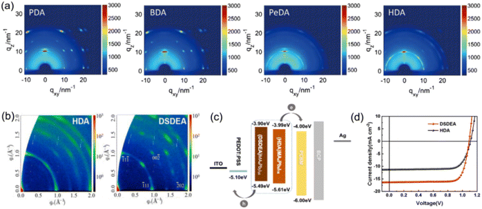 | ||
| Fig. 7 (a) GIWAXS patterns of PDA2+, BDA2+, PeDA2+, and HDA2+ based perovskite films. Reproduced with permission from ref. 73. Copyright 2019 Wiley-VCH. (b) GIWAXS patterns of HDA2+ and DSDEA2+ based perovskite films. (c) Energy band alignment and (d) J–V results of HDA2+ and DSDEA2+ based PSCs. Reproduced with permission from ref. 86. Copyright 2022 Elsevier. | ||
Besides aliphatic chains, aliphatic rings have also been applied in the organic cation. Kanatzidis et al. studied DJ perovskites with 3AMP2+ and 4AMP2+ organic cations, finding that the position of the –CH2NH3+ group indeed had an impact on the crystal structure by forming different hydrogen-bonding modes that resulted in the distortion of the Pb–I–Pb angle. Compared to DJ perovskites with 4AMP2+ organic cations, the 3AMP2+ based films exhibited a narrower bandgap as well as enhanced charge transport on account of their less distorted structure.33 However, unlike the aliphatic cation, the delocalized π electrons in the aromatic cation improved the dielectric confinement and led to a smaller Eb, which benefited the films with superior carrier transport performance. Thus, Kanatzidis et al. thereafter synthesized DJ perovskite films with 3AMPY2+ and 4AMPY2+ organic cations, concluding that the replacement of the aliphatic ring (AMP) by aromatic spacers led to the increased rigidity of the cations, reduced interlayer spacing, and decreased dielectric mismatch.74 Zheng et al. designed and synthesized a new fluorinated diammonium cation (TFBDA2+, 2,3,5,6-tetrafluoro-1,4-benzenedimethanammonium) for quasi-2D DJ PSCs (Fig. 8a).90 The PL spectra and TRPL results indicated that the TFBDA-based perovskite films possess lower trap density and higher mobility, as compared to unfluorinated counterparts (Fig. 8b and c). The energy level alignments in Fig. 8d demonstrate that the TFBDA-based perovskite is able to realize efficient electron transfer.
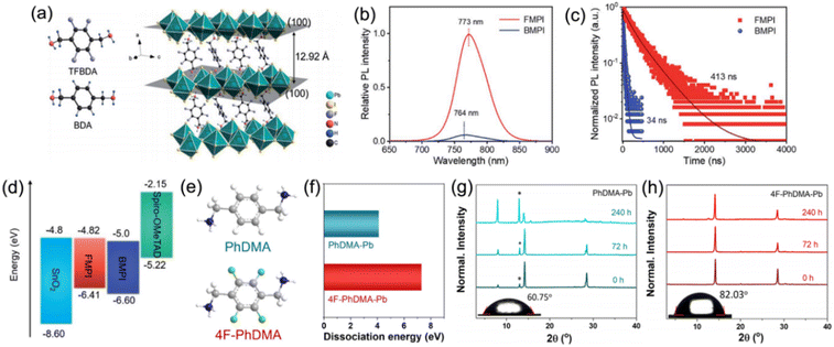 | ||
| Fig. 8 (a) Chemical structures of TFBDA2+ and BDA2+ cations, and the crystal structure of (TFBDA)PbI4. (b) PL spectra and (c) PL decay of TFBDA2+ and BDA2+ based perovskite films. (d) Energy band alignment of TFBDA2+ and BDA2+ based quasi-2D PSCs. The TFBDA based perovskite is named FMPI, while the BDA based perovskite is named BMPI. Reproduced with permission from ref. 90. Copyright 2021 Royal Society of Chemistry. (e) Chemical structure of PDMA2+ and 4F-PDMA2+ cations. (f) Dissociation energy of PDMA-Pb and 4F-PDMA-Pb based perovskites. XRD patterns of (g) PDMA-Pb and (h) 4F-PDMA-Pb based quasi-2D perovskite films exposed to an ambient atmosphere. Reproduced with permission from ref. 88. Copyright 2021 American Chemical Society. | ||
A multifluorinated aromatic spacer (4F-PDMA2+, 2,3,5,6-tetrafluoro-1,4-phenylenedimethanammonium) was applied for DJ quasi-2D perovskites by Liu and co-workers.88 The chemical structure of PDMA2+ and 4F-PDMA are given in Fig. 8e. They discovered that ascribed to the multiple noncovalent interactions, the 4F-PDMA based quasi-2D DJ perovskites showed high dissociation energy, leading to the increased structure stability of devices (Fig. 8f). The much higher stability against moisture for perovskite films with 4F-PDMA organic spacers than that for PDMA based films was attributed to their improved hydrophobicity that was confirmed by contact angle measurements (Fig. 8g and h). Eventually, the optimized 4F-PDMA based DJ PSC exhibited an efficiency of 16.62%, that is, higher than those of devices using unfluorinated organic spacers. Grätzel and co-workers explored the effects of humidity on (PDMA)PbI4 DJ perovskite composition. They found that structural transformation of disrupting the layered perovskite structure occurred when exposed to a humid environment and that the hydration-induced process was partially reversible.39 They also studied the role of spacer length for 1,4-phenylenediammonium (PPD2+), PDMA2+, and 1,4-phenylenediethylammonium (PEDA2+) based DJ perovskites and concluded that long alkyl chains and bromide compositions could enhance the optical properties and stability of the perovskites.91 Besides, they also confirmed that compared to PDMA-based perovskites, perovskites with perfluorinated PDMA2+ cations presented enhanced stability against moisture.92
Bithiophene dimethylammonium (BThDMA2+) was also applied in DJ quasi-2D perovskites.93 It was discovered that compared to aliphatic ODA2+ cation based perovskites, stronger orbital interactions exist in BThDMA2+ based perovskites, which contribute to crystal growth and improved charge mobility. Consequently, the optimal (BThDMA)MA4Pb5I16 PSC showed an excellent PCE of 18.1%. Moreover, it was found by Guo et al. that the rigidity of organic cations in 2D DJ perovskites could induce co-adaptation of organic diammonium cations and inorganic [PbI6]4− octahedra to stabilize the 2D structure. A cyclic 1,4-cyclohexanedimethanammonium (CyDMA2+) based 2D perovskite was shown to exhibit better structural stability compared to PDMA- and HDA-based 2D perovskites.94
Moreover, 2D perovskite systems based on bifunctional organic spacers are not guaranteed to form a DJ phase layered structure, which can often form other lower-dimensional 1D phases.95 For instance, Grätzel and co-workers discovered that perovskites based on PDA exhibit a 1D structure instead of forming a well-defined layered structure, whereas extending the alkyl chains to PDMA and PDEA rendered them to more easily form a layered structure.91 This was supposed to be ascribed to the lack of flexibility and low penetration depth into the neighboring slabs for the PDA spacer.
Additionally, tailoring the A-site or B-site cations of quasi-2D DJ perovskites is another strategy to improve the properties of perovskite films. Grätzel and co-workers reported FA containing quasi-2D DJ perovskites with the bifunctional organic spacer PDMA2+. The (PDMA)FA2Pb3I10 PSC achieved an efficiency of >7% and exhibited outstanding stability after being exposed to air for over two months.58 They also investigated (PDMA)FAn−1PbnI3n+1 (n = 1–3) DJ perovskites to reveal their underlying structural and photophysical properties. They discovered that compositions with n ≥ 2 were difficult to form owing to the improved formation energy as the thickness of the inorganic slabs increased. This research illustrates the high photoconductivity and long carrier lifetime for the n ≥ 2 phase that is promising for photovoltaic applications.114 A series of (PDA)FAn−1PbnI3n+1 perovskite films synthesized by Chen et al. showed higher thermal decomposition activation energy than their MA-containing analogues. The (PDA)FA3Pb4I13 PSCs exhibited high thermal stability and retained 86% of the original efficiency after being stored at 85 °C for 1000 h (Fig. 9a and b).97 Similar results were also reported by Xu et al., which showed that the FA-based DJ films presented higher film quality and better stability compared to MA-based ones (Fig. 9c and d).85 The phase segregation for the (BDA)FA2Pb3I10 perovskite was significantly suppressed, indicating the improved humidity stability of the FA-based films, as confirmed in Fig. 9e. The FA-based perovskite device exhibited better photovoltaic properties than the MA-based device (Fig. 9f). Moreover, Zhao et al. reported that introducing an EDAPbI4 (EDA, ethylenediamine) 2D DJ perovskite into α-CsPbI3 perovskites enabled their superior phase stability and a highly reproducible efficiency of 11.8%.115 Jin et al. embedded fluorinated aromatic cations in CsPbI3 to form DJ phase quasi-2D perovskites. They found that the fluorinated 2-fluorobenzene-1,4-diamine (F-PDA) based (F-PDA)Csn−1PbnI3n+1 exhibited a reduced Eb and enhanced charge transfer compared to the 1,4-diaminobenzene (PDA) based (PDA)Csn−1PbnI3n+1. Eventually, a PCE of over 15% was achieved by (F-PDA)Cs3Pb4I13 PSCs with markedly improved stability than their 3D counterparts.116
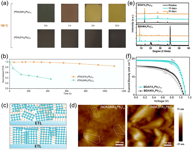 | ||
| Fig. 9 (a) Photographs of MA-based and FA-based perovskite films at different intervals during thermal stress at 150 °C. (b) Thermal stability tests at 85 °C for MA- and FA-based PSCs. Reproduced with permission from ref. 97. Copyright 2020 Wiley-VCH. (c) Schematic of the crystal orientation for (BDA)(MA)2Pb3I10 (the top) and (BDA)(FA)2Pb3I10 (the bottom) DJ perovskite films. (d) AFM images and (e) XRD patterns of (BDA)(MA)2Pb3I10 and (BDA)(FA)2Pb3I10 perovskite films. (f) J–V curves of champion (BDA)(FA)2Pb3I10 and (BDA)(MA)2Pb3I10 PSCs under AM1.5G illumination. Reproduced with permission from ref. 85. Copyright 2023 Wiley-VCH. | ||
The toxicity of Pb-based perovskites impedes their commercialization.117 Therefore, Sn or mixed Pb/Sn is commonly employed to replace the B site of typical 2D DJ perovskites, since Sn and Pb belong to the same group in the periodic table. Moreover, the low Eb and high carrier mobility of Sn-based perovskites make Sn an ideal substitute element for Pb.118 However, Sn-based perovskites are fairly unstable when exposed to water and oxygen, which impedes their further development. Li and co-workers introduced a 4AP2+ cation to construct the 2D DJ perovskite 4APSnX4.80 They found that high temperature was able to provide a charge transfer channel and further enhance the charge transfer efficiency.
Furthermore, the structural and optoelectronic properties can also be tuned through incorporating mixed A-site and/or A′-cations. For instance, Kanatzidis et al. synthesized new 2D DJ (3AMP)a(4AMP)1−a(FA)b(MA)1−bPb2Br7 perovskites, finding that the fractions of 4AMP and FA had significant impacts on Pb–Br–Pb angles, which thus affected the structural and optical properties of the perovskites.119
When designing the compositions of DJ phase perovskites, it is important to focus on the size, flexibility, dielectric constant, and functional group of the organic spacers and the n values, which have significant impacts on the crystallization kinetics and phase distribution. Doping elements at the A-site and/or introducing mixed cations at the B-site results in the achievement of the desired optoelectronic properties through manipulating the crystal structure, carrier dynamics, and stability.
3.2 Solvent control
Solvent engineering has become a crucial strategy to optimize crystallization kinetics and film quality since it is able to control the process of nucleation and crystallization.120 Generally, organic spacers in a quasi-2D perovskite tend to be parallel to substrates (out-of-plane orientation) through a self-assembly formation process. A binary solvent of N,N-dimethylformamide (DMF) and dimethyl sulfoxide (DMSO) has become a popular solvent adopted in a precursor solution to prepare high-quality RP phase quasi-2D perovskite films,121–123 since it is able to overcome the issue of downward vertical growth orientation.124 Similarly, the binary solvent approach is also applied in the synthesis of DJ phase perovskite films.32,106,112Kanatzidis et al. adopted a mixed solvent of DMF, DMSO, and hydroiodic acid (HI) to synthesize 3AMP-based perovskite films.20 Compared to perovskite films synthesized in pure DMF solvent, those prepared in a mixed DMF/DMSO solvent exhibited a smoother and more compact surface (Fig. 10a). In addition, the addition of HI to the precursor solution contributed to higher crystalline quality and preferred orientation (Fig. 10b), yielding high reproducibility and enhanced performance for devices. Liu et al. discovered that with the introduction of DMSO, ThDMA-based (ThDMA2+, 2,5-thiophenedimethylammonium) quasi-2D perovskite films exhibited a larger grain size and reduced trap-state density than those without DMSO (Fig. 10c and d).113 Guo et al. demonstrated that solvent composition has significant impacts on regulating the crystallization kinetics of DJ phase perovskites.125 The XRD patterns of freshly coated films in Fig. 10e exhibit three distinct diffraction peaks for films with pure DMF and a binary DMF:DMSO solvent, suggesting the formation of an intermediate phase. The XRD patterns of the intermediate film with binary and ternary solvents show several peaks at low angles, indicating the formation of a precursor adduct, while that with only DMF exhibits only perovskite peaks. The incorporation of 1-methyl-2-pyrrolidinone (NMP) into the DMF:DMSO binary solvent, namely an NMP-based ternary solvent, slowed the crystallization rate due to the strong coordinating interaction with precursor ingredients, and resulted in enhanced crystallinity (Fig. 10f). Ternary-solvent-based champion DJ PSCs exhibited a stabilized efficiency of 16.19%.
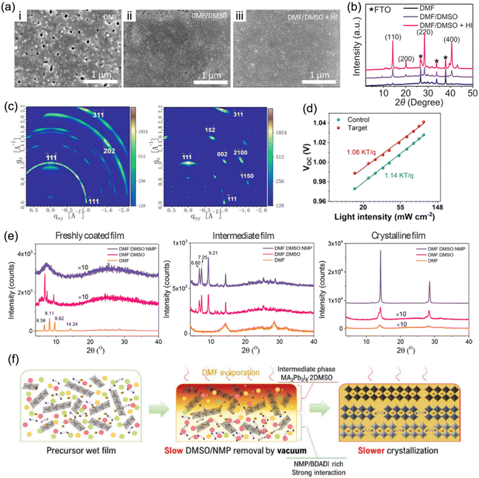 | ||
| Fig. 10 (a) SEM images and (b) XRD patterns of (3AMP)(MA0.75FA0.25)3Pb4I13 films processed in DMF, DMF/DMSO, and DMF/DMSO/HI solvents. Reproduced with permission from ref. 20. Copyright 2019 Wiley-VCH. (c) GIWAXS data of the ThDMA-based DJ perovskite films: control (with DMF solvent, left) and target films (with optimized DMF/DMSO binary solvent, right). (d) Relation of the Vocversus light intensity for ThDMA-based DJ perovskite control and target films. Reproduced with permission from ref. 113. Copyright 2020 American Chemistry Society. (e) XRD patterns of perovskite films synthesized with different solvents. (f) Schematics of vacuum-assisted crystallization processes for DJ perovskites synthesized with the ternary solvent DMF:DMSO:NMP. Reproduced with permission from ref. 125. Copyright 2022 Wiley-VCH. | ||
To further improve the film crystallinity, ion liquid methylammonium acetate (MAAc), which is supposed to cooperate with DMSO to jointly regulate the film quality of quasi-2D perovskites, was also utilized as an effective solvent. Huang's group first prepared DJ phase perovskite films with MAAc solvent and fabricated photovoltaic devices that reached a high PCE of 16.38%.73 Zhou et al. studied the influence of MAAc solvent on film formation and the trap states of a quasi-2D DJ perovskite. They discovered that the nucleation process during spin-coating was slowed with MAAc solvent (Fig. 11a). As demonstrated in Fig. 11b, MAAc provided extra coordination, and thus slowed the nucleation process of the films. Due to the high viscosity of MAAc, the nucleation process and continuous crystal growth was slowed down because of the slow rate of solvent removal. The films prepared with MAAc exhibited preferential orientation (Fig. 11c). Eventually, the PeDA-based perovskite films presented out-of-plane oriented crystallization and their devices achieved a high efficiency of 18.41%.57 Furthermore, Li et al. reported a simple and eco-friendly method using ethyl acetate (EA) as an anti-solvent to synthesize MA-free and DMePDA-based (DMePDA2+, N,N-dimethyl-1,3-propanediammonium) DJ perovskite films. Due to the rapid extraction of solvents and interaction between Pb2+ and the carbonyl group in the solvent, the perovskite films showed homogeneous phase distribution and decreased surface defect density. Finally, the champion PSC reached a high efficiency of 18.86%.84
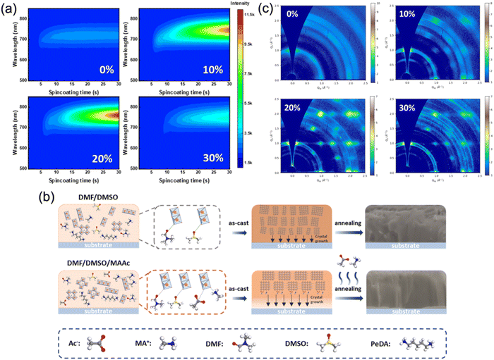 | ||
| Fig. 11 (a) In situ PL spectra and (b) GIWAXS patterns of the (PeDA)(MA)3Pb4I13 synthesized with different MAAc ratios. (c) Schematic of the film formation process for films synthesized with and without MAAc. Reproduced with permission from ref. 57. Copyright 2022 American Chemical Society. | ||
Organic solvents such as DMF and DMSO enable the precursors to form a Lewis acid–base intermediate adduct and benefit the crystallization process through determining the nucleation and growth of perovskite crystals. In terms of ionic liquid solvents, they provide a strong hydrogen bond network and electrostatic environment, which contribute to dissolving and stabilizing the solution.
3.3 Functional additives addition
Compared to 3D perovskites, the DJ phase quasi-2D counterparts show inferior device performance that mainly arises from undesirable charge transport efficiency. This can be ascribed to the large Eb and random crystal orientation in DJ phase perovskites. To date, additive engineering has been considered to be an effective approach to overcome these issues and promote optoelectronic performance and device stability.Jen et al. employed NH4SCN additives to facilitate the growth of a (BDA)(MA)4Pb5I16 perovskite.102 The XRD patterns in Fig. 12a present that the crystal orientation of the perovskite was influenced by NH4SCN. The GIWAXS patterns in Fig. 12b exhibit the isotropic ring of the (101) plane for a film without addictive, implying the randomly orientation of the crystals in the perovskite film, while sharp and discrete Bragg spots can be seen in films with NH4SCN additives. The orientation of the (101) plane could be regulated from randomly to perpendicularly oriented with respect to substrate through increasing the amounts of NH4SCN additives (Fig. 12c). Wu and co-worker also applied SCN− (MASCN) as an additive to prepare high-quality 3AMP-based quasi-2D perovskite films and achieved a high PCE of 16.25%.109 Satapathi and co-workers also reported DJ quasi-2D (XDA)MA3Pb4I13 (XDA2+, p-xylylene diammonium) perovskites processed with NH4SCN additive and their devices obtained a high PCE of 17.05%.126 In their investigation, the apparently increased decay lifetime indicated suppressed non-radiative recombination in films with NH4SCN (Fig. 12d). The Vocversus light intensity curves show decreased slope for devices with NH4SCN (Fig. 12e). Fig. 12f demonstrates an increased water contact angle for the film with NH4SCN compared to that without additive, which indicated the high hydrophobicity for perovskite films with NH4SCN additive.
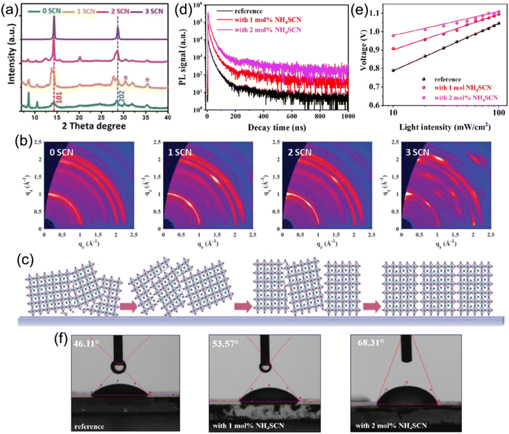 | ||
| Fig. 12 (a) XRD patterns of (BDA)(MA)4Pb5I16 perovskite films with various SCN− additives. (b) GIWAXS patterns of (BDA)(MA)4Pb5I16 perovskite films with an incidence angle of 1.0°. (c) Schematic of the orientation evolution for perovskites with NH4SCN additives. Reproduced with permission from ref. 102. Copyright 2019 Wiley-VCH. (d) TRPL graphs of (XDA)MA3Pb4I13 perovskite films and (e) Vocvs. the light intensity measurement of (XDA)MA3Pb4I13 PSCs without additive (reference), with 1 mol% NH4SCN and 2 mol% NH4SCN. (f) Water contact angles of (XDA)MA3Pb4I13 perovskite films without additive (reference), with 1 mol% NH4SCN and 2 mol% NH4SCN. Reproduced with permission from ref. 126. Copyright 2022 American Chemical Society. | ||
The NH4+ and SCN− ions are able to regulate the growth rate and nucleation of perovskite crystal grains, and thus contribute to an improvement in film quality and device stability. On the one hand, small-sized NH4+ anions can diffuse easily into the [PbI6]4− octahedra, which promotes heterogeneous nucleation and eventually results in a reduction in the defects in perovskites.127 On the other hand, the SCN− in the precursor solution may replace I− and bond to [PbI6]4− owing to the strong interaction between Pb2+ and S/N atoms in SCN−.128 The perovskite colloids with negatively-charged SCN− are mutually repulsive in the precursor, which leads to the potential dimensional control of colloids.
Moreover, MACl additive was also adopted to adjust the crystallization process of DJ 2D perovskites based on various organic cations such as p-phenylenediammonium (PPD2+), p-xylylenediammonium (PXD2+), and PDA2+.96 The perovskite films without MACl additive exhibited a series of diffraction rings, which indicated the random orientation of crystal grains, while the samples with MACl additive presented highly concentrated diffraction spots that indicated well-ordered crystal orientation (Fig. 13a). In a previous study on RP perovskites, it was clarified that the PbI2-DMF-based solvated phase (PDS) precipitated first in solution and promoted the formation of 3D perovskites at the surface, followed by the oriented crystal growth of RP phases with 3D perovskites as a template.129 Similarly, the XRD results (Fig. 13b) suggested that the PDS was dominated by an (MA)2(DMF)2Pb3I8 intermediate phase, while the MACl additive was precipitated. Fig. 13c shows a schematic diagram of the crystallization process for a DJ phase quasi-2D perovskite with MACl additive. The MACl additive restricted the precipitation of PDS in solution, which was beneficial to the formation of PDS on the solution surface and the downward growth of DJ perovskites, and thus resulted in a dominant out-of-plane crystal orientation. Consequently, the PDS engineering for (PXD)(MA)2Pb3I10 perovskites led to a significant enhancement in the PCE of devices from 1.2% to 15.6%. Min et al. also employed thiourea and MACl to synergistically facilitate the crystallization process, which resulted in a smooth and dense surface morphology, and improved phase purity.130 Chen et al. reported well-oriented PDA-based DJ perovskite films synthesized using FACl additive.97Fig. 13d depicts the XRD patterns of PDA-based perovskite films. It reveals that the non-perovskite phase and PbI2 component were effectively removed and led to well-oriented perovskite films through introducing FACl as an additive. Fig. 13e shows a schematic illustration of the mechanism of perovskite film growth with FACl additives. Firstly, at high temperature, the unstable δ-phase FAPbI3 transforms into an α-phase, and the Cl-containing intermediates are converted to perovskites via the exchange of I− and Cl−. Subsequently, FACl evaporation occurs. After that, the PDA2+ organic cations are attached to the inorganic slabs via hydrogen bonding, which modulates the perovskite orientation. Finally, the film synthesized with FACl additive exhibits a preferred orientation.
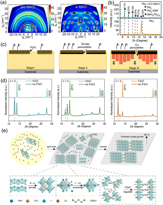 | ||
| Fig. 13 (a) GIWAXS images of (PXD)(MA)2Pb3I10 perovskite films without and with MACl additive. (b) XRD curves of perovskite films without and with MACl additive. (c) Schematic diagram of the crystallization process for DJ phase perovskite films with MACl additive. Reproduced with permission from ref. 96. Copyright 2020 Wiley-VCH. (d) XRD patterns of perovskite films with different n values prepared with and without FACl additive. (e) Schematic illustration of the mechanism of perovskite film growth with FACl additive. Reproduced with permission from ref. 97. Copyright 2020 Wiley-VCH. | ||
It is a general belief that the addition of Cl− facilitates the formation of Cl-containing intermediates, which present as a transient state. The Cl-containing intermediates are transformed to a preferable perovskite phase through I/Cl ion exchange and the Cl− is effectively removed after the annealing process because of its volatile nature. Eventually, Cl− additives contribute to the highly preferred perovskite crystal direction that is perpendicular with respect to the substrate.
3.4 Temperature and annealing process management
To date, the common approach used to prepare DJ perovskite films for PSCs has been to spin-coat a precursor solution in one step, followed by thermal annealing at over 100 °C. The management of the temperature and annealing process is critical for preparing high-quality quasi-2D DJ perovskite films. Hence, the following methods demonstrated in this part have been extensively applied to facilitate the temperature and annealing process when synthesizing quasi-2D DJ perovskite films.Loo et al. have reported a general post-deposition strategy, namely solvent-vapor annealing (SVA), to induce vertical orientation growth of DJ phase perovskite films.77 After annealing for 1 h, the spin-coated perovskite films were put onto a hot plate at a temperature of 100 °C, and covered by a glass jar wherein N2 was bubbled through an isopropanol (IPA) reservoir to carry IPA vapor into the annealing jar (Fig. 14a). The GIWAXS patterns show that the isotropic diffraction rings of the reference films were substituted with discrete Bragg spots after SVA treatment, suggesting the preferred orientation (Fig. 14b). It was found that the IPA vapor plasticized quasi-2D perovskites and offered sufficient mobility for the surface to reorient (Fig. 14c). This preferred vertical orientation resulted in decreased bulk and surface defects, and improved the charge transport at the perovskite/electron transport layer (ETL) interface. Eventually, the optimal device after SVA treatment achieved a certified efficiency of 18.00%. Liu et al. presented an in-depth understanding about the effects on the film formation of (PDMA)(MA)3Pb4I13 perovskites by using different solution-casting approaches.106 They deposited the precursor films at room temperature (control), by antisolvent dripping, and by hot-casting approaches, respectively. The in situ absorption spectra shown in Fig. 14d indicate the minimum nucleation density for the control sample, which involved a necessary high-temperature annealing process for perovskite crystallization. Unlike the unfavorable indirect phase transformation for the control films, the processes for films fabricated by antisolvent dripping or hot-casting approaches exhibited fast evaporation of solvent and suppressed intermediate phases, as well as facilitating the crystal nucleation. The antisolvent sample exhibited random orientation, while the hot-casting sample showed preferred orientation. Consequently, the hot-casting film exhibited a smaller trap density and a higher carrier mobility than the other films. Zhou and co-workers reported a thermally-induced crystallization method through processing (BDA)(MA)4Pb5I16 DJ perovskite films with thermal treatments. They screened the annealing temperature and found that films with enhanced crystallinity and compact structures were obtained at an annealing temperature of 120 °C.56 It was discovered that the enhancement in the device performance was mainly ascribed to efficient charge generation, suppressed nonradiative recombination, and reduced interfacial charge accumulation. Eventually, the champion PSC achieved a high Voc of 1.21 V and an optimal efficiency exceeding 17.6%. Moreover, Chou et al. used an intense near-infrared lamp as an annealing energy source and found that this resulted in nonisothermal (NIT) crystallization of PDMA-based perovskites, in contrast with isothermal (IT) crystallization on a hotplate. Due to the two-step crystallization in the NIT process, the perovskite films exhibited better morphology, more efficient charge transport, and oblique orientation compared with those synthesized by conventional IT crystallization.131
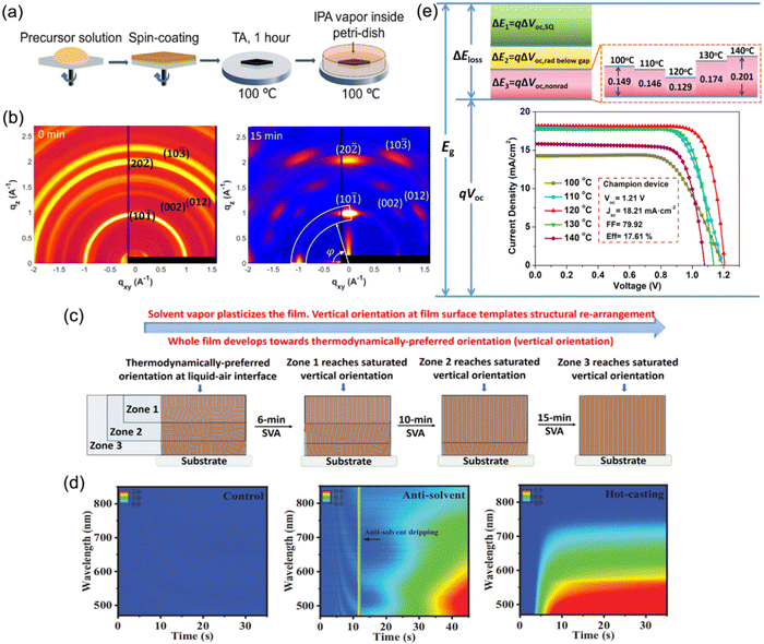 | ||
| Fig. 14 (a) Schematic diagram of the post-deposition processing of 2D perovskite films. (b) GIWAXS patterns of quasi-2D perovskite films without (0 min) and with (15 min) SVA treatment. (c) Illustration of the reorientation process during SVA. Reproduced with permission from ref. 77. Copyright 2020 American Chemical Society. (d) In situ absorption spectra during spin-coating processes for the control, antisolvent, and hot-casting films. Reproduced with permission from ref. 106. Copyright 2021 Wiley-VCH. (e) Schematic of energy loss for (BDA)(MA)4Pb5I16 PSCs optimized using a thermally-assisted crystallization strategy. The inset shows the J–V curves of devices processed at different annealing temperatures. Reproduced with permission from ref. 56. Copyright 2022 Wiley-VCH. | ||
The temperature and annealing process assisted by hot-casting, solvent-vapor or near-infrared irradiation essentially influence the nucleation process of perovskite films, which has an impact on the size of the crystal nuclei and growth rate of the grains. This process can be used to optimize the morphology, defect density, and crystal orientation of DJ phase perovskite films.
4. Optimizing the fabrication techniques of DJ PSCs
4.1 Surface/interface modification
Carrier nonradiative recombination, which is responsible for inferior charge extraction and collection, originates from the bulk and interface. Nonradiative recombination hinders quasi-2D PSCs from developing towards efficient and stable devices. To date, many kinds of approaches, which include compositional engineering, solvent control, and additive engineering, have been studied to optimize the carrier transport, extraction and collection for DJ perovskites. In addition, surface and interface modification in DJ phase quasi-2D PSCs have also been investigated.Chen and co-workers proposed a gradient Br doping (GBD) process to regulate the interfacial energy band alignment in DJ phase PSCs.103 FABr (dissolved in IPA) was spin-coated on (BDA)FA4Pb5I16 films to form a new perovskite composition (BDA)FA4Pb5I16−xBrx with GBD through an I− and Br− exchange reaction (Fig. 15a). The corresponding energy level diagram demonstrates that the target perovskite film possessed a higher conduction band minimum (CBM) and valence band maximum (VBM) than the control sample, which resulted in the formation of a staggered-gap heterointerface that was beneficial to charge extraction and collection (Fig. 15a). The transient photocurrent (TPC) and transient photovoltage (TPV) results suggested increased charge extraction and transfer as well as suppressed nonradiative recombination for the target sample (Fig. 15c and d). Through GBD optimization, the devices finally achieved a high efficiency of 16.75%. Chen and Wu et al. demonstrated a strategy for combining pre-annealing and merged annealing (PMA) to effectively construct a merged 3AMP-base perovskite/PCBM interface, which promoted the contact between the perovskite absorber and ETL, and contributed to defect restriction and charge transport.108Fig. 15e presents the three different fabrication processes for a 3AMP-base perovskite film coated with PCBM. Moreover, a secondary anti-solvent method was reported by Zhang and co-workers for further passivating surface defects.105Fig. 15f shows a schematic diagram of the common and secondary anti-solvent processes for (BDA)(MA0.07FA0.93)4Pb5I16 perovskite preparation. The results of positron annihilation spectroscopy (PAS) demonstrate that the shape parameter (S parameter) near the top surface was higher in the control (Fig. 15g). However, the S parameter decreased evidently after secondary surface passivation treatment, which indicated a smaller trap density and proved that the secondary anti-solvent method could effectively passivate the surface defects. In addition, the phase distribution after secondary anti-solvent treatment exhibited a gradient signature, which facilitated both the light absorption and charge transportation in the 2D PSCs (Fig. 15h). The modified BDA-based PSC finally achieved a PCE of 19.55%.
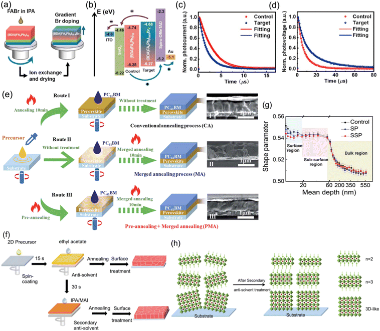 | ||
| Fig. 15 (a) Schematic diagram of the GBD strategy for the preparation of a gradient (BDA)FA4Pb5I16−xBrx perovskite. (b) Energy level diagram for control and target devices. (c) TPC and (d) TPV results for control and target devices. Reproduced with permission from ref. 103. Copyright 2021 Elsevier. (e) Schematic diagram of different annealing processes for the preparation of PCBM-coated (3AMP)(MA0.75FA0.25)3Pb4I13 perovskite films. Reproduced with permission from ref. 108. Copyright 2021 Royal Society of Chemistry. (f) Schematic diagram of the common and secondary anti-solvent processes for (BDA)(MA0.07FA0.93)4Pb5I16 perovskite preparation. (g) PAS results of control, surface passivation (SP), and secondary surface passivation (SSP) perovskite films. (h) Schematic illustration of the phase distribution in (BDA)(MA0.07FA0.93)4Pb5I16 perovskite films after secondary anti-solvent treatment. Reproduced with permission from ref. 105. Copyright 2022 Wiley-VCH. | ||
Surface/interface modification for perovskite films has been proved to greatly influence the charge extraction and surface trap density. The optimization of the surface of perovskite films and interface of the perovskite/charge transporting layer are effective methods to improve device performance.
4.2 2D–3D hybrid perovskite heterojunction
2D perovskite capping layers grown on top of light-absorbing 3D perovskite layers to form 2D–3D hybrid heterojunctions are able to promote device performance with suppressed ion migration and improved long-term stability. In this structure, the 3D perovskites are responsible for high efficiencies owing to their outstanding optoelectronic properties, while the 2D perovskites protect the underlying layer from moisture and further improve the PCE as a result of their passivation effect and gradient energy level. Generally, the chemical composition, ratio of spacer cations, and processing procedures all significantly influence the structural and photoelectric properties of 2D–3D heterojunctions.Guo et al. reported DJ 2D–3D perovskites synthesized through depositing an ODA2+-based 2D phase layer onto a 3D phase layer with excess PbI2 (Fig. 16a).132 The 2D perovskite exhibited a intermediate highest occupied molecular orbital (HOMO) level, which favored hole transfer and extraction. Meanwhile, its lowest occupied molecular orbital (LUMO) level was able to restrict electron transfer from the 3D perovskite to the HTL, and therefore reduced the charge recombination (Fig. 16b). Eventually, an optimal PCE of 21.6% was obtained. Moreover, BDA-based and EDBE-based DJ 2D perovskites, respectively, were also used to construct 2D–3D devices, which exhibited enhanced stability and yielded high conversion efficiency.133,134 Moreover, a localized DJ 2D–3D heterostructure (L2D–3DH) was also demonstrated.135 In comparison with the traditional 2D–3D structure, the L2D–3DH barely hindered the charge transfer at the perovskite/HTL interface owing to the partial coverage of the 2D phase. Moreover, the L2D–3DH devices exhibited better stable performance than pure 3D devices. The L2D–3DH films treated with over 0.4 mg ml−1 BDAI2 still maintained their black color after storage in air for days without encapsulation, which contributed to a slowed PCE decay (Fig. 16c and d).
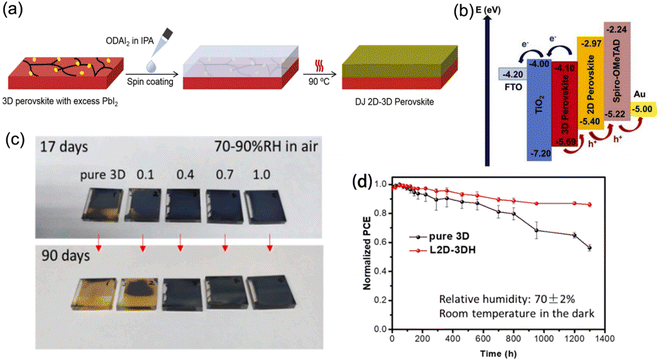 | ||
| Fig. 16 (a) Procedure for fabricating DJ 2D–3D perovskites. (b) Schematic diagram of the energy alignment for DJ 2D–3D PSCs. Reproduced with permission from ref. 132. Copyright 2020 Elsevier. (c) Optical images of pure 3D and 2D–3D perovskite films stored under a 70–90% RH humidity atmosphere for 90 days. (d) PCE decay curves of the pure 3D and L2D–3DH devices. Reproduced with permission from ref. 135. Copyright 2021 Elsevier. | ||
By depositing a 2D perovskite capping layer on 3D perovskite films, the 2D–3D perovskite hybrid structure provides a prospective strategy to balance the efficiency and stability of PSCs. Moreover, inspired by the previous research on 2D perovskites, the organic spacers in DJ phase perovskites can be rationally tailored to further enhance the efficiency and stability of devices.
5. Conclusions and outlooks
In conclusion, the remarkable advances in quasi-2D DJ perovskites for photovoltaics have been systematically reviewed. The basic properties of quasi-2D DJ perovskites, such as superior stability, high Eb, and compositional flexibility and tunable properties, were discussed in detail. Moreover, owing to the valuable investigation of strategies involving compositional engineering, solvent engineering, additive addition, and an annealing process for improving film quality, quasi-2D DJ perovskites have been demonstrated to be promising absorption materials in realizing both long-term stability and high photovoltaic performance for PSCs. Surface/interface modification and a 2D–3D hybrid perovskite heterojunction are also considered to be potential strategies in optimizing the fabrication of DJ PSCs. However, some key challenges persist, and knowledge gaps still need to be filled to provide an in-depth understanding of quasi-2D DJ perovskites, as follows.5.1 Uniform QW distribution
Quasi-2D DJ perovskites processed using a solution method always exhibit mixed phase and random QW distribution, which are ascribed to the intermediate phases incorporated by the solvent and the strong electrostatic affinity between spacer cations and inorganic slabs. The phase diversity in perovskites leads to a non-flat energy landscape, which suppresses the charge transport and separation and therefore deteriorates the device performance. Moreover, the random distribution of multiple QWs reduces the stability of devices. In contrast, a uniform QW distribution accompanied with a flattened energy landscape contributes to a larger carrier diffusion length and higher stability. Hence, it is crucial to further explore a method to effectively control and optimize the QW distribution of DJ perovskite films. For instance, additives that are able to reduce nucleation sites during the film formation ought to be utilized to form a regular QW distribution. An ionic liquid solvent such as MAAc is also considered to be effective in narrowing the n value distribution and affording pure-phase films.5.2 Design of organic spacer cations
Due to the fact that quantum/dielectric confinement both occur while the perovskite crystal dimension decreases, 2D perovskites exhibit suboptimal optoelectronic behavior compared to their 3D counterparts. Apart from dimensionality, the insulating organic spacer, from which the quantum confinement and dielectric confinement are derived, also plays an important role in film properties and device performance. Though DJ phase perovskites exhibit a smaller Eb than RP phase analogs, it is still vital to design appropriate organic spacers while simultaneously considering conductivity and hydrophobicity. Inspired by previous work, the organic spacer cations with an alkyl chain or aromatic unit, and fluorinated or sulfurated organic spacers, may offer an effective approach to achieve efficient and stable PSCs. Challenges also exist in generating DJ perovskite phases from bifunctional organic spacers, which can often lead to the formation of low-dimensional 1D structures. Thus, it is vital to consider the feasibility for the successful formation of typical DJ phase layered perovskites when tailoring organic cations.5.3 Crystallization kinetics
Generally, the spacer layers in small n value based quasi-2D perovskite films tend to grow preferentially parallel with respect to substrates, which is relevant to the lattice matching degree between the perovskite absorber and substrate, as well as the electrostatic interaction between charged groups in solution and the substrate surface. This would impede the charge transport from perovskites to the adjacent layer. Moreover, the orientation of the phase with a small n value at the bottom of film is different from that with a larger n value at the top of the film, which leads to the existence of a barrier for charge transport. Thus, further in-depth study into the crystallization kinetics of quasi-2D DJ perovskites is required.5.4 Degradation mechanisms
It is universally accepted that the structural stability of quasi-2D DJ perovskites is greater than their RP phase counterparts, which is attributed to the absence of van der Waals gaps. The increase in the n value in DJ phase perovskites contributes to an improvement in charge transport along the vertical orientation that promotes the photovoltaic properties, while resulting in the inferior stability due to the reduced hydrophobicity. Owing to depressed moisture resistance, quasi-2D DJ perovskites with a high n value more easily experience PCE degradation while stored in air. Moreover, the migration of Pb2+ and I− from the perovskite absorber to adjacent layers and/or electrode also degrades the optoelectric properties of quasi-2D DJ PSCs. Therefore, thorough investigation of the degradation mechanism of DJ perovskites with a high n value and their devices ought to be implemented.Finally, it is believed that more quasi-2D DJ phase perovskites will be prepared and more fresh research output will be published to accelerate the practical applications of photovoltaic technology.
Conflicts of interest
The authors declare no conflicts of interest.Acknowledgements
This work was financially supported by the National Key Research and Development Program of China (2022YFB3805203), the National Natural Science Foundation of China (No. 52273245), the Strategic Priority Research Program of Chinese Academy of Sciences (No. XDB36000000), the Natural Science Foundation of Anhui Province (2008085ME132), the Outstanding Youth Fund of Anhui Provincial Department of Education (2022AH020064), the Anhui Provincial Natural Science Foundation (2308085QE138), the Natural Science Foundation of Anhui Provincial Education Department (2023AH050915), and the Scientific Research starting Foundation of Anhui Polytechnic University of China (2022YQQ040, 2022YQQ042).References
- A. Kojima, K. Teshima, Y. Shirai and T. Miyasaka, J. Am. Chem. Soc., 2009, 131, 6050–6051 CrossRef CAS PubMed.
- S. D. Wolf, J. Holovsky, S. J. Moon, P. Löper, B. Niesen, M. Ledinsky, F. J. Haug, J. H. Yum and C. Ballif, J. Phys. Chem. Lett., 2014, 5, 1035–1039 CrossRef PubMed.
- G. E. Eperon, S. D. Stranks, C. Menelaou, M. B. Johnston, L. M. Herza and H. J. Snaith, Energy Environ. Sci., 2014, 7, 982–988 RSC.
- D. Shi, V. Adinolfi, R. Comin, M. Yuan, E. Alarousu, A. Buin, Y. Chen, S. Hoogland and A. Rothenberger, et al. , Science, 2015, 347, 519–522 CrossRef CAS PubMed.
- Y. Rong, Y. Hu, A. Mei, H. Tan, M. I. Saidaminov, S. I. Seok, M. D. Mcgehee, E. H. Sargent and H. Han, Science, 2018, 361, eaat8235 CrossRef PubMed.
- J. Park, J. Kim, H. S. Yun, M. J. Paik, E. Noh, H. J. Mun, M. G. Kim, T. J. Shin and S. I. Seok, Nature, 2023, 616, 724–730 CrossRef CAS PubMed.
- NREL, Best Research-Cell Efficiency Chart, https://www.nrel.gov/pv/cell-efficiency.html.
- Q. Jiang, J. Tong, Y. Xian, R. A. Kerner, S. P. Dunfield, C. Xiao, R. A. Scheidt, D. Kuciauskas, X. Wang, M. P. Hautzinger, R. Tirawat, M. C. Beard, D. P. Fenning, J. J. Berry, B. W. Larson, Y. Yan and K. Zhu, Nature, 2022, 611, 278–283 CrossRef CAS PubMed.
- H. Min, D. Y. Lee, J. Kim, G. Kim, K. S. Lee, J. Kim, M. J. Paik, Y. K. Kim, K. S. Kim, M. G. Kim, T. J. Shin and S. I. Seok, Nature, 2021, 598, 444–450 CrossRef CAS PubMed.
- J. Jeong, M. Kim, J. Seo, H. Lu, P. Ahlawat, A. Mishra, Y. Yang, M. A. Hope, F. T. Eickemeyer, M. Kim, Y. J. Yoon, I. W. Choi, B. P. Darwich, S. J. Choi, Y. Jo, J. H. Lee, B. Walker, S. M. Zakeeruddin, L. Emsley, U. Rothlisberger, A. Hagfeldt, D. S. Kim, M. Grätzel and J. Y. Kim, Nature, 2021, 592, 381–385 CrossRef CAS PubMed.
- P. Huang, S. Kazim, M. Wang and S. Ahmad, ACS Energy Lett., 2019, 4, 2960–2974 CrossRef CAS.
- Y. Han, S. Meyer, Y. Dkhissi, K. Weber, J. M. Pringle, U. Bach, L. Spiccia and Y. B. Cheng, J. Mater. Chem. A, 2015, 3, 8139–8147 RSC.
- T. A. Berhe, W. N. Su, C. H. Chen, C. J. Pan, J. H. Cheng, H. M. Chen, M. C. Tsai, L. Y. Chen, A. A. Dubale and B. J. Hwang, Energy Environ. Sci., 2016, 9, 323–356 RSC.
- B. Conings, J. Drijkoningen, N. Gauquelin, A. Babayigit, J. D'Haen, L. D'Olieslaeger, A. Ethirajan, J. Verbeeck, J. Manca, E. Mosconi, F. D. Angelis and H. G. Boyen, Adv. Energy Mater., 2015, 5, 1500477 CrossRef.
- S. Akin, E. Akman and S. Sonmezoglu, Adv. Funct. Mater., 2020, 30, 2002964 CrossRef CAS.
- T. Du, T. J. Macdonald, R. X. Yang, M. Li, Z. Jiang, L. Mohan, W. Xu, Z. Su, X. Gao, R. Whiteley, C. T. Lin, G. Min, S. A. Haque, J. R. Durrant, K. A. Persson, M. A. McLachlan and J. Briscoe, Adv. Mater., 2022, 34, 2107850 CrossRef CAS PubMed.
- J. Zhang, G. Hodes, Z. Jin and S. Liu, Angew. Chem., Int. Ed., 2019, 58, 15596–15618 CrossRef CAS PubMed.
- Y. Wang, Y. Chen, T. Zhang, X. Wang and Y. Zhao, Adv. Mater., 2020, 32, 2001025 CrossRef CAS PubMed.
- F. Lin, Y. Yang, C. Zhu, T. Chen, S. Ma, Y. Luo, L. Zhu and X. Guo, Acta Phys.-Chim. Sin., 2022, 38, 2005007 Search PubMed.
- W. Ke, L. Mao, C. C. Stoumpos, J. Hoffman, I. Spanopoulos, A. D. Mohite and M. G. Kanatzidis, Adv. Energy Mater., 2019, 9, 1803384 CrossRef.
- N. Zhou, Y. Shen, L. Li, S. Tan, N. Liu, G. Zheng, Q. Chen and H. Zhou, J. Am. Chem. Soc., 2018, 140, 459–465 CrossRef CAS PubMed.
- J. Liang, Z. Zhang, Q. Xue, Y. Zheng, X. Wu, Y. Huang, X. Wang, C. Qin, Z. Chen and C. C. Chen, Energy Environ. Sci., 2022, 15, 296–310 RSC.
- Q. Cao, P. Li, W. Chen, S. Zang, L. Han, Y. Zhang and Y. Song, Nano Today, 2022, 43, 101394 CrossRef CAS.
- Z. Zhai, J. Chen, Q. Liu, S. Jiang and Y. Li, ACS Appl. Mater. Interfaces, 2023, 15, 38068–38079 CrossRef CAS PubMed.
- B. Saparov and D. B. Mitzi, Chem. Rev., 2016, 116, 4558–4596 CrossRef CAS PubMed.
- G. Wu, R. Liang, Z. Zhang, M. Ge, G. Xing and G. Sun, Small, 2021, 17, 2103514 CrossRef CAS PubMed.
- L. Mao, C. C. Stoumpos and M. G. Kanatzidis, J. Am. Chem. Soc., 2018, 141, 1171–1190 CrossRef PubMed.
- H. Lai, D. Lu, Z. Xu, N. Zheng, Z. Xie and Y. Liu, Adv. Mater., 2020, 32, 2001470 CrossRef CAS PubMed.
- H. Ren, S. Yu, L. Chao, Y. Xia, Y. Sun, S. Zuo, F. Li, T. Niu, Y. Yang, H. Ju, B. Li, H. Du, X. Gao, J. Zhang, J. Wang, L. Zhang, Y. Chen and W. Huang, Nat. Photonics, 2020, 14, 154–163 CrossRef CAS.
- Z. Xu, D. Lu, F. Liu, H. Lai, X. Wan, X. Zhang, Y. Liu and Y. Chen, ACS Nano, 2020, 14, 4871–4881 CrossRef CAS PubMed.
- G. Wu, T. Yang, X. Li, N. Ahmad, X. Zhang, S. Yue, J. Zhou, Y. Li, H. Wang, X. Shi, S. Liu, K. Zhao, H. Zhou and Y. Zhang, Matter, 2021, 4, 582–599 CrossRef CAS.
- Z. Xu, D. Lu, X. Dong, M. Chen, Q. Fu and Y. Liu, Adv. Mater., 2021, 33, 2105083 CrossRef CAS PubMed.
- L. Mao, W. Ke, L. Pedesseau, Y. Wu, C. Katan, J. Even, M. R. Wasielewski, C. C. Stoumpos and M. G. Kanatzidis, J. Am. Chem. Soc., 2018, 140, 3775–3783 CrossRef CAS PubMed.
- C. Ma, D. Shen, T. W. Ng, M. F. Lo and C. S. Lee, Adv. Mater., 2018, 30, 1800710 CrossRef PubMed.
- S. Ahmad, P. Fu, S. Yu, Q. Yang, X. Liu, X. Wang, X. Wang and C. Li, Joule, 2019, 3, 794–806 CrossRef CAS.
- C. M. M. Soe, C. C. Stoumpos, M. Kepenekian, B. Traoré, H. Tsai, W. Nie, B. Wang, C. Katan, R. Seshadri, A. D. Mohite, J. Even, T. J. Marks and M. G. Kanatzidis, J. Am. Chem. Soc., 2017, 139, 16297–16309 CrossRef CAS PubMed.
- Y. Zhang, J. Chen, X. Lian, M. Qin, J. Li, T. R. Andersen, X. Lu, G. Wu, H. Li and H. Chen, Small Methods, 2019, 3, 1900375 CrossRef CAS.
- H. Gu, C. Liang, Y. Xia, Q. Wei, T. Liu, Y. Yang, W. Hui, H. Chen, T. Niu, L. Chao, Z. Wu, X. Xie, J. Qiu, G. Shao, X. Gao, G. Xing, Y. Chen and W. Huang, Nano Energy, 2019, 65, 104050 CrossRef CAS.
- A. Ducinskas, G. Y. Kim, D. Moia, A. Senocrate, Y. Wang, M. A. Hope, A. Mishra, D. J. Kubicki, M. Siczek, W. Bury, T. Schneeberger, L. Emsley, J. V. Milić, J. Maier and M. Grätzel, ACS Energy Lett., 2020, 6, 337–344 CrossRef.
- L. Pedesseau, D. Sapori, B. Traore, R. Robles, H. H. Fang, M. A. Loi, H. Tsai, W. Nie, J. C. Blancon, A. Neukirch, S. Tretiak, A. D. Mohite, C. Katan, J. Even and M. Kepenekian, ACS Nano, 2016, 10, 9776–9786 CrossRef CAS PubMed.
- R. Chakraborty and A. Nag, Phys. Chem. Chem. Phys., 2021, 23, 82–93 RSC.
- C. M. Mauck and W. A. Tisdale, Trends Chem., 2019, 1, 380–393 CrossRef CAS.
- D. T. Gangadharan and D. Ma, Energy Environ. Sci., 2019, 12, 2860–2889 RSC.
- E. I. Marchenko, V. V. Korolev, A. Mitrofanov, S. A. Fateev, E. A. Goodilin and A. B. Tarasov, Chem. Mater., 2021, 33, 1213–1217 CrossRef CAS.
- L. N. Quan, M. Yuan, R. Comin, O. Voznyy, E. M. Beauregard, S. Hoogland, A. Buin, A. R. Kirmani, K. Zhao, A. Amassian, D. H. Kim and E. H. Sargent, J. Am. Chem. Soc., 2016, 138, 2649–2655 CrossRef CAS PubMed.
- W. Li, X. Feng, K. Guo, W. Pan, M. Li, L. Liu, J. Song, Y. He and H. Wei, Adv. Mater., 2023, 35, 2211808 CrossRef CAS PubMed.
- K. Domanski, B. Roose, T. Matsui, M. Saliba, S. H. Turren-Cruz, J. P. Correa-Baena, C. R. Carmona, G. Richardson, J. M. Foster, F. D. Angelis, J. M. Ball, A. Petrozza, N. Mine, M. K. Nazeeruddin, W. Tress, M. Grätzel, U. Steiner, A. Hagfeldt and A. Abate, Energy Environ. Sci., 2017, 10, 604–613 RSC.
- J. Li, Q. Dong, N. Li and L. Wang, Adv. Energy Mater., 2017, 7, 1602922 CrossRef.
- M. Bag, L. A. Renna, R. Y. Adhikari, S. Karak, F. Liu, P. M. Lahti, T. P. Russell, M. T. Tuominen and D. Venkataraman, J. Am. Chem. Soc., 2015, 137, 13130–13137 CrossRef CAS PubMed.
- P. Liu, W. Wang, S. Liu, H. Yang and Z. Shao, Adv. Energy Mater., 2019, 9, 1803017 CrossRef.
- Y. Lin, Y. Bai, Y. Fang, Q. Wang, Y. Deng and J. Huang, ACS Energy Lett., 2017, 2, 1571–1572 CrossRef CAS.
- Y. Lin, Y. Bai, Y. Fang, Z. Chen, S. Yang, X. Zheng, S. Tang, Y. Liu, J. Zhao and J. Huang, J. Phys. Chem. Lett., 2018, 9, 654–658 CrossRef CAS PubMed.
- X. Jiang, J. Zhang, S. Ahmad, D. Tu, X. Liu, G. Jia, X. Guo and C. Li, Nano Energy, 2020, 75, 104892 CrossRef CAS.
- Y. Zhang, Y. Liu, Z. Xu, Z. Yang and S. Liu, Small, 2020, 16, 2003145 CrossRef CAS PubMed.
- P. Li, Y. Zhang, C. Liang, G. Xing, X. Liu, F. Li, X. Liu, X. Hu, G. Shao and Y. Song, Adv. Mater., 2018, 30, 1805323 CrossRef PubMed.
- J. Chen, B. Wang, G. Huang, Q. Cheng, Y. Li, X. Li, S. Li, K. Li, L. Zhu, Z. Zhai, Y. Zhang and H. Zhou, Sol. RRL, 2022, 6, 2200636 CrossRef CAS.
- G. Huang, J. Chen, B. Wang, Q. Cheng, Y. Li, S. U. Zafar, T. Yue, Y. Yang, W. Du, H. Zhang, X. Liu, Y. Zhang and H. Zhou, Nano Lett., 2022, 22, 7545–7553 CrossRef CAS PubMed.
- Y. Li, J. V. Milić, A. Ummadisingu, J. Y. Seo, J. H. Im, H. S. Kim, Y. Liu, M. I. Dar, S. M. Zakeeruddin, P. Wang, A. Hagfeldt and M. Grätzel, Nano Lett., 2018, 19, 150–157 CrossRef PubMed.
- C. Katan, N. Mercier and J. Even, Chem. Rev., 2019, 119, 3140–3192 CrossRef CAS PubMed.
- K. Tanaka, T. Takahashi, T. Kondo, T. Umebayashi, K. Asai and K. Ema, Phys. Rev. B: Condens. Matter Mater. Phys., 2005, 71, 045312 CrossRef.
- X. F. He, Phys. Rev. B: Condens. Matter Mater. Phys., 1991, 43, 2063 CrossRef PubMed.
- H. Mathieu, P. Lefebvre and P. Christol, Phys. Rev. B: Condens. Matter Mater. Phys., 1992, 46, 4092 CrossRef PubMed.
- J. C. Blancon, A. V. Stier, H. Tsai, W. Nie, C. C. Stoumpos, B. Traoré, L. Pedesseau, M. Kepenekian, F. Katsutani, G. T. Noe, J. Kono, S. Tretiak, S. A. Crooker, C. Katan, M. G. Kanatzidis, J. J. Crochet, J. Even and A. D. Mohite, Nat. Commun., 2018, 9, 2254 CrossRef PubMed.
- V. M. Agranovich, Y. N. Gartstein and M. Litinskaya, Chem. Rev., 2011, 111, 5179–5214 CrossRef CAS PubMed.
- B. R. Sutherland and E. H. Sargent, Nat. Photonics, 2016, 10, 295–302 CrossRef CAS.
- F. O. Saouma, C. C. Stoumpos, J. Wong, M. G. Kanatzidis and J. I. Jang, Nat. Commun., 2017, 8, 742 CrossRef CAS PubMed.
- N. Wang, L. Cheng, R. Ge, S. Zhang, Y. Miao, W. Zou, C. Yi, Y. Sun, Y. Cao, R. Yang, Y. Wei, Q. Guo, Y. Ke, M. Yu, Y. Jin, Y. Liu, Q. Ding, D. Di, L. Yang, G. Xing, H. Tian, C. Jin, F. Gao, R. H. Friend, J. Wang and W. Huang, Nat. Photonics, 2016, 10, 699–704 CrossRef CAS.
- M. Yuan, L. N. Quan, R. Comin, G. Walters, R. Sabatini, O. Voznyy, S. Hoogland, Y. Zhao, E. M. Beauregard, P. Kanjanaboos, Z. Lu, D. H. Kim and E. H. Sargent, Nat. Nanotechnol., 2016, 11, 872–877 CrossRef CAS PubMed.
- L. Li, Z. Sun, P. Wang, W. Hu, S. Wang, C. Ji, M. Hong and J. Luo, Angew. Chem., 2017, 129, 12318–12322 CrossRef.
- S. Han, P. Wang, J. Zhang, X. Liu, Z. Sun, X. Huang, L. Li, C. Ji, W. Zhang, B. Teng, W. Hu, M. Hong and J. Luo, Laser Photonics Rev., 2018, 12, 1800060 CrossRef.
- H. Wang, C. C. S. Chan, M. Chu, J. Xie, S. Zhao, X. Guo, Q. Miao, K. S. Wong, K. Yan and J. Xu, Sol. RRL, 2020, 4, 1900578 CrossRef CAS.
- S. Sourisseau, N. Louvain, W. Bi, N. Mercier, D. Rondeau, F. Boucher, J. Y. Buzaré and C. Legein, Chem. Mater., 2007, 19, 600–607 CrossRef CAS.
- Y. Zheng, T. Niu, J. Qiu, L. Chao, B. Li, Y. Yang, Q. Li, C. Lin, X. Gao, C. Zhang, Y. Xia, Y. Chen and W. Huang, Sol. RRL, 2019, 3, 1900090 CrossRef.
- X. Li, W. Ke, B. Traoré, P. Guo, I. Hadar, M. Kepenekian, J. Even, C. Katan, C. C. Stoumpos, R. D. Schaller and M. G. Kanatzidis, J. Am. Chem. Soc., 2019, 141, 12880–12890 CrossRef CAS PubMed.
- B. E. Cohen, Y. Li, Q. Meng and L. Etgar, Nano Lett., 2019, 19, 2588–2597 CrossRef CAS PubMed.
- S. Yu, Y. Yan, M. Abdellah, T. Pullerits, K. Zheng and Z. Liang, Small, 2019, 15, 1905081 CrossRef CAS PubMed.
- X. Zhao, T. Liu, A. B. Kaplan, C. Yao and Y. L. Loo, Nano Lett., 2020, 20, 8880–8889 CrossRef CAS PubMed.
- S. Ahmad, R. Lu, Y. Liu, X. Liu, Q. Yang, X. Guo and C. Li, Nano Energy, 2022, 103, 107822 CrossRef CAS.
- W. Ke, C. Chen, I. Spanopoulos, L. Mao, I. Hadar, X. Li, J. M. Hoffman, Z. Song, Y. Yan and M. G. Kanatzidis, J. Am. Chem. Soc., 2020, 142, 15049–15057 CrossRef CAS PubMed.
- Y. Guo, M. Sun, W. Yang, S. Yuan, H. Xiong, Z. Tan, J. Fan and W. Li, J. Phys. Chem. C, 2022, 126, 9425–9436 CrossRef CAS.
- Z. Lu, C. Li, H. Lai, X. Zhou, C. Wang, X. Liu, F. Guo and C. Pan, Nano Res., 2022, 16, 1–7 Search PubMed.
- L. Gao, X. Li, B. Traore, Y. Zhang, J. Fang, Y. Han, J. Even, C. Katan, K. Zhao, S. Liu and M. G. Kanatzidis, J. Am. Chem. Soc., 2021, 143, 12063–12073 CrossRef CAS PubMed.
- J. C. Blancon, H. Tsai, W. Nie, C. C. Stoumpos, L. Pedesseau, C. Katan, M. Kepenekian, C. M. M. Soe, K. Appavoo, M. Y. Sfeir, S. Tretiak, P. M. Ajayan, M. G. Kanatzidis, J. Even, J. J. Crochet and A. D. Mohite, Science, 2017, 355, 1288–1292 CrossRef CAS PubMed.
- J. Xiang, X. Li, S. Gong, S. Wang, X. Chen and F. Zhang, Chem. Eng. J., 2023, 460, 141758 CrossRef CAS.
- X. Guo, Y. Gao, F. Long, L. Lin, Y. Wang, K. H. Ngai, Q. Wei, G. Xing, T. Shi, W. Xie, M. Long and J. Xu, Sol. RRL, 2023, 7, 2201021 CrossRef CAS.
- L. Zhang, G. Qi, Y. Zhang, H. Wu, X. Xu, G. Zhou, H. Zhu, X. Li, G. Wu and H. Chen, Chem. Eng. J., 2023, 451, 138654 CrossRef CAS.
- E. S. Vasileiadou, B. Wang, I. Spanopoulos, I. Hadar, A. Navrotsky and M. G. Kanatzidis, J. Am. Chem. Soc., 2021, 143, 2523–2536 CrossRef CAS PubMed.
- G. Lv, L. Li, D. Lu, Z. Xu, Y. Dong, Q. Li, Z. Chang, W. J. Yin and Y. Liu, Nano Lett., 2021, 21, 5788–5797 CrossRef CAS PubMed.
- B. Giese, M. Graber and M. Cordes, Curr. Opin. Chem. Biol., 2008, 12, 755–759 CrossRef CAS PubMed.
- D. Wang, S. C. Chen and Q. Zheng, J. Mater. Chem. A, 2021, 9, 11778–11786 RSC.
- A. Dučinskas, G. C. Fish, M. A. Hope, L. Merten, D. Moia, A. Hinderhofer, L. C. Carbone, J. E. Moser, F. Schreiber, J. Maier, J. V. Milić and M. Grätzel, J. Phys. Chem. Lett., 2021, 12, 10325–10332 CrossRef PubMed.
- M. Almalki, A. Dučinskas, L. C. Carbone, L. Pfeifer, L. Piveteau, W. Luo, E. Lim, P. A. Gaina, P. A. Schouwink, S. M. Zakeeruddin, J. V. Milić and M. Grätzel, Nanoscale, 2022, 14, 6771–6776 RSC.
- Y. Dong, X. Dong, D. Lu, M. Chen, N. Zheng, R. Wang, Q. Li, Z. Xie and Y. Liu, Adv. Mater., 2023, 35, 2205258 CrossRef CAS PubMed.
- Y. Liu, H. Zhou, Y. Ni, J. Guo, R. Lu, C. Li and X. Guo, Joule, 2023, 7, 1016–1032 CrossRef CAS.
- C. Lermer, A. Senocrate, I. Moudrakovski, T. Seewald, A. Hatz, P. Mayer, F. Pielnhofer, J. A. Jaser, L. Schmidt-Mende, J. Maier and B. V. Lotsch, Chem. Mater., 2018, 30, 6289–6297 CrossRef CAS.
- J. Wang, D. Lin, Y. Chen, S. Luo, L. Ke, X. Ren, S. Cui, L. Zhang, Z. Li, K. Meng, Y. Lin, L. Ding and Y. Yuan, Sol. RRL, 2020, 4, 2000371 CrossRef CAS.
- L. Cheng, Z. Liu, S. Li, Y. Zhai, X. Wang, Z. Qiao, Q. Xu, K. Meng, Z. Zhu and G. Chen, Angew. Chem., 2021, 133, 869–877 CrossRef.
- M. Safdari, P. H. Svensson, M. T. Hoang, I. Oh, L. Kloo and J. M. Gardner, J. Mater. Chem. A, 2016, 4, 15638–15646 RSC.
- M. Safdari, D. Phuyal, B. Philippe, P. H. Svensson, S. M. Butorin, K. O. Kvashnina, H. Rensmo, L. Kloo and J. M. Gardner, J. Mater. Chem. A, 2017, 5, 11730–11738 RSC.
- T. Niu, H. Ren, B. Wu, Y. Xia, X. Xie, Y. Yang, X. Gao, Y. Chen and W. Huang, J. Phys. Chem. Lett., 2019, 10, 2349–2356 CrossRef CAS PubMed.
- P. Li, X. Liu, Y. Zhang, C. Liang, G. Chen, F. Li, M. Su, G. Xing, X. Tao and Y. Song, Angew. Chem., Int. Ed., 2020, 59, 6909–6914 CrossRef CAS PubMed.
- F. Li, J. Zhang, S. B. Jo, M. Qin, Z. Li, T. Liu, X. Lu, Z. Zhu and A. K. Y. Jen, Small Methods, 2020, 4, 1900831 CrossRef CAS.
- P. Su, L. Bai, H. Bi, B. Liu, S. Chen, D. Lee, H. Yang, C. Chen, Z. Zang and J. Chen, J. Power Sources, 2021, 506, 230213 CrossRef CAS.
- H. Yu, Y. Xie, J. Zhang, J. Duan, X. Chen, Y. Liang, K. Wang and L. Xu, Adv. Sci., 2021, 8, 2004510 CrossRef CAS PubMed.
- L. Jin, N. Ren, P. Wang, R. Li, Q. Xue, F. Huang, X. Zhang, Y. Zhao and X. Zhang, Small, 2023, 19, 2205088 CrossRef CAS PubMed.
- X. Zhang, T. Yang, X. Ren, L. Zhang, K. Zhao and S. Liu, Adv. Energy Mater., 2021, 11, 2002733 CrossRef CAS.
- G. Lv, L. Li, D. Lu, Z. Xu, Y. Dong, Q. Li, Z. Chang, W. J. Yin and Y. Liu, Nano Lett., 2021, 21, 5788–5797 CrossRef CAS PubMed.
- H. Wu, X. Lian, J. Li, Y. Zhang, G. Zhou, X. Wen, Z. Xie, H. Zhu, G. Wu and H. Chen, J. Mater. Chem. A, 2021, 9, 12566–12573 RSC.
- H. Wu, X. Lian, S. Tian, Y. Zhang, M. Qin, Y. Zhang, F. Wang, X. Lu, G. Wu and H. Chen, Sol. RRL, 2020, 4, 2000087 CrossRef CAS.
- M. Chen, M. G. Ju, M. Hu, Z. Dai, Y. Hu, Y. Rong, H. Han, X. C. Zeng, Y. Zhou and N. P. Padture, ACS Energy Lett., 2018, 4, 276–277 CrossRef.
- W. Li, S. Sidhik and B. Traore, et al. , Nat. Nanotechnol., 2022, 17, 45–52 CrossRef CAS PubMed.
- H. Wang, Z. Qin, J. Xie, S. Zhao, K. Liu, X. Guo, G. Li, X. Lu, K. Yan and J. Xu, Small, 2020, 16, 2003098 CrossRef CAS PubMed.
- D. Lu, G. Lv, Z. Xu, Y. Dong, X. Ji and Y. Liu, J. Am. Chem. Soc., 2020, 142, 11114–11122 CrossRef CAS PubMed.
- M. C. Gélvez-Rueda, P. Ahlawat, L. Merten, F. Jahanbakhshi, M. Mladenović, A. Hinderhofer, M. I. Dar, Y. Li, A. Dučinskas, B. Carlsen, W. Tress, A. Ummadisingu, S. M. Zakeeruddin, F. Schreiber, A. Hagfeldt, U. Rothlisberger, F. C. Grozema, J. V. Milić and M. Graetzel, Adv. Funct. Mater., 2020, 30, 2003428 CrossRef.
- T. Zhang, M. I. Dar, G. Li, F. Xu, N. Guo, M. Grätzel and Y. Zhao, Sci. Adv., 2017, 3, e1700841 CrossRef PubMed.
- Y. Lei, Z. Li, H. Wang, Q. Wang, G. Peng, Y. Xu, H. Zhang, G. Wang, L. Ding and Z. Jin, Sci. Bull., 2022, 67, 1352–1361 CrossRef CAS PubMed.
- W. Ning and F. Gao, Adv. Mater., 2019, 31, 1900326 CrossRef PubMed.
- F. Gu, S. Ye, Z. Zhao, H. Rao, Z. Liu, Z. Bian and C. Huang, Sol. RRL, 2018, 2, 1800136 CrossRef.
- L. Mao, P. Guo, M. Kepenekian, I. Spanopoulos, Y. He, C. Katan, J. Even, R. D. Schaller, R. Seshadri, C. C. Stoumpos and M. G. Kanatzidis, J. Am. Chem. Soc., 2020, 142, 8342–8351 CrossRef CAS PubMed.
- W. Zha, L. Zhang, L. Wen, J. Kang, Q. Luo, Q. Chen, S. Yang and C. Ma, Acta Phys.-Chim. Sin., 2022, 38, 2003022 Search PubMed.
- J. Zhang, L. Zhang, X. Li, X. Zhu, J. Yu and K. Fan, ACS Sustainable Chem. Eng., 2019, 7, 3487–3495 CrossRef CAS.
- P. Cheng, Z. Xu, J. Li, Y. Liu, Y. Fan, L. Yu, D. M. Smilgies, C. Müller, K. Zhao and S. F. Liu, ACS Energy Lett., 2018, 3, 1975–1982 CrossRef CAS.
- J. Qiu, Y. Xia, Y. Zheng, W. Hui, H. Gu, W. Yuan, H. Yu, L. Chao, T. Niu, Y. Yang, X. Gao, Y. Chen and W. Huang, ACS Energy Lett., 2019, 4, 1513–1520 CrossRef CAS.
- C. M. M. Soe, W. Nie, C. C. Stoumpos, H. Tsai, J. C. Blancon, F. Liu, J. Even, T. J. Marks, A. D. Mohite and M. G. Kanatzidis, Adv. Energy Mater., 2018, 8, 1700979 CrossRef.
- Y. Chen, J. Hu, Z. Xu, Z. Jiang, S. Chen, B. Xu, X. Xiao, X. Liu, K. Forberich, C. J. Brabec, Y. Mai and F. Guo, Adv. Funct. Mater., 2022, 32, 2112146 CrossRef CAS.
- R. D. Chavan, P. Yadav and S. Satapathi, ACS Appl. Energy Mater., 2022, 5, 13723–13734 CrossRef.
- H. Zhang, M. Hou, Y. Xia, Q. Wei, Z. Wang, Y. Cheng, Y. Chen and W. Huang, J. Mater. Chem. A, 2018, 6, 9264–9270 RSC.
- M. Daub and H. Hillebrecht, Angew. Chem., 2015, 127, 11168–11169 CrossRef.
- J. Wang, S. Luo, Y. Lin, Y. Chen, Y. Deng, Z. Li, K. Meng, G. Chen, T. Huang, S. Xiao, H. Huang, C. Zhou, L. Ding, J. He, J. Huang and Y. Yuan, Nat. Commun., 2020, 11, 582 CrossRef CAS PubMed.
- G. Ren, C. Yan, L. Xiao, X. Wu, S. Peng, W. Lin, W. Tan, Y. Liu and Y. Min, ACS Appl. Energy Mater., 2022, 5, 9837–9845 CrossRef CAS.
- Y. C. Liu, J. T. Lin, Y. L. Lee, C. M. Hung, T. C. Chou, W. C. Chao, Z. X. Huang, T. H. Chiang, C. W. Chiu, W. T. Chuang and P. T. Chou, J. Am. Chem. Soc., 2022, 144, 14897–14906 CrossRef CAS PubMed.
- X. Jiang, J. Zhang, S. Ahmad, D. Tu, X. Liu, G. Jia, X. Guo and C. Li, Nano Energy, 2020, 75, 104892 CrossRef CAS.
- X. Wang, Y. Zhao, B. Li, X. Han, Z. Jin, Y. Wang, Q. Zhang and Y. Rui, ACS Appl. Mater. Interfaces, 2021, 14, 22879–22888 CrossRef PubMed.
- Y. Yu, R. Liu, M. Xu and H. Yu, EcoMat, 2023, 5, e12272 CrossRef CAS.
- W. Li, X. Gu, C. Shan, X. Lai, X. W. Sun and A. K. K. Kyaw, Nano Energy, 2022, 91, 106666 CrossRef CAS.
| This journal is © The Royal Society of Chemistry 2023 |


