Recent progress in morphology optimization in perovskite solar cell
Naveen Kumar
Tailor
 a,
Mojtaba
Abdi-Jalebi
 b,
Vinay
Gupta
c,
Hanlin
Hu
d,
M. Ibrahim
Dar
e,
Gang
Li
 d and
Soumitra
Satapathi
 *a
*a
aDepartment of Physics, Indian Institute of Technology Roorkee, Roorkee, Uttarakhand 247667, India. E-mail: ssphf.fph@iitr.ac.in
bInstitute for Materials Discovery, University College London, Torrington Place, London, WC1E 7JE, UK
cDepartment of Mechanical Engineering, Khalifa University of Science and Technology, Masdar campus, Abu Dhabi 54224, United Arab Emirates
dElectronic and Information Engineering, The Hong Kong Polytechnic University, 11 Yuk Choi Rd, Hung Hom, Hong Kong. E-mail: gang.w.li@polyu.edu.hk
eCavendish Laboratory, University of Cambridge, J J Thomson Avenue, Cambridge, CB3 0HE, UK
First published on 30th April 2020
Abstract
Hybrid organic–inorganic halide perovskite based solar cell technology has passed through a phase of unprecedented growth in the efficiency scale from 3.8% to above 25% within a decade. This technology has drawn tremendous research interest because of facile solution processability, ease of large scale manufacturing and ultra-low cost production of perovskite based thin film solar cells. It has been observed that performances of perovskite-based solar cells are extremely dependent on the morphology and crystallinity of the perovskite layer. The high-quality perovskite films have made a significant impact on the fabrication of efficient and stable hybrid perovskite solar cells. It has also been observed that device lifetime depends on the perovskite morphology; devices with larger perovskite grains degrade slowly than those of the smaller ones. Various methods of perovskite growth such as sequential deposition, doctor blading, slot die coating and spray coating have been applied to achieve the most appropriate morphology necessary for highly efficient and stable solar cells. This review focuses on the recent progress in morphology optimizations by various processing condition such as annealing condition, additive effects, Lewis acid–base adduct approach, precursor solution aging and post-device ligand treatment emphasizing on grain sizes, film uniformity, defect passivation, ambient compatibility and device efficiency and stability. In this review, we also discussed recently developed bifacial stamping technique and deposition methods for large-area and roll-to-roll fabrication of highly efficient and stable perovskite solar cells.
Naveen Kumar Tailor is currently a PhD student at the Department of Physics, Indian Institute of Technology Roorkee, India. His research interest is photophysics study and optoelectronic applications of perovskite single crystals. |
Mojtaba Abdi-Jalebi is currently a lecturer at the Institute for Materials Discovery, University College London, and former research fellow at the Department of Physics, University of Cambridge, UK. His research investigates emerging semiconductors for electronics applications including solar-photovoltaics and lighting. He completed his PhD in 2018 at the Optoelectronics group, Cavendish Laboratory, University of Cambridge. Prior to this, Mojtaba obtained his MSc in Materials Science and Engineering from École Polytechnique Fédérale de Lausanne (EPFL) in Switzerland where he worked with Professor Michael Grätzel on development and implementation of novel materials in emerging solar cells. |
Vinay Gupta is an Indian materials scientist and a former senior scientist at the Physics of Energy Harvesting department of the National Physical Laboratory of India. Known for his studies on organic solar cells, carbon nanotubes arrays and Förster resonance energy transfer, Gupta is a former Alexander von Humboldt Fellow. The Council of Scientific and Industrial Research, the apex agency of the Government of India for scientific research, awarded him the Shanti Swarup Bhatnagar Prize for Science and Technology, one of the highest Indian science awards, for his contributions to physical sciences in 2017. |
Hanlin Hu received his PhD degree from the Department of Materials Science and Engineering at the King Abdullah University of Science and Technology (KAUST), Jeddah, Kingdom of Saudi Arabia, in October 2017. Then, he worked as a postdoctoral fellow in Prof. Gang Li's group in the Department of Electronic and Information Engineering, at the Hong Kong Polytechnic University, Hong Kong. He became an associate researcher in the college of materials science and engineering at Shenzhen University in March, 2019. His research interests include synchrotron based crystallography characterization, printing thin film solar cells and transistors. |
M. Ibrahim Dar is an Advanced Swiss National Science Foundation Fellow working in collaboration with Prof. Sir Richard Friend at the Cavendish Laboratory, the University of Cambridge. From 2014-2018, he worked as a Post-Doctoral Scientist with Prof. Michael Graetzel at EPFL Switzerland. He received his PhD in Nanoscience at Indian Institute of Science, Bangalore, India in 2014. His current research focuses on understanding structural, compositional and optoelectronic properties of materials for their application in light-harnessing and light-emitting devices. |
Dr Li Gang obtained his BS degree in Space Physics from Wuhan University (1994), followed by M.S. and PhD in Electrical Engineering and Condensed Matter Physics from Iowa State University, U.S.A. (2003), respectively. He has published ∼100 peer reviewed papers on Science, Nature Materials, Nature Photonics, Chem. Reviews, Nature Reviews Materials, JACS, Advanced Materials, Physical Reviews B etc. The papers have been cited ∼50,000 times according to Google Scholar. Dr Li is on the list of Thomson Reuter/ Clarivate Analytics Highly Cited Researchers in Materials Science (2014–2017) and Physics (2017), with a H-index of 63. |
Soumitra Satapathi is actively involved in Materials Science Research in IIT Roorkee where his main focus is next generation optoelectronics devices including high efficiency perovskite solar cells, photophysical studies in solar cells. Prof. Satapathi has graduated with PhD and MS in Physics from University of Massachusetts, USA. He has published more than 40 high impact journals papers and received numerous national and international awards. His research was featured in all leading national and international print and electronic media including Nature Asia, PTI, BBC, Quartz, USA Today, Times of India to name a few. |
1. Introduction
Since 2009, hybrid perovskites have turned into the star compounds/semiconductors within the field of solar cells, and hybrid perovskite solar cells (HPSCs) are perceived as the fourth era of solar cells.1–8 Perovskites are materials depicted by the formula ABX3, wherever X is an anion and A and B are cations of various sizes.9,10 The crystal structure and device architecture of perovskites is represented in Fig. 1.11,12 Their crystallographic stability and probable structure can be concluded by considering a tolerance factor t and an octahedral factor μ; here, t is characterized as the ratio of the distance A–X to the distance B–X in an idealized solid-sphere model , where rA, rB, and rX are the ionic radii of the corresponding ions and μ is defined as the ratio rB/rX.13,14 For halide perovskites (X = F, Cl, Br, I), generally 0.81 < t < 1.11 and 0.44 < μ < 0.90. If t lies in the narrower range 0.89 to 1.0, the cubic structure, with lower t values giving less symmetric tetragonal or orthorhombic structures.15,16 Compared with different types of solar cells, HPSCs have many points of interest. Firstly, the cost of HPSCs is very low in comparison to silicon-based solar cells. At the same level of efficiency, HPSCs is just 1/20 of the cost of silicon-based solar cells. Second, the highest efficiency of HPSCs is achieved up to 25.2%, which is near of silicon-based solar cells (∼26.1%) and efficiency of above 28% is forecasted for neat perovskite thin films with ideal transport layers.17 Third, the diffusion length of perovskite is greater than 1 micrometer, which is an order of magnitude larger than the absorption depth.1 Fourth, due to the development of roll-to-roll technology, HPSCs can be delivered at a large scale with a thickness of just a few micrometers. With the efforts of scientists throughout the world, the efficiency of HPSCs is right now exceeding the record for thin-film solar cells. In pursuing high efficiency of PSCs interface modification, compositional engineering and morphology tailoring haves been the major research focus.7,18–20 The perovskite film morphology and crystallinity are found to be crucial factors in fabricating highly efficient and stable solar cell.21 The objective of morphology control is to acquire compact, pinhole-free films with large grain sizes, high immaculateness, and better crystallinity, which is normally accomplished by tuning the annealing conditions to upgrade growth of the perovskite crystal, by incorporating additives in the precursor solution or by utilizing fast deposition–crystallization procedures.22–24
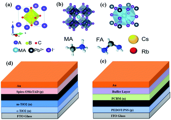 | ||
| Fig. 1 (a) Unit cell of a general cubic perovskite. (b) MAPbI3 illustrating the octahedral coordination around the lead ions. (c) MAPbI3 illustrating the cuboctahedra coordination around the organic ion. Reproduced by permission ref. 11, Copyright 2017 Royal Society of Chemistry. (d) n–i–p and (e) p–i–n perovskite solar cell device architectures. | ||
From these diverse investigations, it is obvious that optimizing the crystallization and grain growth condition is critical in accomplishing high-quality films to increase device performance. Since the morphology of the perovskite absorber thin film is one of the most critical factors that influence the overall power conversion efficiency of perovskite solar cells.12,25,26 A phenomenal amount of effort has been dedicated toward controlling perovskite crystallization for improved film uniformity and gaining a superior comprehension of these processes.5,21,25–28 Understanding the role of fabrication methodology in perovskite absorbers is important to increasing PV performance further and reducing the overall production costs for roll-to-roll production.29,30 Low-cost, easy reproduction, and facile deposition methods are favoured for the fabrication of perovskite thin films.31–34 Different strategies have already been subject to intense investigation, and have been checked for the fabrication of high-quality perovskite layers for high-efficiency perovskite solar cells.21,25–29,35–38 Therefore, fabricating methods are optimized to grow larger crystals of perovskite while maintaining homogenous and pinholes free thin film, and grain boundaries well passivized for better interfacial contact. The importance of perovskite grain boundary passivation to achieve higher power conversion efficiency was demonstrated by Q. Guo et al.39 In this review article, we discuss the ongoing progress taken place in optimizing perovskite morphology to achieve highly efficient and stable perovskite solar cells.
2. Morphology control
The morphology of perovskite has modified systematically, because of the improvement of recent fabrication procedures and usage of various mixed compositions. The evolution in morphology, geared toward increasing the capability of perovskite, was empowered by an in-depth understanding of the photoelectrical properties of perovskite. In this manner, one of the essential challenges is the formation of high-quality perovskite films with optimized morphology, whole surface coverage and the least pinholes for excellent performance in solution-processed thin-film perovskite solar cell devices. Different device parameters including charge separation efficiency, charge transport and diffusion length of charge carriers are subjected to the crystallinity of the perovskite films. The crystallization behavior of these perovskite materials is thus profoundly dependent on parameters, for example, deposition strategies, composition, type of surfaces (surface chemistry, the degree of hydrophilicity, surface structure, and so forth.), and solvents/additives utilized. The earlier perovskite films demonstrated a dot-like morphology based on the one-step spin-coating deposition technique that turned into a three-dimensional morphology by employing a sequential two-step technique. Recently, the bulk perovskite layer has settled down as a representative morphology for efficient perovskite solar cells using either anti-solvent or adduct strategies. Additionally, different technologies have also been developed, which are compatible with the large-scale fabrication of the perovskite layer for commercialization to evade the spin-coating technique that remains the foremost widely used for lab-scale devices.2.1 Impact of annealing conditions
Perovskite is formed via the hot casting of a precursor solution on a preheated substrate; however, to achieve higher efficiency of devices, further treatment with the heat of the perovskite film is important. The conditions of optimal annealing can also vary with precursors, type of substrate, deposition strategy, and film thickness.40–45 In the organic–inorganic hybrid perovskite solar cells, Dualeh et al. demonstrated the role of the annealing temperature on the morphology of perovskite thin film.46 In this work, the effect of the different annealing temperatures were investigated in the perovskite films after spin deposition. The impact of the annealing temperature on the perovskite layer morphology was examined by scanning electron microscopy (Fig. 2a–h). A drastic change observed in the appearance of perovskite film when the annealing temperature increased up to 80 °C. The coverage of the mesoporous-TiO2 is much greater and therefore the appearance of the individual crystallites is improved. At annealing temperature 100 °C, perovskite film is comparatively similar in shape to that formed at 80 °C (Fig. 2b and c) despite the fact that the time for the conversion procedure is higher at 80 °C. Besides, in the case of 100 °C, the space between the perovskite crystallites are slightly greater. Further, when annealing temperature increased up to 120 °C, then perovskite morphology adopts a larger individual size for the islands of material (Fig. 2d). It was observed that with the enhancement in annealing temperature, perovskite islands become larger and furthermore, internal structuring becomes discernable (Fig. 2e–g). Hence, Fig. 2a–g clearly demonstrates that the morphology of the perovskite films significantly influenced by annealing temperature. They observed that the increase in the annealing temperature results in increasing the rate of perovskite crystallization. At high temperature, large crystalline islands formed associated with large space in between and at lower temperatures smaller crystal formed. Authors observed that a base temperature of 80 °C is needed to adequately formation of the CH3NH3PbI3 perovskite. Annealing temperature was found to have a critical impact on the morphology of formed perovskite film. W. Nie et al. reported a solution-based hot-casting technique to achieve ∼18% solar cell efficiency based on millimeter-scale crystalline grains.47 It was observed that grain size is millimeter-scale large with a unique leaf-like pattern radiating from the middle of the grain (Fig. 2i). They determined that the CH3NH3PbI3−xClx perovskite thin films produced with the hot-casting technique (from 100 °C up to 180 °C) are uniform, pinhole-free, and cover the whole substrate. However, Y. Deng et al. later on explained similar type of pattern by the Rayleigh–Benard convection which gives favourable mechanism on millimeter-scale crystalline grains.48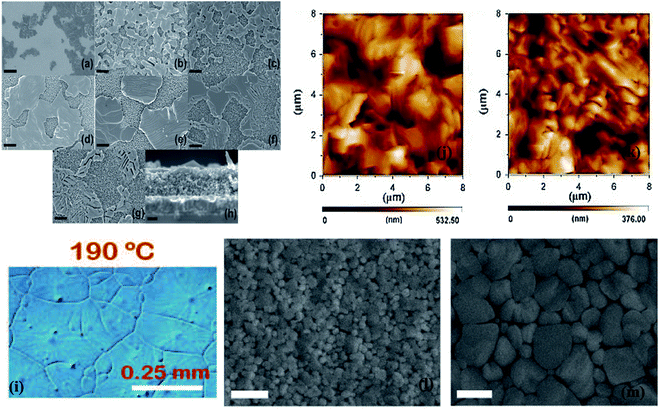 | ||
| Fig. 2 Scanning electron microscope images of m-TiO2 films with deposited perovskite solution heat-treated at different temperature (a) 60 °C, (b) 80 °C, (c) 100 °C, (d) 120 °C, (e) 150 °C, (f) 175 °C and (g) 200 °C. (h) Cross-sectional SEM image of the sample annealed at 150 °C. Black scale bars correspond to (a) 5 μm, (b–g) 1 μm, and (h) 200 nm. Reproduced by permission ref. 46, Copyright 2014 Wiley-VCH Verlag GmbH & Co. KGaA, Weinheim. Optical micrograph of CH3NH3PbI3–xClx perovskite thin film (i). Reproduced by permission ref. 47, Copyright 2015 American Association for the Advancement of Science. Atomic force microscopy images of perovskite thin films annealed with the one-step method (j), multi-step method (k). Reproduced by permission ref. 43, Copyright 2015 Elsevier B.V. Scanning electron microscope image of an unannealed hot-cast film (l) and an annealed hot-cast film (m), showing that the perovskite crystals grow during annealing. Reproduced by permission ref. 45, Copyright 2016 WILEY-VCH Verlag GmbH & Co. KGaA, Weinheim. | ||
L. Huang et al. reported the morphology and structure of perovskite films treated by two different annealing methods, one step (OS) direct annealing method and multi-step (MS) slow annealing method.43
Morphology of perovskites film has significantly improved in multi-step annealing method. Uniform films are obtained with complete coverage by MS annealing technique. The AFM images (Fig. 2j and k) show the surface morphology of perovskite films fabricated by MS method and OS method. Films obtained by MS method have low roughness with an RMS value of 35 nm whereas the film obtained by the OS method has a high roughness with an RMS value of 72 nm. By comparing the corresponding morphology and structure of the treated perovskite films, the author found that the MS method is a universal annealing procedure to realize highly efficient and well reproducible.43 Jacobus et al. have demonstrated a new, air-stable process technique for CH3NH3PbI3 perovskites.45 During this technique, a hot solution (70 °C) is applied on a preheated substrate and films was made by spin-coating in air. After then, the perovskites films are annealed between 80 °C and 100 °C temperature in ambient conditions. They recognized the varieties between the optimally annealed layer and the pristine hot cast layer. In Fig. 2l and m SEM image of unannealed and annealed hot-cast film is shown which reveals that perovskite crystal size increases during the post-deposition annealing. One thing is more observed that after annealing, chloride signals disappears that suggest that for removing excess salts annealing is a necessary step. The annealing environment effects a lot to perovskite film morphology. C. Wu et al. reported the low-pressure assisted technique with thermal annealing in double perovskite Cs2AgBiBr6 perovskite film fabrication.49 In this work, the spin coated film was quickly placed in a low-pressure chamber (20 Pa pressure) and after film was annealed at 200 °C. Due to this low pressure treatment before annealing, double perovskite film showed smooth and dense morphology in comparison to conventional thermal annealing method.
2.2 Effect of precursor aging
It was observed that precursor solution aging time has a subtle effect on the nucleation efficacy, thin-film formation, uniformity, and trap state density of the perovskite thin-film.50 All the above-mentioned aspects of film morphology determine the crystalline quality of the perovskite layer and hence the overall performance of the device. P. Boonmongkolras et al. demonstrated the correlation between perovskite precursor solution aging time and the triple cation perovskite Cs0.05(FA0.83MA0.17)0.95Pb(I0.83Br0.17)3 device performance.51 It was observed that devices which are fabricated from 6 hours aged solution show the maximum average efficiency with narrowest distribution and better reproducibility (Fig. 3a). The average grain was estimated similar in all the films but some voids were found along grain boundaries for the 168 hours and 720 hours aged precursor solutions. It was concluded that precursor solution which was aged longer than 6 hours reduced the device performance due to chemical inhomogeneity of the micron-sized colloidal intermediates. In conventional MAPbI3 PSC, this solution aging effect were not observed. | ||
| Fig. 3 (a) PCE distribution with precursor solution aging time (hours) of the triple-cation lead halide PSCs. Reproduced by permission ref. 51, Copyright 2018 Royal Society of Chemistry. (b) Photographs of triple cation (FA, MA, Cs) films produced from a fresh ink (viz., 0 days of storage, labeled as “Day 0”) and same ink is used for the 2–81 days storage. (c) Photographs of films which fabricated from 24 days old ink. Reproduced by permission ref. 52, Copyright 2018 American Chemical Society. | ||
The degradation mechanism in triple cation perovskite films was explained by B. Dou et al.52 In this work, perovskite ink used for fabrication of the films which contains the formamidinium (FA+), methylammonium (MA+), cesium (Cs+), lead (Pb2+), bromide (Br−) and iodide (I−). The photographs of perovskite films with storage days were shown in Fig. 3b and the photographs of perovskite films fabricated from 24 days old ink were shown in Fig. 3c. It was observed that the perovskite film appearance becomes visually lighter with the increased storage days. The perovskite film thickness and roughness were also effected by solution aging. The film thickness was enhanced from 542 ± 24 nm (on day 0) to 790 ± 84 nm (on day 81) with solution aging as well as becomes more rougher from 7 ± 1.5 nm on day 0 to 16 ± 3 nm on day 81 with ink aging. It was found that hydrolysis of DMF in the precursor solution forms dimethylammonium formate (DMA+), which incorporates in perovskite film along with a reduction of MA+ and Cs+ cations. These studies shows perovskite solution aging affects the perovskite morphology and device performance.
2.3 Effect of precursor temperature
PSCs are usually prepared with preheated perovskite solutions. G. Namkoong et al. tried to explore the underlying mechanism behind the influence of precursor solution temperature on PSCs.53 Perovskite (MAPbI3−xClx) solution was used after heating in a hot plate at various temperatures of 40 °C, 70 °C, and 90 °C for 24 h and thin films were coated by spin coating method in nitrogen gas-filled glove box.Fig. 4 shows the morphologies of CH3NH3PbI3−xClx films spin-coated on preheated glass slides at 180 °C with different precursor temperatures. The average grain size in the case of 70 °C-heated solutions is much larger than that of heated at 40 °C, but at 90 °C, there is a downfall in grain size. The solution temperature also has an effect on film thickness. The thickness of perovskite layers was investigated by cross-sectional scanning electron microscopy, and it was found as 210 ± 8 nm, 252 ± 7 nm, and 270 ± 6 nm at perovskite solution temperatures of 40 °C, 70 °C, and 90 °C respectively.
 | ||
| Fig. 4 Optical microscopic images of perovskite thin films with different perovskite solution temperatures of (a) 40 °C, (b) 70 °C and (c) 90 °C. Reproduced by permission ref. 53, Copyright 2016 Elsevier B.V. | ||
2.4 Effect of additives in perovskite precursor solutions
The commercialization of PSCs technology is essentially limited by the instability of MAPbI3 to water and ambient moisture. Hydrolyzation of CH3NH3PbI3 due to moisture is the main reason for perovskite degradation. Many attempts have been made to make perovskite processing and solar cells compatible with ambient humidity for large-scale production. Halide ion doping of perovskite, increasing hydrophobicity, and interfacial modification are the prominent methods of making perovskite-based solar cells compatible with ambient humidity.54–61 Various kind of additives has been added into perovskite precursor solution as an impactful way to enhance the film growth and formation with desirable surface morphology in PSCs. Li et al. explored a novel crystal cross-linking strategy to passivate the CH3NH3PbI3 perovskite grains with bifunctional organic molecule, butylphosphonic acid 4-ammonium chloride. This approach not only improved the performance of resulting PSCs but also rendered the devices highly immune towards the moisture.62 Chang Liu et al. used 4-tert-butyl pyridine (tBP) as an additive in CH3NH3PbI3 to increase the stability and performance of the solar cells fabricated in ambient condition with average relative humidity (RH) exceeding 40%.58 The tBP has a tertiary butyl group at one end, which makes the additive highly hydrophobic, and a hydrophobic layer is formed on the surface of MAPbI3 as a shield against humidity. Addition of tBP not only made the PbI2 and the upper perovskite layer hydrophobic but also a significant change in the film morphology. Fig. 5a–d shows the morphologies of the PbI2 and MAPbI3 films prepared with and without using of tBP additive, labeled as PbI2 W/O tBP (Fig. 5a), MAPbI3 W/O tBP (Fig. 5b), PbI2 W/tBP (Fig. 5c), and MAPbI3 W/tBP (Fig. 5d), respectively. It can be observed that PbI2 W/O tBP film is full of voids through which the underneath mesoporous TiO2 is visible and similar morphology of MAPbI3 W/O tBP. In contrast, PbI2 W/tBP and CH3NH3PbI3 W/tBP film are compact and pinhole-free. These results indicate the significant effect of tBP on the morphology of CH3NH3PbI3. The imparted hydrophobicity in the film reduced the corrosion of CH3NH3PbI3 by ambient moisture and pinholes. Morphology modification and moisture resistance of the perovskite layer induced by the tBP additive helps significantly in both improving device performance and stability of cells in the air. Fig. 5e shows a 20% fall in PCE of CH3NH3PbI3 W/tBP and complete degradation of CH3NH3PbI3 W/O tBP-based solar cells without encapsulation stored in the open air with the average RH level above 50% for over 7 days.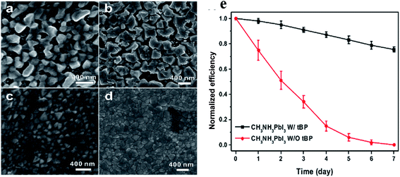 | ||
| Fig. 5 Scanning electron microscope images of PbI2 and MAPbI3 thin films (a and b) without tBP additive and (c and d) with tBP additive. (e) Evolution of the power conversion efficiencies of MAPbI3 with tBP and MAPbI3 without tBP-based solar cells with respect to time. Reproduced by permission ref. 58, Copyright 2017 American Chemical Society. | ||
M. Saliba et al. reported that the small and oxidation-stable rubidium cation (Rb+) can be embedded into a “cation cascade” to create perovskite materials with excellent material properties.63 Stabilized power conversion efficiency was achieved up to 21.6%. After coating the polymer on perovskite solar cell, it was observed that solar cell is stable around 500 hours at 85 °C (95% performance of its initial performance) under full illumination and maximum power point tracking. Detailed insights gained into the impact of Rb+ on the 3D perovskites amply brought out the absence of Rb+ from the lattice of various 3D perovskite structures, although, under similar experimental conditions, a certain amount of Cs+ was found to occupy the lattice.64 In fact, the presence of Rb+ in the precursor solution had a detrimental effect on the surface morphology, crystal structure and photophysical properties of CH3NH3PbI3 structures without even altering their bandgap. The increase in the photovoltaic performance of PSCs involving Rb+ and multiple-cation based compositions could be ascribed to positive interfacial effects associated with the formation of Rb+ based photoinactive phases.65,66 In a similar direction, using different sources of guanidinium cations, a significant improvement in terms of photovoltage (from 1.13 V to 1.20 V) was realized, which can be explained by evoking the reduction in the non-radiative recombinations and apparent gain in the charge carrier lifetime.67,68
Abdi-Jalebi et al. investigated the impact of adding small amount of monovalent cation halide based salts including NaI, CuBr, CuI, and AgI into the perovskite precursor solution on morphology, charge transport and optical properties of CH3NH3PbI3 perovskite.69 When NaI is added in the precursor solution, a huge change was observed in morphology of PbI2 overlayer. This overlayer of PbI2 contains branched large crystal and its surface is rough and porous.
In the presence of CuBr, there is no significant change in the morphology of PbI2 (Fig. 6b) while, in case of CuI and AgI based samples, a uniform, and pinhole-free overlayer are obtained (Fig. 6c and e). The right side of Fig. 6 displays top-view scanning electron microscope images of MAPbI3 films obtained after the conversion of pristine (Fig. 6a) and additive-based PbI2 films. In the pristine large tetragonal-shaped perovskite crystals formed on top of the mesoporous-TiO2 film while in CuBr based sample, the relatively better surface coverage of mesoporous-TiO2 with perovskite crystal is observed (Fig. 6b). In the presence of CuI and AgI additives, significant improvement in the surface coverage of titania scaffold with uniform and continuous perovskite structure is observed (Fig. 6c and e). In the case of AgI, the connectivity between perovskite crystals is better. In the case of NaI (Fig. 6d), large perovskite crystals with asymmetric shape are observed. The root-mean-squared roughness was estimated by atomic force microscopy and it was found for the pristine, CuBr, CuI, NaI, and AgI based perovskite films 51.2 nm, 28.2 nm, 21.3 nm, 63.0 nm, and 17.7 nm, respectively. In the presence of NaI additive perovskite film have branched morphology with the highest roughness while CuI and AgI based films have less roughness compared with the pristine sample. It was observed that CuI and AgI additives based perovskite films are nearly pinhole-free as compared to pristine and other samples. The confluence of aforementioned favorable properties led to the enhancement of power conversion efficiency to 15.14%, 15.25%, and 15.61% for NaI, CuI, and CuBr, respectively, in comparison with 14.01% for the additive-free reference cell. The photovoltaic results, particularly for AgI based cell, confirm that to achieving high efficiency, ideal surface coverage of perovskite is not the only sufficient factor but also a full conversion of lead iodide into the perovskite is required.
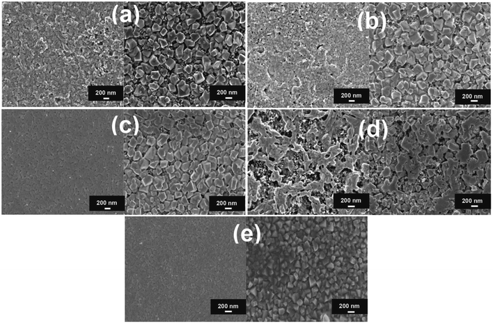 | ||
| Fig. 6 Top-view SEM images of PbI2 (left side) and CH3NH3PbI3 (right side) structures: (a) pristine, (b) CuBr, (c) CuI, (d) NaI, and (e) AgI based perovskite samples deposited on a mesoporous TiO2-coated FTO. Reproduced by permission ref. 69, Copyright 2016 Wiley-VCH Verlag GmbH & Co. KGaA, Weinheim. | ||
D. Bi et al. demonstrated a molecular design strategy to enhance morphology and photovoltaic performance of mixed-cation based FA0.9Cs0.1PbI3 perovskite solar cell.54 To achieve this goal, three imminent molecular modulators was designed, including thiol-based 5-(methylthio)-1H-tetrazole (S), ammonium-based anilinium iodide (N), and bifunctional 3-(5-mercapto-1H-tetrazol-1-yl)benzenaminium iodide (SN), that feature hydrophobic (hetero) aromatic cores functionalized by ammonium and thiol groups that can interact with explicit components of the perovskite phase and ensure abatement of the defects. It was found that by the molecular modulation strategy the perovskite grain size and crystallinity simultaneously enhances. The perovskite grain size is about 300 nm in the control film, and it increases up to 1 μm for the films containing either modulator S or SN. In the samples treated with SN modulator, a PCE 20.9% was achieved. This outstanding photovoltaic performance epitomizes the gainful impact of molecular modulation on the structure and morphology of perovskite films. This methodology unveils a generation of multifunctional molecular modulators (MMMs) with the capacity to advance PSC research and practical applications. M. Feng et al. built up a novel one-step solution approach utilizing methanol as an additive to produce high-quality perovskite films.22 It was observed that adding a proper amount of methanol into perovskite precursor solution not merely enhance the morphology and crystallinity of perovskite film, but enhance the optical and electrical properties of perovskite photoactive layer. Scanning electron microscopy was performed to investigate the morphologies of the perovskite films without and with (5 vol%) methanol (Fig. 7a and b). The perovskite film without methanol demonstrates small grains with apparent pinholes and grain boundaries. These deformities can introduce strong energetic disorder, impede charge transport, induce recombination and reduce photovoltaic performance. The addition of methanol can significantly enhance the morphology of perovskite film. The film with methanol has a superior surface roughness, larger grain size and fewer lateral grain boundaries than that without methanol. The grain size in the vertical direction of the film with methanol is comparable to the thickness of the film. This recommends that the charge carriers can efficiently transport across the perovskite film and reach the corresponding electrode interfaces before recombination. The fabricated planar perovskite solar cells with methanol have the highest PCE, which is 19.51% (Fig. 7c). More importantly, high-quality perovskite films with methanol also have high stability. Moreover, the power conversion efficiencies of devices with methanol are still high after kept in dark under ambient environment for 30 days. These outcomes give a new avenue for getting high efficiency, stable perovskite solar cells. H. Zheng et al. demonstrated the effect of DMSO amd thio-semicarbazide (TSC) additives on 2D perovskite (BA)2(MA)3Pb4I13 solar cell.70 It was observed that crystallization process regulates using these additives. The (BA)2(MA)3Pb4I13 two dimensional perovskite films were obtained as vertical-oriented. These 2D films have uniform morphology, increased grain size, intensified crystallinity and reduced trap state density. This 2D perovskite device have stability up to 720 hours in air atmosphere with relative humidity 25 ± 5% at 25 °C temperature.
 | ||
| Fig. 7 SEM images of perovskite films (a) without methanol and (b) with 5 vol% methanol. (c) Histogram of the PCEs of PSCs without and with (5 vol%) methanol. Reproduced by permission ref. 22, Copyright 2018 Elsevier Ltd. | ||
The presence of defect states and grain boundaries in perovskite film have deleterious effect on perovskite device performance. Defect passivation is a strategy to enhance the device efficiency and stability simultaneously.71–74 D. Xin et al. used 2-amino-5-cyanopyridine (ACP) molecule in perovskite precursor solution to passivate the defects located at grain boundary and surface through electrostatic interaction and the improved the performance of flexible PSCs.75 The reason of effective passivation of charged electronic defects is that ACP molecule have polar distributed electron density. Due to suppressed charge recombination and better charge extraction, a boost in efficiency was observed from 16.9% to 18.0%. J. Zhu et al. used 1,3,5-triazine-2,4,6-triamine (melamine) additive into PbBr2 precusor solution and fabricated high quality CsPbBr3 perovskite fims with lower grain boundary.74 It was observed that a combination formed between lead ions and melamine which produces void free perovskite film with loose grain size and less defect density. In melamine passivated films, suppressed recombination of charge carriers was observed due to better energy level matching. This inorganic perovskite device shows the superior stability with 85% RH over 720 hours. It was observed that charge carrier recombination can be suppressed and charge extraction can be enhanced using defect passivation strategy in perovskite solar cell which helps to produced highly efficient and stable perovskite solar cell.
2.5 Lewis acid–base adduct approach
The fabrication of highly efficient and long-term stable perovskite solar cell is critical for commercialization. Lewis acid–base adduct approach was developed for defect passivation, controlling grains in perovskite films, treating grain boundaries and for suppression of non radiative recombination.76–81 A Lewis acid with the capability of accepting a pair of nonbonding electrons has the capability to passivate electron-rich defects. J. Wang et al. reported highly efficient inorganic perovskite solar cell using a Lewis base and showed the suppressed non-radiative recombination.82 A schematic diagram of fabrication of CsPbIxBr3−x perovskite films with using passivation by lewis base 6TIC-4F shown in Fig. 8a. Perovskite films shows homogeneous surface morphology and average grain size increased from 110 nm to 200 nm after 6TIC-4F treatment. High efficiency 16.1% with improved photostability was achieved in this work. S. G. Ko et al. investigated the effect of thiourea on the perovskite crystallization.83 It is found that perovskite precursor solution penetrate better into the mesoscopic scaffolds after thiourea treatment. Without using thiourea perovskite precursor converts into rod like structure while after using thiourea perovskite precursor converted into ball-shaped crystals. Author revealed that this effect might be associated with the cross-linker function of thiourea. Another effect is that conversion of iodine molecule to I− ion can be reduced using thiourea, which will enhance the stability of perovskite film. Y. Zhao et al. reported the divalent hard Lewis acid doped CsPbBr3 films with 9.63% efficiency and ultra-stability.84 In this work, author doped Mg2+, Ca2+, Sr2+ and Ba2+ and optimized the doping dosage. It was found that the CsPb0.97Sr0.03Br3 have maximum PCE 9.63%, mainly attributed to the enlarged grain sizes and suppressed formation of point defect (vacancies) within perovskite films. The average grain size of the CsPb0.97Sr0.03Br3 film is enhanced significantly to 870 nm from 390 nm for the pristine CsPbBr3 film (Fig. 8b–f). This enhanced grain size is mainly attributed to the suppressed crystal nucleation formation.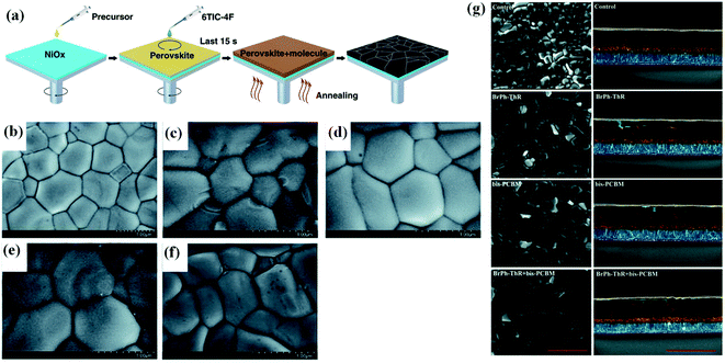 | ||
| Fig. 8 (a) Schematic diagram of the deposition processes of the prepared CsPbBrxI3−x perovskite film. Reproduced by the permission of ref. 82, Copyright 2020, Springer Nature. Top-view scanning electron microscope images of (b) CsPbBr3, (c) CsPb0.97Mg0.03Br3, (d) CsPb0.97Ca0.03Br3, (e) CsPb0.97Sr0.03Br3 and (f) CsPb0.96Ba0.04Br3 films. Reproduced by permission ref. 84, Copyright 2019 Royal Society of Chemistry. (g) SEM images. Top (left, the scale is 1 mm) SEM of corresponding perovskite films and cross-sectional (right, the scale is 2 mm) SEM of corresponding perovskite devices. (1) Control; (2) BrPh-ThR; (3) bis-PCBM; and (4) BrPh-ThR + bis-PCBM. Reproduced by permission ref. 85, Copyright 2018 Royal Society of Chemistry. | ||
L. Su et al. reported the π-conjugated Lewis base passivation of organic inorganic lead halide perovskites.77 The PCE was improved 24% by adding 3,30,5,50-azobenzene-tetracarboxylic acid (H4abtc) into the lead iodide (PbI2) precursor solution with Lewis acid–base adduct via two-step solution method. The device showed the superior stability in air, which efficiency can be retained 84% of its initial efficiency after 30 days. F. Zhang et al. observed the suppressed defects reported and produced highly efficient and stable perovskite solar cells.85 It was observed that grain size was increased and grain boundary reduces after using both BrPh-ThR and bis-PCBM (Fig. 8g). The combination of Lewis acid bis-PCBM and Lewis base BrPh-ThR enhances the crystallization, mobility and conductivity in perovskites. Using this combination, highest efficiency was achieved 21.7%. J. W. Lee et al. fabricated highly reproducible MAPbI3 perovskite solar cells with PCE as high as 19.7% via an adduct of PbI2 with oxygen donor DMSO.79 The adduct approach has been found to be adopted generally, where formamidinium lead iodide perovskite [HC(NH2)2PbI3 (FAPbI3)] with large grain, high crystallinity, and long-lived carrier lifetime is successfully fabricated via an adduct of PbI2 with thiourea as sulfur-donor Lewis base. D. Y. Son et al. treated the grain boundaries in CH3NH3PbI3 films using Lewis acid–base adduct approach.81 A CH3NH3I layer was formed at the grain boundaries by adding 6 mol% excess CH3NH3I to the precursor solution. Due to this excess layer at grain boundaries, non-radiative recombination was suppressed and electron–hole extraction boosted because of high ion conduction. By this grain boundaries healing process, I–V hysteresis significantly reduced and an average power conversion efficiency of 20.1% over 50 cells was achieved (best cell at 20.4%).
2.6 Post-device ligand (PDL) treatment
In a report, H. Zhang et al. presented the first sort of basic post-device ligand (PDL) treatment to significantly enhance the power conversion efficiency and stability of fully fabricated perovskite solar cells.86 In this work, diethylenetriamine (DETA) with three amine groups is employed as a ligand to treat perovskite solar cell. Specifically, ligand vapors are utilized to specifically treat the as complete prepared perovskite solar cell devices. Here DETA molecule can connect with MAPbI3 perovskite by substitution of the surface MA+ ion, resulting in an altered MAPbI3 or a stable non-MAPbI3 phase (e.g., layered perovskite). In Fig. 9a and b top view SEM image is shown and it was observed that there is no obvious change in grain size after PDL treatment. The control device without PDL treatment showed a power conversion efficiency of 18.67% and stabilized power conversion efficiency of 18.11%. In striking contrast, the device with PDL treatment demonstrated a significantly improved performance with a PCE of 20.13% and stabilized power conversion efficiency of 19.90%. The histograms of the device efficiencies are bestowed in Fig. 9c. | ||
| Fig. 9 Scanning electron microscope top view images of perovskite thin films (a) without any treatment and (b) with post-device ligand treatment. (c) Histograms of the perovskite device efficiencies with PDL treatment and without any treatment (37 cells were fabricated and tested). Reproduced by permission ref. 86, Copyright 2019 Royal Society of Chemistry. | ||
The PDL treatment considerably enhances the device reproducibility with a standard deviation of just 1.94% in power conversion efficiency that is over 220% increment over the control (without treatment) of 4.46%. Inexact eighty percent of the treated cells show power conversion efficiency above eighteen percent. The ligand vapors will initiate synthetic change in the selected lateral regions particularly that of the perovskite layer that prevents the diffusion of water molecules into the protected active perovskite region, so increasing the perovskite solar cell stability. In the interim, the stability of the treated devices without any exemplification amazingly enhances, with seventy percent efficiency kept up under ambient conditions after a five hundred hour maximum-power-point tracking test, whereas the control unencapsulated device will completely break down among one hundred hours.
2.7 Compositional engineering
Highly efficient and highly thermal stable perovskite solar cells production is a major challenge now because the efficiency of PSCs decreases at high temperature. By utilizing compositional engineering, the thermal stability of perovskites solar cells has been enhanced. Using mixed cation/halide approach highly efficient and stable PSCs devices have been reported.7,87,88 The cesium (Cs)–formamidinium (FA)–methylammonium (MA) triple cation-based perovskite device made-up in a glove box empowers reproducible high-voltage performance.89 In a work M. Saliba et al. used 3 cations, Cs, MA, and FA, to achieve highly stable and efficient PSCs.89 It was observed that when Cs is added to MA/FA mixtures then yellow phase impurities suppresses and uniform perovskite grains extends from the electron to the hole-collecting layer consistent with seed-assisted crystal growth. The Csx(MA0.17FA0.83)(100−x)Pb(I0.83Br0.17)3 triple cation based perovskite device gives stabilized power conversion efficiency exceeding 21% (Fig. 10a) and ∼18% following 250 hours (Fig. 10b) under operational conditions. These mixed triple cation perovskite films were found more thermally stable and less influenced by fluctuating surrounding factors like solvent vapors, heating protocols, and temperature. For reproducibility and large-scale fabrication of PSCs, this robustness of perovskite films is imperative. T. Singh et al. demonstrated the fabrication of highly efficient and stable solution-processable multi-cation PSC in ambient air and humidity-controlled method.88 The Cs/MA/FA perovskite film was spin-coated on top of the TiO2 scaffold layer and crystalline perovskite film formed with large grain size and whole surface coverage. The power conversion efficiency of this Cs/MA/FA perovskite solar cell was achieved above 20%.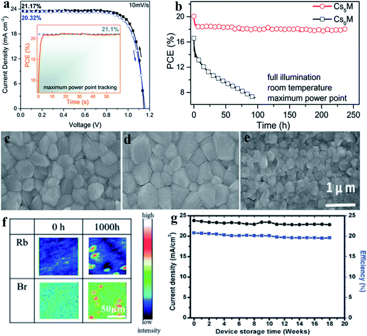 | ||
| Fig. 10 (a) I–V scan for Cs5M device that shows power conversion efficiency above 21% (b) change in device efficiency with time up to 250 hours of a high-performance Cs5M and Cs0M devices which kept in N2 atmosphere at room temperature with constant illumination and maximum power point tracking. Reproduced by permission ref. 89, Copyright 2016 Royal Society of Chemistry. Top view scanning electron microscope images of perovskite thin films made from (c) Cs0, (d) Cs5, (e) Cs10. Reproduced by permission ref. 88, Copyright 2017 Wiley-VCH Verlag GmbH & Co. KGaA, Weinheim. (f) Top-view TOF-SIMS elemental mapping of the Rb0.05Cs0.05FA0.75MA0.15Pb(I0.83Br0.17)3 perovskite thin film before and after thermal stress test at 85 °C for 1000 h. Reproduced by permission ref. 90, Copyright 2019 Wiley-VCH Verlag GmbH & Co. KGaA, Weinheim. (g) Current density and efficiency change with device storage time in weeks. Reproduced by permission ref. 88, Copyright 2017 Wiley-VCH Verlag GmbH & Co. KGaA, Weinheim. | ||
In Fig. 10c–e SEM top view image is shown of triple cation perovskite films with a variation of Cs Concentration. It was observed that morphology and grain size of Cs/MA/FA perovskite thin film is highly influenced by Cs concentration under the ambient air process, and Cs5% device gives the best performance with micrometer grain size (Fig. 10g). The device is highly stable and retained high efficiency (PCE = 19.5%) up to eighteen weeks. T. Matsui et al. explained in a report that the addition of Rb and the halide composition of the perovskite absorber layer affects the thermal stability of perovskite solar cells.90Fig. 10f shows the top-view TOF-SIMS elemental mapping of the Rb0.05Cs0.05FA0.75MA0.15Pb(I0.83Br0.17)3 perovskite thin film before and after thermal stress test at 85 °C for 1000 h. The solar cell device before the test demonstrated a state-of-the-art efficiency of 20.6% (20.1% stabilized efficiency). After testing, the power conversion efficiency of the device was still 19.0% (18.5% stabilized efficiency), which corresponds to 92% retention. The average efficiencies of four devices also showed good stability, with 20.4% initial efficiency, 18.7% efficiency after 1000 h of testing, and 92% retention. In perovskite solar cells instability against thermal stress and humidity is a major issue.
Abdi-Jalebi et al. investigated the effect of potassium passivation on halide perovskites.91 In another report, Abdi-Jalebi et al. investigated the moisture stability and the local chemistry of the passivated triple cation perovskite thin films.92 The perovskite films were stored under elevated humidity conditions (50% RH) in the nitrogen gas for a period of twenty-four hours. The morphology of the triple cation and Rb- and K-passivated triple cation perovskite films was investigated before (Fig. 11a–c) and after (Fig. 11d–f) this humidity treatment.
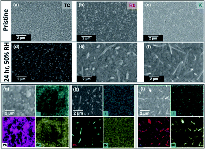 | ||
| Fig. 11 Scanning electron microscope top-view images of pristine (top row) and with 50% relative humidity, nitrogen over a course of twenty-four hours (second row) (a and d) triple cation, (b and e) Rb-passivated triple cation, and (c and f) K-passivated triple cation perovskite thin films. SEM image with EDX elemental mapping of the same (g) triple cation, (h) Rb-passivated triple cation and (i) K-passivated triple cation perovskite thin films. Reproduced by permission ref. 92, Copyright 2018 American Chemical Society. | ||
In all the unexposed perovskite films grain size was observed ∼200 to 400 nm with uniform packing (Fig. 11a–c). After humidity exposure for twenty-four hours, it was observed that some material is formed on the surfaces of all thin films. The author proposed that the surface material for the triple cation specimen corresponds primarily to PbI2, which is particularly abundant at the GBs (Fig. 11d and g). This is similar to degradation in other polycrystalline materials where grain boundaries are centers for degradation, often called intergranular degradation. Based on SEM-EDX analysis, some needle-like long crystals (≥30 μm) were found, that are rich in Cs. Furthermore, it was observed that the formation of Rb-rich crystals in Rb-passivated TCs, which appear to be primarily rich in I but also smaller fractions of Br (Fig. 11e and h). Finally, it was observed that the formation of KBr-rich surface crystallites in the K-passivated TC films after the humidity treatment, which has a similar composition as those in cross-sectional STEM-EDX decomposition profile but is of larger size and distributed across the surface (Fig. 11f and i). These results suggest that moderate humidity exposure promotes the formation of non-perovskite material in each of the film compositions, with the composition of the non-perovskite material being consistent with that observed at elevated loadings of additives. Interestingly, the author observed a significant coalescence of small perovskite grains into larger “fused” domains in the perovskite thin films upon 50% RH treatment in the TC and K-passivated TC (Fig. 11a, d, c and f). It was found that the average grain size increases remarkably from ∼200 nm to ∼2 μm in both samples for grain size distributions. Zhifang Wu et al. fabricated a stable perovskite solar cell by combining thermally stable formamidinium-cesium-based perovskite and a moisture-resistant carbon electrode.19 This perovskite solar cell maintain on average 77% of the initial efficiency value after being aged for 192 h under conditions of 85 °C and 85% relative humidity without encapsulation.
2.8 Interface engineering
Interface engineering in organo-metal halide perovskite solar cells (PSCs) has been an effective tool to enhance the photovoltaic performance and stability of photovoltaic (PV) devices.18,19,55,93–98 It is renowned that zinc oxide (ZnO) is one in all promising electron transporting layers for solar cells and is additionally applicable for flexible devices. Nevertheless, the usage of ZnO in perovskite solar cells is limited because it reacts with the perovskite film amid the annealing procedure. M. M. Tavakoli et al. demonstrated a perovskite device using a modified electron transport layer with a power conversion efficiency 20.94% (Fig. 12a and b). A monolayer of graphene is introduced at the interface of the ZnO ETL and perovskite absorber.99 This perovskite device keeps up over 80% of its initial efficiency value after 300 hours under continuous illumination. Strikingly, author observed that the introducing a monolayer of graphene at the ETL/perovskite interface enhances the carrier extraction and photovoltaic properties and addition shields the perovskite film from decay at elevated temperatures, which is gainful for the stability of the device. To enhance the stability considerably more, the surface of the perovskite film is passivated by utilizing another modulator, i.e., 3-(pentafluorophenyl)-propionamide (PFPA) to abate the surface trap states of the perovskite. In view of this change with MLG and PFPA, a stable perovskite solar cell device with a power conversion efficiency of twenty-one percent was accomplished under AM1.5G illuminations with insignificant hysteresis. The stability result shows that the passivated device on MLG/ZnO keeps up 93% of its initial PCE value after 300 h under continuous illumination (Fig. 12c). In another report, the author investigated the effect of adding MACl on triple A-cation perovskite films. It was found that bulk and surface defects in perovskites are suppressed and high-quality films with large grain size are obtained.100 There is a dramatic enhancement in the grain size from 200 to more than 1000 nm after adding this MACl additive.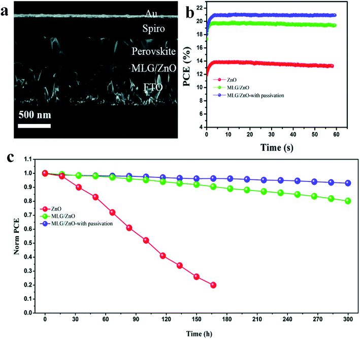 | ||
| Fig. 12 (a) Cross-sectional SEM image of the PSC device based on MLG/ZnO. (b) Power conversion efficiency curve with time under maximum power point tracking. (c) Stability test of perovskite solar cell devices based on ZnO, MLG/ZnO, and MLG/ZnO-with passivation under continuous illumination for 300 hours at room temperature and under nitrogen flow. Reproduced by permission ref. 99, Copyright 2019 Royal Society of Chemistry. | ||
After applying these modifications, maximum efficiency was obtained 21.65% and open-circuit photovoltage was achieved 1.24 V with a 370 mV loss. Furthermore, the defect healing improves the operational stability of the perovskite devices that retain 96%, 90%, and 85% of their initial PCE values after 500 h under continuously light illumination at 20 °C, 50 °C, and 65 °C, respectively. X. X. Gao et al. demonstrate that using the conjugated polymers (PD-10-DTTE-7) with both the donor and acceptor alkylated as an interlayer between MAPbI3 and doped Spiro-OMeTAD can significantly increase the performance of MAPbI3 solar cells.55 Atomic-force microscopy (AFM) analysis reveals that the determined roughness value was 24.6 nm for MAPbI3 film and 16.3 nm for PD-10-DTTE-7/MAPbI3 film. With the tailored interface, the MAPbI3 solar cells with PD-10-DTTE-7 interlayer shows the best power conversion efficiency of 18.83%.
Abdi-Jalebi et al. demonstrated that thermally evaporated dopant-free tetracene (120 nm) on top of the perovskite layer, capped with a lithium-doped Spiro-OMeTAD layer (200 nm) and top gold electrode, offers an excellent hole extracting stack with minimal interfacial defect levels.101 For a perovskite layer interfaced between these graded HTLs and a mesoporous TiO2 electron-extracting layer, its photoluminescence yield reaches 15% compared to 5% for the perovskite layer interfaced between TiO2 and Spiro-OMeTAD alone. The surface morphologies of different layers were investigated using a top-view SEM at different magnifications. In Fig. 13A–C shows that tetracene and perovskite films are compact polycrystalline with micrometer grain size while Spiro adopts a conformal coating (Fig. 13D), ensuring total surface coverage of the combined HTLs. For perovskite solar cells with a graded hole-transport layer structure, the power conversion efficiency was achieved 21.6% and an extended power output of over 550 hours of continuous illumination at AM1.5G, retaining more than 90% of the initial performance. J. Lu et al. built up a facile technique to improve the PCE and generously upgrade the stability of perovskite solar cells via modification of the interface between the light-harvester and the hole transporting layers with benzenethiol dipoles.102 Highest power conversion efficiencies of 20.2% for the small area devices (0.16 cm2) and 19.6% for the PSCs with an active area over 1 cm2 under 1 sun AM1.5G irradiation were accomplished with solar cells modified with HS-Ph-CN. Under simulated solar cell working conditions (1 sun AM1.5G irradiation, 50% RH, 50 °C device temperature), such devices retained more than 80% of their initial photovoltaic performance after 50 h and operated stably over the following 135 h. The interfaces on either side of the hole conductor were investigated to further improve the performance and stability of PSCs. By the introduction of thin layer of reduced graphene oxide layer between CuSCN, an inorganic hole conductor, and Au-back contact, the potential-induced degradation effects were completely mitigated leading to the realization of highly-stable PSCs yielding efficiencies greater than 20%.103 To further improve the performance and moisture stability of PSCs, a highly hydrophobic a two-dimensional (2D) A2PbI4 perovskite layer using pentafluorophenylethylammonium (FEA) as A-cation, was introduced between iodide-based perovskite layer and Spiro-MeOTAD. The efficiency of the resulting solar cells exceeded 22% value.104
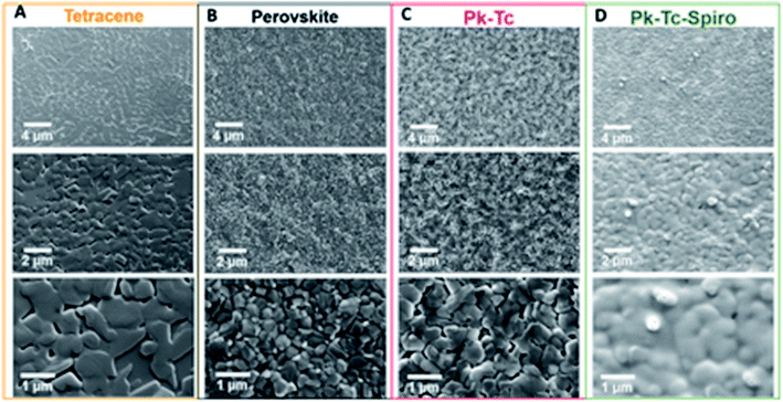 | ||
| Fig. 13 Top-view scanning electron microscopy of (A) tetracene (Tc) single layer, (B) perovskite (Pk), (C) perovskite–tetracene (Pk–Tc), and (D) perovskite–tetracene–Spiro (Pk–Tc–Spiro) films at three different magnifications. Reproduced by permission ref. 101, Copyright 2018 American Association for the Advancement of Science. | ||
2.9 Solvent engineering
To improve the perovskite solar cell device performance, it is necessary to control the film formation kinetics and crystallization during perovskite deposition. The morphology of perovskite film can be optimized by controlling nucleation and crystal growth, for this purpose solvent engineering is a very viable strategy.105–107 Y. Zhou et al. employed an antisolvent–solvent extraction process for crystallization behavior of mix halide perovskites at room temperature (Fig. 14a).108 In this strategy, a little amount of solvent diffuses within the large amount of antisolvent. For the crystallization procedure, super-saturation state and nucleation are accomplished by this antisolvent–solvent extraction method and nucleation rate may be improved by the magnetic stirring of antisolvent. DEE (anhydrous diethyl ether) was used as antisolvent and in the antisolvent bath, advection was introduced by using magnetic stirrers. MAPbI2Br and MAPbIBr2 perovskite thin film were formed. For the investigation of surface morphology of perovskite thin-film scanning electron microscopy (SEM) and atomic force microscopy (AFM) was performed. In without stirred case grain size was found ∼100 nm to ∼250 nm and in stirred case, the grains size was found approximate 100 nm. The overall roughness of thin film formed by both method without and with stirring is approximate similar ∼9 nm. In stirred case, the morphology of MAPbIBr2 perovskite film is improved in comparison to without stirred case. In stirred case, surface coverage is improved and the compact film is formed while in without stirred case, perovskite film has big gaps between micron-sized large grains. The roughness is also decreased from ∼160 nm (without stirred) to ∼15 nm (stirred). The antisolvent–solvent extraction process is a simple methodology for the fabrication of perovskite films with high quality and improved morphology. In our group, A. Raghav et al. developed a straightforward strategy to produce uniform perovskite film utilizing a dual solvent elimination method (DSEM) at room temperature.109 In Fig. 14b, the schematic diagram of the DSEM technique is shown. In this work, two solvents were used with a huge difference in dielectric constant. The dielectric constant of DMF and DEE is 36.7 and 4.3 respectively. The large difference in dielectric constant makes a difference in solubility. The author observed that perovskite thin film produced by this DSEM technique has uniform film coverage and average grain size is 500 nm. In Fig. 14c AFM image is shown of CH3NH3PbI3 perovskite film which reveals that the RMS value of surface roughness of perovskite film was observed approximate 7 nm. Using the DSEM, by tuning solvent dielectric constants, author found a uniform CH3NH3PbI3 perovskite thin film with optimized morphology. This DSEM approach as delineating here gives a novel strategy of optimizing morphology in organic–inorganic halide PSCs. M. Xiao et al. demonstrated a fast, single-step, solution-based deposition crystallization technique which allows control over the dynamics of nucleation and grain growth of CH3NH3PbI3, and achieves the rapid and reproducible fabrication of high-quality perovskite thin films.24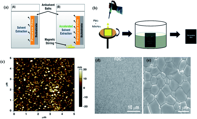 | ||
| Fig. 14 (a) Schematic delineation of the crystallization process of perovskite in the antisolvent bath: (A) standard process without stirring; (B) accelerated process with magnetic stirring. Reproduced by permission ref. 108, Copyright 2016 American Chemical Society. (b) The schematic diagram of the DSEM technique. (c) AFM image of DSEM fabricated perovskite film. Reproduced by permission ref. 109, Copyright 2017 Elsevier B.V. SEM images of the surface of a MAPbI3 film prepared by FDC with the addition of chlorobenzene (d) low magnification and (e) high magnification. Reproduced by permission ref. 24, Copyright 2014 Wiley-VCH Verlag GmbH & Co. KGaA, Weinheim. | ||
In this approach, a DMF solution of CH3NH3PbI3 perovskite is spin-coated on a substrate, followed immediately a second solvent introduced on top of the wet film during the spin coating process, like chlorobenzene (CBZ) to induce fast crystallization. The second solvent plays a crucial role to reduce the solubility of CH3NH3PbI3 and promoting fast nucleation and growth of the crystals within the thin film. Fig. 14d and e shows the low and high magnification SEM image of the perovskite films. The perovskite films formed by the FDC process shows full coverage of surface and consists of micron-sized grains. It was observed that the perovskite film have large crystalline grains and perovskite film is free of grain boundaries.24 J. Liu et al. reported effective and stable green mixed anti-solvent engineering for inverted planar perovskite solar cells.106 The surface morphology of perovskite films could be enhanced and grain boundary of perovskite thin film could be passivated by this green mixed anti-solvent technique. Therefore, the photovoltaic performance of p–i–n planar perovskite solar cell significantly increased. The power conversion efficiency of 18.98% with no hysteresis was achieved for the best performing device. The device has praiseworthy stability over 30 days in dry conditions.
Kun-Mu Lie et al. reported the effect a various mixture of anti-solvent on perovskite precursors, which enhance the crystallinity and surface morphology of the MAPbI3 active layer.105 The perovskite film treated with toluene (TL) mixed with dichlorobenzene (DCB) in an equal volume ratio has the best film quality and power conversion efficiency of 18.01%. All bromide-based perovskite materials hold great potential primarily to obtain high photovoltages, which could be exploited in driving the various non-feasible electrochemical reaction, e.g., water splitting, and carbon dioxide reduction.110 Various approaches have been employed to improve the photovoltage of bromide perovskite-based solar cells.111 Towards this end, a mixture of solvents including DMF and DMSO were used to deposit highly contiguous PbBr2 layer onto mesoporous TiO2 layer.112 Subsequently, there lead bromide layers were converted into FAPbBr3 layers exhibiting exceedingly slow charge-carrier recombination dynamics, low energetic disorder, less non-radiative recombination, and highly PLQY, which eventually translated into remarkable photovoltages greater than 1.5 V.113,114 G. Liu et al. reported the solvent induced morphology control in two dimensional (BA)2(MA)3Pb4I13 perovskites.115 In this work, DMF and GBL solvents used for the fabrication of films. In DMF processed film lot of pin holes were observed while in GBL processed film uniform and condensed morphology with full coverage was obtained. The device efficiency was increased to 13.9% in GBL processed device in comparison to DMF processed device (9.81%).
2.10 Solvent vapor annealing
Solvent vapor annealing of perovskite films during a controlled environment has been utilized as a technique by numerous researchers to enhance the grain size, crystallinity and thereby achieving highly efficient solar cells.23,116–118 The challenge in solvent vapor annealing is the retaining of excessive residual solvent within the film that is destructive to the device performance. The presence of excess residual solvent can be avoided by appropriately modifying the morphology of PbI2 and uniform perovskite films can be acquired. This happens despite the fact that compact amorphous PbI2 prompted to form compact perovskite films where the grain size remains only around 200 the nm. T. Liu et al. designed mesoporous PbI2 scaffold first by controlled nucleation and growth mechanism and then obtained a highly-crystalline perovskite film.119 Therefore, correlations between the PbI2 film morphology and solar cell performance could be established. Z. Xiao et al. observed that annealing of solvent can impact the crystallinity and grain size of the perovskite film.23Fig. 15a–i shows the SEM top surface images and grain size distributions of the thermally annealed and solvent annealed CH3NH3PbI3 perovskite films. It was observed that the average grain size in perovskite films enhances uniformly in all directions. In the solvent annealed perovskite films grain size expanded linearly with the film thickness up to one micrometer and in thermally annealed films maximum grain size was solely around 260 nm. The highest device PCE of solvent annealed PSC was found 15.6% at 630 nm thickness and device efficiency stayed above 14.5% as the perovskite thickness increased to 1015 nm. H. Xiong et al. demonstrate a low-priced and straightforward two-step deposition technique to produce compact and high crystalline films.117 In this work firstly a high quality, well oriented and crystallized film of PbI2 was produced utilizing a vapor post-annealing strategy in ambient conditions. This PbI2 film converts into a compact, large grain size, pinhole-free CH3NH3PbI3 film under ambient conditions. The CH3NH3PbI3 film morphology that resulted from the mesoporous precursor was uniform as confirmed by AFM images. These results demonstrate the importance of morphology control in the PbI2 phase for high-performance perovskite solar cells fabricated under ambient conditions. The straightforward strategy exhibited here could be utilized to prepare large-area perovskite solar cells in ambient conditions. J. Liu et al. investigated the impact of annealing treatment of perovskite films under different atmospheric conditions on the crystallinity of perovskite films.116Fig. 16 delineates the schematic diagram of the annealing treatment of perovskite films under solvent vapor. In this report, five atmospheres N2, H2O, γ-butyrolactone (GBL), DMF, dimethyl sulfoxide (DMSO) were used to examine the influence of different annealing atmospheres on MAPbI3 perovskite films. In Fig. 17a–e SEM images show the morphology of perovskite film after annealing under different solvent vapor. The author observed that after annealing in DMSO atmosphere, the voids disappear and perovskite film shows good crystallinity with grain size exceeding its film thickness. The variety in morphology and crystallinity in the perovskite films would be expected due to differences in coordinating capability and vapor pressure of the three solvents GBL, DMF, and DMSO. The vapor pressure at room temperature (20 °C) is 1.5, 2.7, and 0.42 mmHg for GBL, DMF, and DMSO, respectively, which is predictable with the pattern of grain size of perovskite films. Since solvent DMSO has low volatility because of its relatively high boiling point (189 °C) and low saturated vapor pressure, it is very likely that the DMSO vapor environment may be maintained in a long time and thus results in remarkable film growth.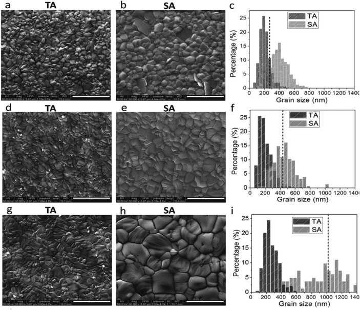 | ||
| Fig. 15 Scanning electron microscope images of the thermally annealed (TA) perovskite films with thicknesses of 250 nm (a), 430 nm (d), and 1015 nm (g), and solvent-annealed (SA) perovskite films with thickness of 250 nm (b), 430 nm (e) and 1015 nm (h); the scale bars in the SEM micrographs are 2 μm. (c, f and i) Grain-size distributions of the SEM images to the left. Reproduced by permission ref. 23, Copyright 2014 Wiley-VCH Verlag GmbH & Co. KGaA, Weinheim. | ||
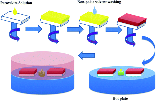 | ||
| Fig. 16 Schematic diagram of the annealing treatment of perovskite films under solvent vapor. Reproduced by permission ref. 116, Copyright 2015 American Chemical Society. | ||
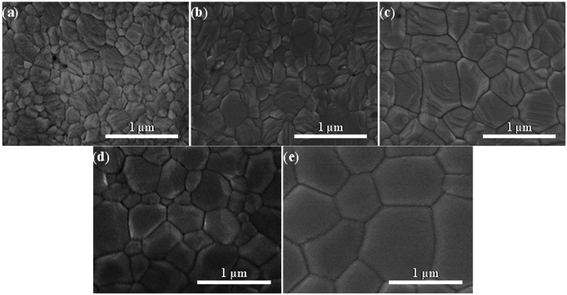 | ||
| Fig. 17 Surface SEM images of perovskite films on ITO-coated substrate after annealing under different atmospheric conditions: (a) N2, (b) H2O, (c) GBL, (d) DMF, (e) DMSO. Reproduced by permission ref. 116, Copyright 2015 American Chemical Society. | ||
2.11 Impact of deposition methods
Halide perovskite thin film morphology includes two main precursor components relies upon the deposition route. It can be solution processable or vacuum-based deposition. The precursors can be deposited simultaneously or independently. So there are many deposition methods to produce perovskite thin films. In this section we have discussed some solution-processable deposition methods of perovskites films and their effect on morphology and efficiency of perovskite solar cells.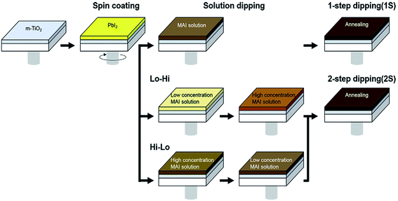 | ||
| Fig. 18 Schematic diagram of the fabrication process of CH3NH3PbI3 perovskite films. Here 1S means one-step MAI dipping as conventional sequential deposition process and 2S means two-step MAI dipping by changing MAI concentration as Lo–Hi and Hi–Lo. Reproduced by permission ref. 126, Copyright 2016 Elsevier B.V. | ||
In the case of one step dipping, lower concentrated MAI solution (6 mg of MAI per 1 mL of IPA) creates a sparse and uneven coverage of the film while a higher concentration of MAI solution (10 mg of MAI per 1 mL of IPA) creates dense CH3NH3PbI3 perovskite film but with remnant un-reacted PbI2 as detected by XRD data. In the case of two steps dipping, dense and rough crystals were formed for the Lo–Hi sequence. In the case of two steps dipping process, the first treatment in low concentrated MAI solution allowed to form few nuclei and thus it becomes easier for the second high concentrated MAI solution to react with the inside PbI2 layer.
In the reverse case (2S Hi–Lo), the first dense MAPbI3 layer is formed due to the high concentration of MAI solution, which then hinders the low concentrated MAI to diffusion into the PbI2 layer. Thus CH3NH3PbI3 perovskite crystals aggregate on top of the CH3NH3PbI3 thin film and conversion of PbI2 remain incomplete. A solar cell made from 2S Lo–Hi perovskite layer reported to shows best performance with an average PCE of 15.1%, high reproducibility, and stability than the others. This is due to increased Jsc due to light scattering effects and the contact area between the MAPbI3 and the adjacent layer of Spiro-OMeTAD. In a similar direction, instead of pure PbI2, a mixture of lead halide salts was employed to achieve precise control over the morphology and optoelectronic properties of resulting perovskite layer. The addition of chloride salt, irrespective of the source, seems to greatly influence the formation and growth of chloride-free CH3NH3PbI3 structures.127 Specifically, the introduction of 2 mole% of PbCl2 or 1 mole% of PbBr2 into PbI2 precursor solution leads to the realization of remarkable improvement in the photovoltaic performance of PSCs without altering the bandgap of the light-absorbing layer.128,129 Authors also unraveled that PbCl2 majorly improves the photovoltage of the devices, associated with desired charge-carrier recombination dynamics, whereas PbBr2 enhances both photocurrent density and photovoltage of the devices.
Y. Y. Kim et al. proposed a new two-step processing strategy, to be specific, mediator extraction treatment (MET), reasonable for a large-area, rapid roll-to-roll process (Fig. 19a).130 In this work a PbI2-DMSO film was first deposited and for extract the DMSO this PbI2-DMSO film was dipped in a 2-propanol bath. The transparent film turns a hazy yellow within a few seconds. This yellow PbI2 film dipped in MAI solution and dark-brown MAPbI3 film formed. The morphology of perovskite films was investigated by scanning electron microscopy. The PbI2-DMSO film had smooth morphology (Fig. 19b) while after washing DMSO mediator with IPA the film morphology becomes porous (Fig. 19c). The porous PbI2 film reacts rapidly with MAI molecules and converts in uniform, pin-hole-free and dense MAPbI3 perovskite film within several minutes (Fig. 19d). The power conversion efficiency of corresponding solar cells was achieved by 18.8% under optimum conditions.
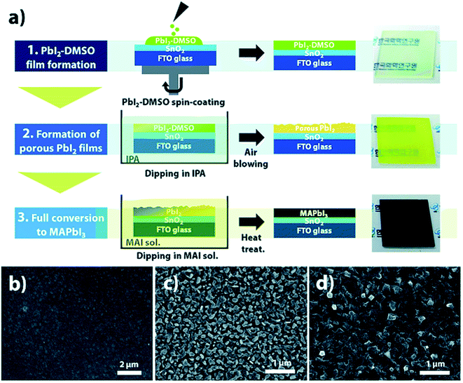 | ||
| Fig. 19 (a) Schematic diagram of mediator extraction treatment (MET) representing each step and optical images of the resulting perovskite films. The scanning electron microscope images of (b) PbI2-DMSO, (c) PbI2, and (d) MAPbI3 films fabricated by MET. Reproduced by permission ref. 130, Copyright 2018 Royal Society of Chemistry. | ||
C. Yi et al. presented a new and effective strategy to produce high-quality perovskite films by a sequential deposition technique, in which a PbX2 capping layer is introduced that is invested with a network of interconnected nanopores.131 In this report, a mesoporous PbX2 film was prepared onto a nanocrystalline TiO2 scaffold. This highly porous PbX2 layer covers the nanocrystalline TiO2 scaffold. The interconnected mesopores serve as channels to allow for rapid infiltration by the solution of the reagents and provide a large internal surface area, enhancing the insertion of the organic ammonium halides into the lead halide lattice, resulting in rapid and quantitative conversion to perovskite. They produced the required continuous and dense perovskite capping layer consisting of FA1−xMAxPb(I1−xBrx)3. The best power conversion efficiencies (PCEs) were achieved 20.4% with negligible hysteresis in their J–V curve (Fig. 20a). Qi Li et al. reported a perovskite seeding growth (PSG) method and CsCl-enhanced PbI2 precursor method to incorporate cesium cations into FAPbI3-based low-bandgap perovskite film through a sequential deposition.132 To investigate the difference between the films morphology the scanning electron microscopy experiment was carried out. It was observed that grain size is twice larger with CsCl in comparison to without CsCl (Fig. 20b and c). The introduction of CsCl and perovskite seeds into PbI2 layer together led to a larger perovskite crystal, grain size, better crystalline quality, less grain boundaries, fewer defect states, and long carrier lifetime. The power conversion efficiency of perovskite solar cell with CsCl-enhanced PbI2 precursor method was achieved to be 22.1% (Fig. 20d).
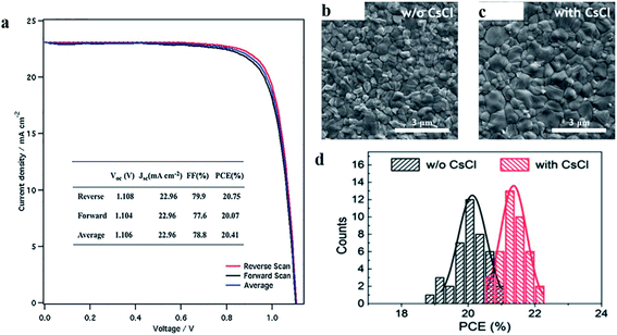 | ||
| Fig. 20 (a) J–V curves of best performing perovskite solar cell devices. Reproduced by permission ref. 131, Copyright 2016 Wiley-VCH Verlag GmbH & Co. KGaA, Weinheim. Scanning electron microscope top-view image of perovskite film fabricated by (b) PSG method and (c) CsCl-enhanced PbI2 precursor method. (d) Histogram of solar cell efficiencies with Gaussian function fitting in reverse scan for 40 devices. The black curve is for without CsCl and the red curve is for with CsCl in eight batches. Reproduced by permission ref. 132, Copyright 2018 Wiley-VCH Verlag GmbH & Co. KGaA, Weinheim. | ||
![[thin space (1/6-em)]](https://www.rsc.org/images/entities/char_2009.gif) :
:![[thin space (1/6-em)]](https://www.rsc.org/images/entities/char_2009.gif) MA molar ratio of 2
MA molar ratio of 2![[thin space (1/6-em)]](https://www.rsc.org/images/entities/char_2009.gif) :
:![[thin space (1/6-em)]](https://www.rsc.org/images/entities/char_2009.gif) 3 in the precursor solution as compared to FA
3 in the precursor solution as compared to FA![[thin space (1/6-em)]](https://www.rsc.org/images/entities/char_2009.gif) :
:![[thin space (1/6-em)]](https://www.rsc.org/images/entities/char_2009.gif) MA molar ratio of 0.8
MA molar ratio of 0.8![[thin space (1/6-em)]](https://www.rsc.org/images/entities/char_2009.gif) :
:![[thin space (1/6-em)]](https://www.rsc.org/images/entities/char_2009.gif) 0.2, where big gaps are presented between grains. The power conversion efficiency of the FA0.4MA0.6PbI3 perovskite device was achieved 18.3% and stability longer than thirty days in the air for the unsealed devices.
0.2, where big gaps are presented between grains. The power conversion efficiency of the FA0.4MA0.6PbI3 perovskite device was achieved 18.3% and stability longer than thirty days in the air for the unsealed devices.
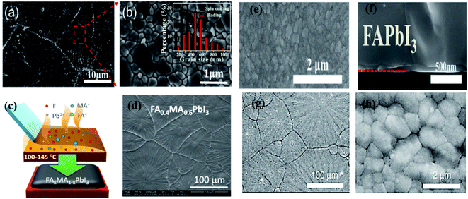 | ||
| Fig. 21 (a) Scanning electron microscope images of doctor-bladed CH3NH3PbI3 film fabricated at 130 °C. (b) Scanning electron microscope images of the selected area in (a). The grain size distribution of CH3NH3PbI3 films is shown in the inset. The red color is for the doctor-bladed and black color is for spin-coated films. Reproduced by permission ref. 142, Copyright 2017 Elsevier B.V. (c) Diagram of the doctor-blade coating for the fabrication of mixed cation perovskite film. (d) SEM images of FA0.4MA0.6PbI3 perovskite films fabricated by doctor-blade technique. Reproduced by permission ref. 143, Copyright 2016 Wiley-VCH Verlag GmbH & Co. KGaA, Weinheim. (e) SEM surface image and (f) cross-sectional SEM image of α-FAPbI3 films fabricated via doctor-blading. Reproduced by permission ref. 144, Copyright 2017 Elsevier B.V. SEM images of bladed and doped CH3NH3PbI3 perovskite film (g) low magnification and (h) high magnification. Reproduced by permission ref. 145, Copyright 2018 Springer Nature. | ||
S. Li et al. demonstrated the fabrication of FA-based perovskite films by doctor blading strategy in ambient condition.144 In this work high-purity, black α-phase formamidinium lead iodide (FAPbI3) perovskite polycrystalline film was fabricated without further annealing procedure and any additives. The substrate temperature was optimized at 170 °C for the formation of continuous FAPbI3 film. SEM surface image shows that the produced FAPbI3 film has good surface coverage and a pin-hole free film formed rapidly with excellent coverage (Fig. 21e). The perovskite film is comprised of large-size grains and therefore the cross-section image (Fig. 21f) demonstrates that the grains can connect very well without obvious grain gap in which the photon-generated carrier could transfer freely with low recombination. W. Q. Wu et al. employed a molecular-doping technique for a perovskite layer to doctor-blade HTL-free PSCs. Here MAPbI3 perovskite precursor dissolved in DMF containing p-type dopant 2,3,5,6-tetrafluoro-7,7,8,8-tetracyanoquinodimethane (F4TCNQ) was dripped onto substrates that were heated at 150 °C, followed by a quick blading procedure to spread the solution onto the substrates.145 The perovskite domains were densely packed together, and without observable voids at domain boundaries (Fig. 21g and h). It should be noted that these domains don't seem to be single crystalline grains. Every micrometer-scale convection domain was comprised of micron-sized grains extending from 800 to 1700 nm. By utilizing a bladed and doped MAPbI3 film as the photoactive layer in an HTL-free device structure, a stabilized PCE 20.2% with almost no J–V hysteresis is obtained (Fig. 22a). Shi Tang et al. reported composition engineering in doctor-bladed OIHP solar cells.146 In this work, a little fraction of Cs+ cations and Br− anions were introduced into (MAPbI3)0.6(FAPbI3)0.4 mixed precursor solution and a pinhole-free and smooth perovskite MA0.6FA0.38Cs0.02PbI2.975Br0.025 film were produced via doctor blade coating at a lower blading temperature of 120 °C. Fig. 22b shows the statistics of the PCEs of 40 devices and the best power conversion efficiency of MA0.6FA0.38Cs0.02PbI2.975Br0.025: 5 mol% MACl solar cell was achieved 19.5%. The research demonstrated that doctor-blading deposition gives a new procedure for fabricating high-quality perovskite films. The freedom of controlling parameters amid the initial film formation stage (e.g., in situ temperature, precursor stoichiometry) to get optimized morphology perovskite films with tunable composition shows that the doctor-blade coating strategy can be a decent enhancement for scalable fabrication perspective and furthermore lab scale analysis.
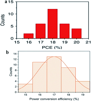 | ||
| Fig. 22 (a) Histogram of perovskite solar cell efficiencies based on MAPbI3:F4TCNQ films (with 0.03 wt% F4TCNQ). Reproduced by permission ref. 145, Copyright 2018 Springer Nature. (b) Histogram of 40 devices based on MA0.6FA0.38Cs0.02PbI2.975Br0.025: 5 mol% MACl perovskite. Reproduced by permission ref. 146, Copyright 2017 Wiley-VCH Verlag GmbH & Co. KGaA, Weinheim. | ||
Whitaker et al. demonstrated a perovskite device made by slot-die coating with a modified Coatema Easycoater slot-die coating station in ambient conditions.153 In this work, 5 different perovskite precursor concentrations with identical compositions (20% w/w, 23% w/w, 25% w/w, 30% w/w, and 40% w/w) were used for preparing the films. They observed that 23% w/w perovskite precursor concentration is optimum for this composition and device architecture. Fig. 23a shows an SEM image of slot-die coated MAPbI3 perovskite film and it was observed that the film consists of grains spreading over the film thickness. This is alluring for collecting charges across the film thickness. The top view scanning electron microscope images demonstrate that the film formed by slot-die coating is compact with least pinholes. In this perovskite thin film, the average grain size is estimated at approximate 1.5 mm. The power conversion efficiency with a slot-die coated layer was achieved up to 18% in reverse J–V sweep with the optimization of precursor concentration and coating speed. C. Zuo et al. developed a BADC (blowing-assisted drop-casting) technique to form MAPbI3 films in air.154 This BADC technique was then transferred to an in-house altered slot-die coater, which has a moving coating head with a connected gas blower. A compact and uniform MAPbI3 film was effectively formed utilizing the slot-die coating strategy (Fig. 23b). Perovskite solar cell was prepared in planar p–i–n structure using modified PEDOT:PSS as the HTL and efficiency was achieved up to 19.48% efficiency. The similar methodology was effectively translated to batch-to-batch slot-die coating and roll to roll processing, empowering the continuous production of MAPbI3 films with the improved morphology. Perovskite solar cells with a power conversion efficiency of 15.57% and 11.16% were accomplished by batch-processed slot-die-coating of perovskites on a glass substrate and the continuous R2R on PET substrate, separately. The developed BADC technique prompted to the acknowledgment of the best outcomes for the perovskite cells utilizing slot-die-coating and R2R processing. This work speaks to a noteworthy jump at advancing the R2R processing of PSCs. K. Hwang et al. reported the fabrication of PSCs by slot die coating strategy.155 All layers in the solar cell was fabricated through a scalable procedure using 3D printer based slot die coater. Using 3D printer x,y,z positions can be control with acceleration and speed control. Author used slot die coater with the gas-quenching process to produce pinhole-free PbI2 layer. Fig. 23c shows gas quenching process with slot die coating. The more uniform and dense film was formed in a gas quenched process comparison to naturally dried process. The naturally dried film had poor surface coverage. Very good uniform and a more dense film formed in the gas quenched process (Fig. 23d). Fig. 23g shows SEM image of slot-die coated MAI. Very small and round particles were formed at room temperature, which shows an incomplete perovskite layer. Accordingly, the conversion reaction was accelerated by heating the substrates and at 50 °C, cubic crystals were observed and complete conversion of the perovskite layer was obtained (Fig. 23h). At 70 °C temperature, cubic-shaped crystals size increases and it is around 1 μm (Fig. 23i) and more dense perovskite film forms. Burkitt et al. reported the fabrication of perovskite solar cell with four layers is coated by a slot-die coating method.156 It was observed that spin-coated films show insufficient surface coverage and many voids and slot-die coated films show better surface coverage and a more complete capping layer.
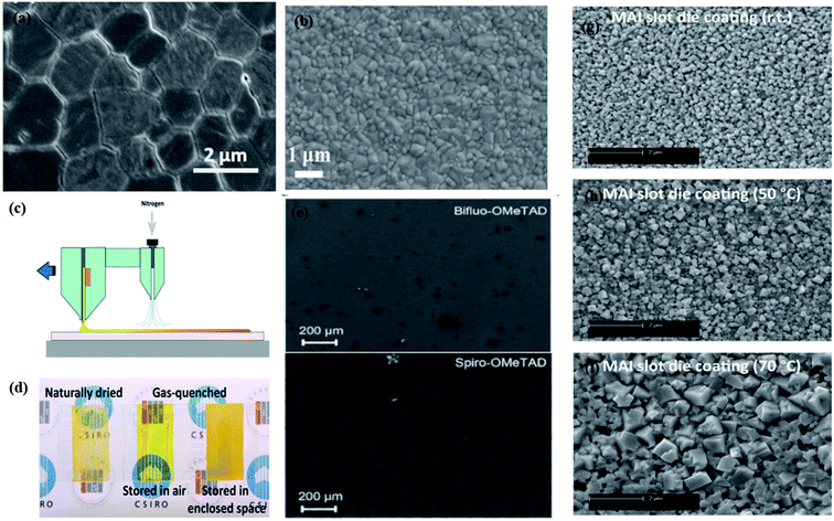 | ||
| Fig. 23 (a) Top view scanning electron microscope image of slot-die coated MAPbI3 perovskite thin film. Reproduced by permission ref. 153, Copyright 2018 Royal Society of Chemistry. (b) Scanning electron microscope image of slot-die coated CH3NH3PbI3 film. Reproduced by permission ref. 154, Copyright 2018 Elsevier Ltd. (c) Schematic diagram of slot-die coating with a gas-quenching process for the fabrication of pinhole-free PbI2 layer. (d) Images of PbI2 thin films formed by slot-die coating method under various coating conditions. Reproduced by permission ref. 155, Copyright 2015 Wiley-VCH Verlag GmbH & Co. KGaA, Weinheim. Scanning electron microscope images of slot-die coated (e) Bifluo-OMeTAD and (f) Spiro-OMeTAD on the underlying perovskite thin film. Reproduced by permission ref. 158, Copyright 2016 Elsevier Ltd. SEM images of the sequentially slot-die coated perovskite with various processing-temperatures PbI2 layers were slot-die coated and then converted to perovskite layer by a slot-die coating of MAI solution at room temperature (g), 50 °C (h), and 70 °C (i). Reproduced by permission ref. 155, Copyright 2015 Wiley-VCH Verlag GmbH & Co. KGaA, Weinheim. | ||
J. Ciro et al. reported flexible PSCs in ambient conditions produced by a slot-die coating method.157 Author observed that at 33 wt% precursor concentration and 80 °C temperature, best coverage percentage and surface roughness is obtained. T. Qin et al. reported a unique small molecule, 2,2′,7,7′-tetrakis(N,N-di-p-methoxyphenyl)amine-9,9′-bifluorenylidene (Bifluo-OMeTAD).158 The author has found this new HTM Bifluo-OMeTAD shows excellent film-forming properties and outperforms the Spiro-OMeTAD in the slot-die coated device. The enhanced film-forming properties of Bifluo-OMeTAD is accomplished via suppressing crystallization amid the slot-die-coating procedure. Additionally, with scanning electron microscopy (SEM) the surface of the Bifluo-OMeTAD sample presents a smooth surface with very few aggregating lumps (Fig. 23e), whereas Spiro-OMeTAD shows numerous clusters in 2–5 μm size (Fig. 23f).
The Bifluo-OMeTAD devices compared favorably to Spiro-OMeTAD devices with all performance parameters enhancing, yielding PCEs up to 14.7%, which is one of the most noteworthy (uncertified) reported values for slot-die coated perovskite solar cells. The good solubility and amorphous morphology also afford high quality thicker films. Y. Galagan et al. demonstrated with proven feasibility for roll to roll slot die coating of the electron transport layer and the perovskite layer on the 30 cm width flexible substrate in the ambient atmosphere.159 In this report 13.5% stabilized power conversion efficiency achieved. All the coatings of the electron transport layer and perovskite layer are performed in ambient conditions and industrially accepted solvents are used. Now slot-die coating technique is turned out to be high throughput and low-cost process for the large-scale manufacturing of PSCs. Be that as it may, building up a quick and effortless approach to manufacture large-area PSCs under the ambient condition is still needed.
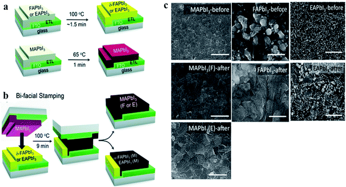 | ||
| Fig. 24 Schematic diagram of the stamping technique includes two steps. (a) Pre-annealing and (b) the bifacial stamping technique. (c) Plane-view scanning electron microscopy images of MAPbI3-before, MAPbI3(F)-after, MAPbI3(E)-after, FAPbI3-before, FAPbI3(M)-after, EAPbI3-before and EAPbI3-after. Scale bars are 1 μm. Reproduced by permission ref. 160, Copyright 2019 Royal Society of Chemistry. | ||
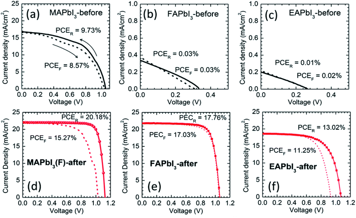 | ||
| Fig. 25 J–V curves of the best performing perovskite devices with forward and reverse scan. (a and d) MAPbI3, (b and e) FAPbI3 and (c and f) EAPbI3 before and after stamping, under AM1.5 one sun illumination. PCEF and PCER represent the efficiency values obtained from forward scanned and reverse scanned data respectively. Reproduced by permission ref. 160, Copyright 2019 Royal Society of Chemistry. | ||
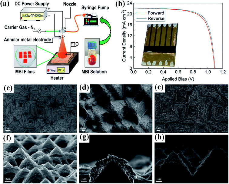 | ||
| Fig. 26 (a) Schematic illustration of spray coating process with the application of DC voltage used in the fabrication of lead free MA3Bi2I9 perovskite thin films. Reproduced by permission ref. 170, Copyright 2019 International Solar Energy Society. (b) J–V characteristics for the spraycast triple-cation PSC showing 17.8% efficiency in reverse scan. The device photograph is shown in inset. Reproduced by permission ref. 167, Copyright 2018 American Chemical Society. Top-view and cross-section SEM images of the spray-coated films onto the textured silicon bottom cell. (c and f) PbI2 NC ink, (d and g) MAPbI3 perovskite, and (e and h) CsFAMAPbI3−xBrx mixed perovskite films after spray conversion. Reproduced by permission ref. 169, Copyright 2020 Wiley-VCH Verlag GmbH & Co. KGaA, Weinheim. | ||
S. Sansoni et al. fabricated eco-friendly perovskite film on macroscale-textured surfaces by spray coating.169 In this work, CH3NH3PbI3 and CsFAMAPbI3−xBrx perovskite films were produced by sequential eco-friendly spray coating (SEF-SC) technique. The usage of toxic and dangerous solvents were avoided in this method. Fig. 26c–h shows the top-view and cross sectional scanning electron microscope images of perovskite films over the textured c-Si surfaces and all films shows the uniform coating with smaller crystal grains. T. Mohammad et al. fabricated the electric field assisted spray coated lead free methylammonium bismuth iodide perovskite thin film with different bias voltage from 0 to 1000 V.170Fig. 26a shows illustration of electric field assisted spray coating system. It was observed that morphology, homogeneity, crystallinity and surface roughness are influenced significantly by the electric field that is attributed to improve the atomization of spray droplets due to process of coulomb fission. In the absence of electric field loosely packed structure were observed and with the increase of electric field, packing density of grains was increased (Fig. 27c–e). Surface roughness was also decreased with the increased electric field.
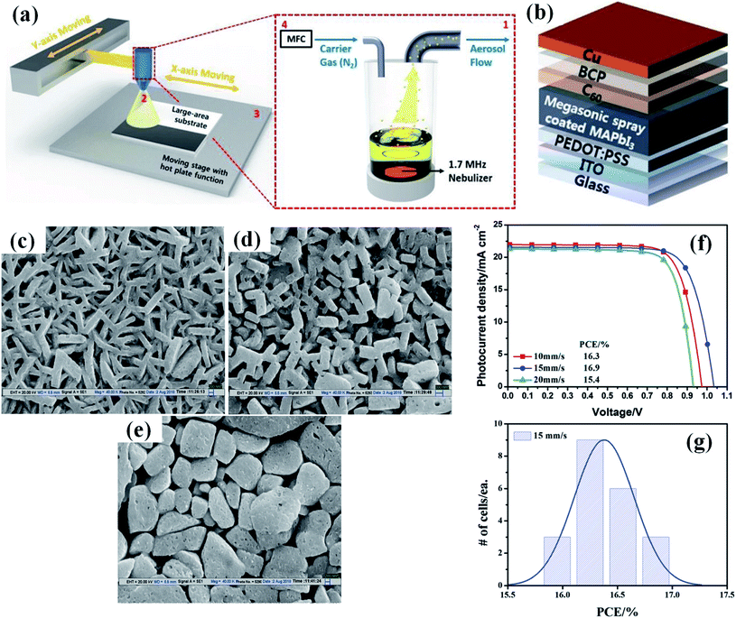 | ||
| Fig. 27 (a) Schematic illustration of the megasonic spray-coating method. (b) Device configuration of an inverted planar MAPbI3 PSC produced by the megasonic spray-coating method. Reproduced by permission ref. 173, Copyright 2018 Wiley-VCH Verlag GmbH & Co. KGaA, Weinheim. SEM image of lead free MA3Bi2I9 perovskite films at different bias during the deposition (c) 0 V (d) 500 V (e) 1000 V. Reproduced by permission ref. 170, Copyright 2019 International Solar Energy Society. (f) Current–voltage characteristics of the best performing devices with three different coating scan speeds. (g) Histogram of photovoltaic performance under 1 sun illumination of 21 samples with a coating scan speed of 15 mm s−1. Reproduced by permission ref. 173, Copyright 2018 Wiley-VCH Verlag GmbH & Co. KGaA, Weinheim. | ||
N. Kumar et al. used spray deposited nickel oxide films for fabrication of triple cation perovskite solar cells.171 In another report, X. Fan et al. used spray-coated monodispersed SnO2 microsphere films as scaffold layers for efficient mesoscopic perovskite solar cells with 17.08% efficiency.172 M. park et al. developed a megasonic spray-coating method for the fabrication of large area perovskite devices.173 The schematic representation of megasonic nebulizer spray system is shown in Fig. 27a which consists of four parts (i) the megasonic nebulizer source, (ii) the rectangular plastic nozzle, (iii) the motion stage and (iv) the mass flow controller. The scan speed is varied to 10, 15 and 20 mm s−1 for the fabrication of perovskite films and largest grain size was observed for 15 mm s−1 scan speed. Film thickness decreases linearly with the scan speed increasing. Device structure is shown in Fig. 27b and best efficiency was achieved 16.9% for the device made by 15 mm s−1 scan speed (Fig. 27f and g). Large grains in perovskite film lead to slow electronic recombination. This megasonic spray coating method is a unique technique for the polymer substrates, large area devices with low temperature and ambient conditions.
3. Summary and outlook
Among the current sustainable renewable energy technologies accessible nowadays, photovoltaic technologies are the foremost encouraging and quickest developing technologies that will provide a solution to the forthcoming energy crisis. Of all photovoltaic advancement, solution-processable perovskite materials have accomplished wonderful achievements in only a couple of years. They have been utilized in a horde of applications from solar cells to light-emitting devices and photodetectors. Notwithstanding, the noteworthy progression in such a small measure of time is remarkable and we may soon reach crystalline silicon and GaAs records towards the 29% imprint. Expecting that the field proceeds at the present rate of advancement, floated by the developing action, it is conceivable that a financially suitable option in contrast to silicon photovoltaics, or a material fit for improving silicon photovoltaics, will emerge throughout the following couple of years. Nevertheless, the most challenging aspect of PSCs is to grow a hydrophobic perovskite layer that can deliver a stable and high-performance perovskite device. In this review article, we have given the point of view toward the morphology optimization of the perovskite solar cell device and compositional development of halide perovskites to achieve highly efficient and long-term stable organic–inorganic hybrid perovskite solar cells. The control over the crystallinity and morphology of the perovskite was viewed as significant and exceptionally persuasive towards the overall performance of the solar cell. Here we discussed the impact of annealing conditions, precursor solution aging, precursor temperature, the addition of additives to the precursor solution, newly invented bifacial stamping method, PDL (post-device ligand) treatment, compositional engineering, interface engineering, solvent engineering, solvent vapor annealing, sequential deposition, doctor blading, slot-die coating and spray coating method on optimization of morphology and material properties of perovskites towards highly efficient and stable PSCs. The effect of additive, precursor temperature, aging, annealing, and concentration of MAI treatment on typical grain sizes in the films and the device performances were discussed. Hybrid perovskite films with larger grain sizes and fewer pinholes have been produced, from one perspective, either by producing additive-doped films or by forming chemical bonds with self-assembled monolayers or by adding a strongly coordinating solvent, improving interfacial contacts between electrode/electron transport materials (ETM) interface, ETM/perovskite interface, perovskite/hole transport materials (HTM) interface and HTM/electrode interface, thus reducing charge non-radiative recombination, simultaneously increasing the exciton diffusion length/lifetime. On the other hand, the crystallinity of hybrid perovskite layers can be increased under controlled temperature and humidity conditions, staying away from other chemical reactions and preventing the penetration of water, consequently improving the stability of hybrid perovskites. In spite of the quick advancement in the performance of hybrid perovskite solar cells, there are as yet a lot more opportunities for further improvement. Morphology engineering has the extraordinary potential to impressively increasing the efficiency and stability of hybrid perovskite solar cells. Nonetheless, the interaction mechanism between the hybrid perovskite and other interface layers still remains unclear and should be additionally investigated to facilitate the application of morphology optimization. Most of the techniques of morphology optimization have been limited to specific conditions during the fabrication of hybrid perovskite films. Concerning the following course in morphology optimization, film quality could be improved by either integrating these existing techniques with different functions or by investigating new technologies to achieve distinctive and goal-oriented morphology control. This has proceeded with the excitement in the field, in any case, some extra work needs are done to comprehend and improve further the photovoltaic parameters and long-term stability under operating conditions. There are absolutely difficulties staying in endeavoring to comprehend the role of ionic movement in long-term stability, and how to improve the already excellent photovoltaic parameters of perovskite solar cells. Future research ought to incorporate investigations on the impacts of defect type, defect density, and related photovoltaic effect mechanisms. Development of stable and efficient lead halide perovskite solar cells demands advance investigations to develop new materials and device structures to moderate the future power crisis. Notwithstanding experimental approaches, theoretical calculations still cannot be performed consistently in the area of morphology control, however, can make a noteworthy contribution to further advances in the design of morphological techniques. It is expected, however, that the PSC field will have additional years of exciting new findings, which will maintain the interest of both academia and industry.Conflicts of interest
There are no conflicts to declare.Acknowledgements
SS like to acknowledge Solar Energy Research Grant 2017 (DST SERI 0047) from Department of Science and Technology. M.I.D acknowledges the financial support from the Swiss National Science Foundation under the project number P300P2_174471.M.A.-J. thanks Cambridge Materials Limited, Wolfson College, University of Cambridge and EPSRC (grant no. EP/M005143/1) for their funding and technical support.References
- S. D. Stranks, G. E. Eperon, G. Grancini, C. Menelaou, M. J. Alcocer, T. Leijtens, L. M. Herz, A. Petrozza and H. J. Snaith, Science, 2013, 342, 341–344 CrossRef CAS PubMed.
- T. Baikie, Y. Fang, J. M. Kadro, M. Schreyer, F. Wei, S. G. Mhaisalkar, M. Graetzel and T. J. White, J. Mater. Chem. A, 2013, 1, 5628 RSC.
- D. Bi, A. M. El-Zohry, A. Hagfeldt and G. Boschloo, ACS Appl. Mater. Interfaces, 2014, 6, 18751–18757 CrossRef CAS PubMed.
- D. Bi, S.-J. Moon, L. Häggman, G. Boschloo, L. Yang, E. M. J. Johansson, M. K. Nazeeruddin, M. Grätzel and A. Hagfeldt, RSC Adv., 2013, 3, 18762 RSC.
- J. Burschka, N. Pellet, S. J. Moon, R. Humphry-Baker, P. Gao, M. K. Nazeeruddin and M. Gratzel, Nature, 2013, 499, 316–319 CrossRef CAS PubMed.
- Q. Chen, H. Zhou, Z. Hong, S. Luo, H. S. Duan, H. H. Wang, Y. Liu, G. Li and Y. Yang, J. Am. Chem. Soc., 2014, 136, 622–625 CrossRef CAS PubMed.
- N. J. Jeon, J. H. Noh, W. S. Yang, Y. C. Kim, S. Ryu, J. Seo and S. I. Seok, Nature, 2015, 517, 476–480 CrossRef CAS PubMed.
- H. J. Snaith, J. Phys. Chem. Lett., 2013, 4, 3623–3630 CrossRef CAS.
- M. A. Green, A. Ho-Baillie and H. J. Snaith, Nat. Photonics, 2014, 8, 506–514 CrossRef CAS.
- P. Schouwink, M. B. Ley, A. Tissot, H. Hagemann, T. R. Jensen, L. Smrcok and R. Cerny, Nat. Commun., 2014, 5, 5706 CrossRef CAS PubMed.
- J. P. Correa-Baena, A. Abate, M. Saliba, W. Tress, T. J. Jacobsson, M. Gratzel and A. Hagfeldt, Energy Environ. Sci., 2017, 10, 710–727 RSC.
- A. Dubey, N. Adhikari, S. Mabrouk, F. Wu, K. Chen, S. Yang and Q. Qiao, J. Mater. Chem. A, 2018, 6, 2406–2431 RSC.
- H.-S. Kim, S. H. Im and N.-G. Park, J. Phys. Chem. C, 2014, 118, 5615–5625 CrossRef CAS.
- C. Li, X. Lu, W. Ding, L. Feng, Y. Gao and Z. Guo, Acta Crystallogr., Sect. B: Struct. Sci., 2008, 64, 702–707 CrossRef CAS PubMed.
- A. B. Djurišić, F. Z. Liu, H. W. Tam, M. K. Wong, A. Ng, C. Surya, W. Chen and Z. B. He, Prog. Quantum Electron., 2017, 53, 1–37 CrossRef.
- W.-J. Yin, J.-H. Yang, J. Kang, Y. Yan and S.-H. Wei, J. Mater. Chem. A, 2015, 3, 8926–8942 RSC.
- M. Stolterfoht, M. Grischek, P. Caprioglio, C. M. Wolff, E. Gutierrez-Partida, F. Pena-Camargo, D. Rothhardt, S. Zhang, M. Raoufi, J. Wolansky, M. Abdi-Jalebi, S. D. Stranks, S. Albrecht, T. Kirchartz and D. Neher, Adv. Mater., 2020 DOI:10.1002/adma.202000080.
- J. Lu, X. Lin, X. Jiao, T. Gengenbach, A. D. Scully, L. Jiang, B. Tan, J. Sun, B. Li, N. Pai, U. Bach, A. N. Simonov and Y.-B. Cheng, Energy Environ. Sci., 2018, 11, 1880–1889 RSC.
- Z. Wu, Z. Liu, Z. Hu, Z. Hawash, L. Qiu, Y. Jiang, L. K. Ono and Y. Qi, Adv. Mater., 2019, 31, e1804284 CrossRef PubMed.
- J. A. Christians, P. Schulz, J. S. Tinkham, T. H. Schloemer, S. P. Harvey, B. J. T. de Villers, A. Sellinger, J. J. Berry and J. M. Luther, Nat. Energy, 2018, 3, 68–74 CrossRef CAS.
- T. Salim, S. Sun, Y. Abe, A. Krishna, A. C. Grimsdale and Y. M. Lam, J. Mater. Chem. A, 2015, 3, 8943–8969 RSC.
- M. Feng, S. You, N. Cheng and J. Du, Electrochim. Acta, 2019, 293, 356–363 CrossRef CAS.
- Z. Xiao, Q. Dong, C. Bi, Y. Shao, Y. Yuan and J. Huang, Adv. Mater., 2014, 26, 6503–6509 CrossRef CAS PubMed.
- M. Xiao, F. Huang, W. Huang, Y. Dkhissi, Y. Zhu, J. Etheridge, A. Gray-Weale, U. Bach, Y. B. Cheng and L. Spiccia, Angew. Chem., Int. Ed., 2014, 53, 9898–9903 CrossRef CAS PubMed.
- M. S. Jamal, M. S. Bashar, A. K. M. Hasan, Z. A. Almutairi, H. F. Alharbi, N. H. Alharthi, M. R. Karim, H. Misran, N. Amin, K. Bin Sopian and M. Akhtaruzzaman, Renewable Sustainable Energy Rev., 2018, 98, 469–488 CrossRef CAS.
- Y. Li, L. Ji, R. Liu, C. Zhang, C. H. Mak, X. Zou, H.-H. Shen, S.-Y. Leu and H.-Y. Hsu, J. Mater. Chem. A, 2018, 6, 12842–12875 RSC.
- M. Abd Mutalib, F. Aziz, A. F. Ismail, W. N. Wan Salleh, N. Yusof, J. Jaafar, T. Soga, M. Z. Sahdan and N. Ahmad Ludin, Appl. Mater. Today, 2018, 13, 69–82 CrossRef.
- H. S. Kim, A. Hagfeldt and N. G. Park, Chem. Commun., 2019, 55, 1192–1200 RSC.
- W. Chen, Y. Wu, Y. Yue, J. Liu, W. Zhang, X. Yang, H. Chen, E. Bi, I. Ashraful, M. Gratzel and L. Han, Science, 2015, 350, 944–948 CrossRef CAS PubMed.
- A. Priyadarshi, L. J. Haur, P. Murray, D. Fu, S. Kulkarni, G. Xing, T. C. Sum, N. Mathews and S. G. Mhaisalkar, Energy Environ. Sci., 2016, 9, 3687–3692 RSC.
- Y. Deng, E. Peng, Y. Shao, Z. Xiao, Q. Dong and J. Huang, Energy Environ. Sci., 2015, 8, 1544–1550 RSC.
- A. Raghav, S. Singh, S. K. Sharma, D. Kabra, M. Bag and S. Satapathi, Nano-Struct. Nano-Objects, 2017, 12, 106–112 CrossRef CAS.
- Z. Yang, S. Zhang, L. Li and W. Chen, J. Materiomics, 2017, 3, 231–244 CrossRef.
- S. D. Stranks, P. K. Nayak, W. Zhang, T. Stergiopoulos and H. J. Snaith, Angew. Chem., Int. Ed., 2015, 54, 3240–3248 CrossRef CAS PubMed.
- C. Tao, S. Neutzner, L. Colella, S. Marras, A. R. Srimath Kandada, M. Gandini, M. D. Bastiani, G. Pace, L. Manna, M. Caironi, C. Bertarelli and A. Petrozza, Energy Environ. Sci., 2015, 8, 2365–2370 RSC.
- Z. K. Wang, M. Li, Y. G. Yang, Y. Hu, H. Ma, X. Y. Gao and L. S. Liao, Adv. Mater., 2016, 28, 6695–6703 CrossRef CAS PubMed.
- C. Wehrenfennig, G. E. Eperon, M. B. Johnston, H. J. Snaith and L. M. Herz, Adv. Mater., 2014, 26, 1584–1589 CrossRef CAS PubMed.
- X. Zhang, L. Li, Z. Sun and J. Luo, Chem. Soc. Rev., 2019, 48, 517–539 RSC.
- Q. Guo, F. Yuan, B. Zhang, S. Zhou, J. Zhang, Y. Bai, L. Fan, T. Hayat, A. Alsaedi and Z. Tan, Nanoscale, 2018, 11, 115–124 RSC.
- L.-C. Chen, C.-C. Chen, J.-C. Chen and C.-G. Wu, Sol. Energy, 2015, 122, 1047–1051 CrossRef CAS.
- A. Dualeh, N. Tétreault, T. Moehl, P. Gao, M. K. Nazeeruddin and M. Grätzel, Adv. Funct. Mater., 2014, 24, 3250–3258 CrossRef CAS.
- G. E. Eperon, V. M. Burlakov, P. Docampo, A. Goriely and H. J. Snaith, Adv. Funct. Mater., 2014, 24, 151–157 CrossRef CAS.
- L. Huang, Z. Hu, J. Xu, K. Zhang, J. Zhang and Y. Zhu, Sol. Energy Mater. Sol. Cells, 2015, 141, 377–382 CrossRef CAS.
- D. P. Nenon, J. A. Christians, L. M. Wheeler, J. L. Blackburn, E. M. Sanehira, B. Dou, M. L. Olsen, K. Zhu, J. J. Berry and J. M. Luther, Energy Environ. Sci., 2016, 9, 2072–2082 RSC.
- J. J. van Franeker, K. H. Hendriks, B. J. Bruijnaers, M. W. G. M. Verhoeven, M. M. Wienk and R. A. J. Janssen, Adv. Energy Mater., 2017, 7, 1601822 CrossRef.
- A. Dualeh, N. Tetreault, T. Moehl, P. Gao, M. K. Nazeeruddin and M. Gratzel, Adv. Funct. Mater., 2014, 24, 3250–3258 CrossRef CAS.
- W. Y. Nie, H. H. Tsai, R. Asadpour, J. C. Blancon, A. J. Neukirch, G. Gupta, J. J. Crochet, M. Chhowalla, S. Tretiak, M. A. Alam, H. L. Wang and A. D. Mohite, Science, 2015, 347, 522–525 CrossRef CAS PubMed.
- Y. H. Deng, Q. Wang, Y. B. Yuan and J. S. Huang, Mater. Horiz., 2015, 2, 578–583 RSC.
- C. Wu, Q. Zhang, Y. Liu, W. Luo, X. Guo, Z. Huang, H. Ting, W. Sun, X. Zhong, S. Wei, S. Wang, Z. Chen and L. Xiao, Adv. Sci., 2018, 5, 1700759 CrossRef PubMed.
- H. Tsai, W. Nie, Y.-H. Lin, J. C. Blancon, S. Tretiak, J. Even, G. Gupta, P. M. Ajayan and A. D. Mohite, Adv. Energy Mater., 2017, 7, 1602159 CrossRef.
- P. Boonmongkolras, D. Kim, E. M. Alhabshi, I. Gereige and B. Shin, RSC Adv., 2018, 8, 21551–21557 RSC.
- B. J. Dou, L. M. Wheeler, J. A. Christians, D. T. Moore, S. P. Harvey, J. J. Berry, F. S. Barnes, S. E. Shaheen and M. F. A. M. van Hest, ACS Energy Lett., 2018, 3, 979–985 CrossRef CAS.
- G. Namkoong, A. A. Mamun, T. T. Ava, K. Zhang and H. Baumgart, Org. Electron., 2017, 42, 228–233 CrossRef CAS.
- D. Bi, X. Li, J. V. Milic, D. J. Kubicki, N. Pellet, J. Luo, T. LaGrange, P. Mettraux, L. Emsley, S. M. Zakeeruddin and M. Gratzel, Nat. Commun., 2018, 9, 4482 CrossRef PubMed.
- X.-X. Gao, D.-J. Xue, D. Gao, Q. Han, Q.-Q. Ge, J.-Y. Ma, J. Ding, W. Zhang, B. Zhang, Y. Feng, G. Yu and J.-S. Hu, Sol. RRL, 2019, 3, 1800232 CrossRef.
- S. N. Habisreutinger, T. Leijtens, G. E. Eperon, S. D. Stranks, R. J. Nicholas and H. J. Snaith, Nano Lett., 2014, 14, 5561–5568 CrossRef CAS PubMed.
- T. Leijtens, T. Giovenzana, S. N. Habisreutinger, J. S. Tinkham, N. K. Noel, B. A. Kamino, G. Sadoughi, A. Sellinger and H. J. Snaith, ACS Appl. Mater. Interfaces, 2016, 8, 5981–5989 CrossRef CAS PubMed.
- C. Liu, W. Ding, X. Zhou, J. Gao, C. Cheng, X. Zhao and B. Xu, J. Phys. Chem. C, 2017, 121, 6546–6553 CrossRef CAS.
- J. H. Noh, S. H. Im, J. H. Heo, T. N. Mandal and S. I. Seok, Nano Lett., 2013, 13, 1764–1769 CrossRef CAS PubMed.
- J. Yin, J. Cao, X. He, S. Yuan, S. Sun, J. Li, N. Zheng and L. Lin, J. Mater. Chem. A, 2015, 3, 16860–16866 RSC.
- J. Zhao, B. Cai, Z. Luo, Y. Dong, Y. Zhang, H. Xu, B. Hong, Y. Yang, L. Li, W. Zhang and C. Gao, Sci. Rep., 2016, 6, 21976 CrossRef CAS PubMed.
- X. Li, M. I. Dar, C. Yi, J. Luo, M. Tschumi, S. M. Zakeeruddin, M. K. Nazeeruddin, H. Han and M. Gratzel, Nat. Chem., 2015, 7, 703–711 CrossRef CAS PubMed.
- M. Saliba, T. Matsui, K. Domanski, J. Y. Seo, A. Ummadisingu, S. M. Zakeeruddin, J. P. Correa-Baena, W. R. Tress, A. Abate, A. Hagfeldt and M. Gratzel, Science, 2016, 354, 206–209 CrossRef CAS PubMed.
- R. Uchida, S. Binet, N. Arora, G. Jacopin, M. H. Alotaibi, A. Taubert, S. M. Zakeeruddin, M. I. Dar and M. Graetzel, Small, 2018, 14, e1802033 CrossRef PubMed.
- A. Albadri, P. Yadav, M. Alotaibi, N. Arora, A. Alyamani, H. Albrithen, M. I. Dar, S. M. Zakeeruddin and M. Gratzel, J. Phys. Chem. C, 2017, 121, 24903–24908 CrossRef CAS.
- P. Yadav, M. I. Dar, N. Arora, E. A. Alharbi, F. Giordano, S. M. Zakeeruddin and M. Gratzel, Adv. Mater., 2017, 29, 1701077 CrossRef PubMed.
- E. A. Alharbi, M. I. Dar, N. Arora, M. H. Alotaibi, Y. A. Alzhrani, P. Yadav, W. Tress, A. Alyamani, A. Albadri, S. M. Zakeeruddin and M. Grätzel, Research, 2019, 2019, 1–9 CrossRef PubMed.
- M. H. Alotaibi, Y. A. Alzahrani, N. Arora, A. Alyamani, A. Albadri, H. Albrithen, I. H. Al-Lehyani, S. M. Alenzi, A. Z. Alanzi, F. S. Alghamdi, S. M. Zakeeruddin, S. Meloni, M. I. Dar and M. Graetzel, Sol. RRL, 2019, 1900234, DOI:10.1002/solr.201900234.
- M. Abdi-Jalebi, M. I. Dar, A. Sadhanala, S. P. Senanayak, M. Franckevičius, N. Arora, Y. Hu, M. K. Nazeeruddin, S. M. Zakeeruddin, M. Grätzel and R. H. Friend, Adv. Energy Mater., 2016, 6, 1502472 CrossRef.
- H. Zheng, D. Liu, Y. Wang, Y. Yang, H. Li, T. Zhang, H. Chen, L. Ji, Z. Chen and S. Li, Chem. Eng. J., 2020, 389, 124266 CrossRef CAS.
- J. Jiang, X. Fang, Y. Xu, X. Jia, Y. Chen, Y. Chen, H. Hu, N. Yuan and J. Ding, ChemSusChem, 2020, 13, 412–418 CrossRef CAS PubMed.
- H. W. Lei, P. Dai, X. R. Wang, Z. W. Pan, Y. X. Guo, H. Shen, J. J. Chen, J. Xie, B. Zhang, S. Zhang and Z. J. Tan, Adv. Mater. Interfaces, 2020, 7, 1901716 CrossRef CAS.
- Z. Ma, Z. Xiao, W. Y. Zhou, L. F. Jin, D. J. Huang, H. F. Jiang, T. Yang, Y. C. Liu and Y. L. Huang, J. Alloys Compd., 2020, 822, 153539 CrossRef CAS.
- J. Zhu, B. He, Z. Gong, Y. Ding, W. Zhang, X. Li, Z. Zong, H. Chen and Q. Tang, ChemSusChem, 2020, 13, 1834–1843 CrossRef CAS PubMed.
- D. Xin, S. Tie, X. Zheng, J. Zhu and W.-H. Zhang, J. Energy Chem., 2020, 46, 173–177 CrossRef.
- M. A. Afroz, R. K. Gupta, R. Garai, M. Hossain, S. P. Tripathi and P. K. Iyer, Org. Electron., 2019, 74, 172–178 CrossRef CAS.
- L. Su, Y. Xiao, L. Lu, G. Han and M. Zhu, Org. Electron., 2020, 77, 105519 CrossRef CAS.
- F. Zhang and K. Zhu, Adv. Energy Mater., 2019, 1902579, DOI:10.1002/aenm.201902579.
- J. W. Lee, H. S. Kim and N. G. Park, Acc. Chem. Res., 2016, 49, 311–319 CrossRef CAS PubMed.
- J. Luo, J. Xia, H. Yang, H. A. Malik, F. Han, H. Shu, X. Yao, Z. Wan and C. Jia, Nano Energy, 2020, 70, 104509 CrossRef CAS.
- S. Satapathi, F. Yan, R. Anandakathir, K. Yang, L. Li, R. Mosurkal, L. A. Samuelson and Jayant Kumar, J. Macromol. Sci. A, 2010, 47, 1180–1183 CrossRef CAS.
- J. Wang, J. Zhang, Y. Zhou, H. Liu, Q. Xue, X. Li, C. C. Chueh, H. L. Yip, Z. Zhu and A. K. Y. Jen, Nat. Commun., 2020, 11, 177 CrossRef CAS PubMed.
- S. G. Ko, G. I. Ryu, B. Kim, G. J. Cha, J. H. Ri, G. S. Sonu and U. C. Kim, Sol. Energy Mater. Sol. Cells, 2019, 196, 105–110 CrossRef CAS.
- Y. Y. Zhao, Y. D. Wang, J. L. Duan, X. Y. Yang and Q. W. Tang, J. Mater. Chem. A, 2019, 7, 6877–6882 RSC.
- F. Zhang, D. Bi, N. Pellet, C. Xiao, Z. Li, J. J. Berry, S. M. Zakeeruddin, K. Zhu and M. Grätzel, Energy Environ. Sci., 2018, 11, 3480–3490 RSC.
- H. Zhang, X. Ren, X. Chen, J. Mao, J. Cheng, Y. Zhao, Y. Liu, J. Milic, W.-J. Yin, M. Grätzel and W. C. H. Choy, Energy Environ. Sci., 2018, 11, 2253–2262 RSC.
- J. C. Dahl, W. T. Osowiecki, Y. Cai, J. K. Swabeck, Y. Bekenstein, M. Asta, E. M. Chan and A. P. Alivisatos, Chem. Mater., 2019, 31, 3134–3143 CrossRef CAS.
- T. Singh and T. Miyasaka, Adv. Energy Mater., 2018, 8, 1700677 CrossRef.
- M. Saliba, T. Matsui, J. Y. Seo, K. Domanski, J. P. Correa-Baena, M. K. Nazeeruddin, S. M. Zakeeruddin, W. Tress, A. Abate, A. Hagfeldt and M. Gratzel, Energy Environ. Sci., 2016, 9, 1989–1997 RSC.
- T. Matsui, T. Yamamoto, T. Nishihara, R. Morisawa, T. Yokoyama, T. Sekiguchi and T. Negami, Adv. Mater., 2019, 31, e1806823 CrossRef PubMed.
- M. Abdi-Jalebi, Z. Andaji-Garmaroudi, S. Cacovich, C. Stavrakas, B. Philippe, J. M. Richter, M. Alsari, E. P. Booker, E. M. Hutter, A. J. Pearson, S. Lilliu, T. J. Savenije, H. Rensmo, G. Divitini, C. Ducati, R. H. Friend and S. D. Stranks, Nature, 2018, 555, 497–501 CrossRef CAS PubMed.
- M. Abdi-Jalebi, Z. Andaji-Garmaroudi, A. J. Pearson, G. Divitini, S. Cacovich, B. Philippe, H. Rensmo, C. Ducati, R. H. Friend and S. D. Stranks, ACS Energy Lett., 2018, 3, 2671–2678 CrossRef CAS PubMed.
- P. O'Keeffe, D. Catone, A. Paladini, F. Toschi, S. Turchini, L. Avaldi, F. Martelli, A. Agresti, S. Pescetelli, A. E. Del Rio Castillo, F. Bonaccorso and A. Di Carlo, Nano Lett., 2019, 19, 684–691 CrossRef PubMed.
- M. M. Tavakoli, M. Saliba, P. Yadav, P. Holzhey, A. Hagfeldt, S. M. Zakeeruddin and M. Grätzel, Adv. Energy Mater., 2019, 9, 1802646 CrossRef.
- M. M. Tavakoli, R. Tavakoli, P. Yadav and J. Kong, J. Mater. Chem. A, 2019, 7, 679–686 RSC.
- B. Li, Z. Chen, H. Yao, X. Guan, Z. Yu, F. Halis Isikgor, H. Coskun, Q. H. Xu and J. Ouyang, Nanoscale, 2019, 11, 3216–3221 RSC.
- S. S. Mali, J. V. Patil, H. Kim, R. Luque and C. K. Hong, Mater. Today, 2019, 26, 8–18 CrossRef CAS.
- Y. Jiang, M. Remeika, Z. Hu, E. J. Juarez-Perez, L. Qiu, Z. Liu, T. Kim, L. K. Ono, D. Y. Son, Z. Hawash, M. R. Leyden, Z. Wu, L. Meng, J. Hu and Y. Qi, Adv. Energy Mater., 2019, 9, 1803047 CrossRef.
- M. M. Tavakoli, R. Tavakoli, P. Yadav and J. Kong, J. Mater. Chem. A, 2019, 7, 679–686 RSC.
- M. M. Tavakoli, M. Saliba, P. Yadav, P. Holzhey, A. Hagfeldt, S. M. Zakeeruddin and M. Gratzel, Adv. Energy Mater., 2019, 9, 1802646 CrossRef.
- M. Abdi-Jalebi, M. Ibrahim Dar, S. P. Senanayak, A. Sadhanala, Z. Andaji-Garmaroudi, L. M. Pazos-Outon, J. M. Richter, A. J. Pearson, H. Sirringhaus, M. Gratzel and R. H. Friend, Sci. Adv., 2019, 5, eaav2012 CrossRef CAS PubMed.
- J. F. Lu, X. F. Lin, X. C. Jiao, T. Gengenbach, A. D. Scully, L. C. Jiang, B. Tan, J. S. Sun, B. Li, N. Pai, U. Bach, A. N. Simonov and Y. B. Cheng, Energy Environ. Sci., 2018, 11, 1880–1889 RSC.
- N. Arora, M. I. Dar, A. Hinderhofer, N. Pellet, F. Schreiber, S. M. Zakeeruddin and M. Gratzel, Science, 2017, 358, 768–771 CrossRef CAS PubMed.
- W. N. Liu, J. J. Zheng, M. H. Shang, Z. Fang, K. C. Chou, W. Y. Yang, X. M. Hou and T. Wu, J. Mater. Chem. A, 2019, 7, 10912–10917 RSC.
- K.-M. Lee, C.-J. Lin, B.-Y. Liou, S.-M. Yu, C.-C. Hsu and V. Suryanarayanan, Org. Electron., 2019, 65, 266–274 CrossRef CAS.
- J. Liu, N. Li, J. Jia, J. Dong, Z. Qiu, S. Iqbal and B. Cao, Sol. Energy, 2019, 181, 285–292 CrossRef CAS.
- D. Xin, Z. Wang, M. Zhang, X. Zheng, Y. Qin, J. Zhu and W.-H. Zhang, ACS Sustainable Chem. Eng., 2019, 7, 4343–4350 CrossRef CAS.
- Z. Nie, J. Yin, H. Zhou, N. Chai, B. Chen, Y. Zhang, K. Qu, G. Shen, H. Ma, Y. Li, J. Zhao and X. Zhang, ACS Appl. Mater. Interfaces, 2016, 8, 28187–28193 CrossRef CAS PubMed.
- A. Raghav, S. Singh, S. K. Sharma, D. Kabra, M. Bag and S. Satapathi, Nano-Struct. Nano-Objects, 2017, 12, 106–112 CrossRef CAS.
- M. Schreier, L. Curvat, F. Giordano, L. Steier, A. Abate, S. M. Zakeeruddin, J. Luo, M. T. Mayer and M. Gratzel, Nat. Commun., 2015, 6, 7326 CrossRef CAS PubMed.
- M. I. Dar, A. Hinderhofer, G. Jacopin, V. Belova, N. Arora, S. M. Zakeeruddin, F. Schreiber and M. Gratzel, Adv. Funct. Mater., 2017, 27, 1701433 CrossRef.
- N. Arora, M. I. Dar, M. Hezam, W. Tress, G. Jacopin, T. Moehl, P. Gao, A. S. Aldwayyan, B. Deveaud, M. Gratzel and M. K. Nazeeruddin, Adv. Funct. Mater., 2016, 26, 2846–2854 CrossRef CAS.
- N. Arora, M. I. Dar, M. Abdi-Jalebi, F. Giordano, N. Pellet, G. Jacopin, R. H. Friend, S. M. Zakeeruddin and M. Gratzel, Nano Lett., 2016, 16, 7155–7162 CrossRef CAS PubMed.
- M. I. Dar, N. Arora, C. Steck, A. Mishra, M. H. Alotaibi, P. Bauerle, S. M. Zakeeruddin and M. Gratzel, Eur. J. Inorg. Chem., 2018, 4573–4578 CrossRef CAS.
- G. Liu, Z. Liu, F. Zeng, X. Wang, S. Li and X. Xie, Chem. Phys. Lett., 2020, 743, 137186 CrossRef CAS.
- J. Liu, C. Gao, X. He, Q. Ye, L. Ouyang, D. Zhuang, C. Liao, J. Mei and W. Lau, ACS Appl. Mater. Interfaces, 2015, 7, 24008–24015 CrossRef CAS PubMed.
- H. Xiong, G. DeLuca, Y. Rui, Y. Li, E. Reichmanis, Q. Zhang and H. Wang, Sol. Energy Mater. Sol. Cells, 2017, 166, 167–175 CrossRef CAS.
- F. Zhang, J. Song, L. Zhang, F. Niu, Y. Hao, P. Zeng, H. Niu, J. Huang and J. Lian, J. Mater. Chem. A, 2016, 4, 8554–8561 RSC.
- T. Liu, Q. Hu, J. Wu, K. Chen, L. Zhao, F. Liu, C. Wang, H. Lu, S. Jia, T. Russell, R. Zhu and Q. Gong, Adv. Energy Mater., 2016, 6, 1501890 CrossRef.
- S. Kim, T. Chung, S. Bae, S.-W. Lee, K. D. Lee, H. Kim, S. Lee, Y. Kang, H.-S. Lee and D. Kim, Org. Electron., 2017, 41, 266–273 CrossRef CAS.
- H. Mehdi, A. Mhamdi, R. Hannachi and A. Bouazizi, RSC Adv., 2019, 9, 12906–12912 RSC.
- L. Zheng, Y. Ma, S. Chu, S. Wang, B. Qu, L. Xiao, Z. Chen, Q. Gong, Z. Wu and X. Hou, Nanoscale, 2014, 6, 8171–8176 RSC.
- J. H. Im, I. H. Jang, N. Pellet, M. Gratzel and N. G. Park, Nat. Nanotechnol., 2014, 9, 927–932 CrossRef CAS PubMed.
- S. I. Seok, M. Gratzel and N. G. Park, Small, 2018, 14, e1704177 CrossRef PubMed.
- Q. Jiang, L. Zhang, H. Wang, X. Yang, J. Meng, H. Liu, Z. Yin, J. Wu, X. Zhang and J. You, Nat. Energy, 2016, 2, 16177 CrossRef.
- S. Kim, T. Chung, S. Bae, S. W. Lee, K. D. Lee, H. Kim, S. Lee, Y. Kang, H. S. Lee and D. Kim, Org. Electron., 2017, 41, 266–273 CrossRef CAS.
- M. I. Dar, N. Arora, P. Gao, S. Ahmad, M. Gratzel and M. K. Nazeeruddin, Nano Lett., 2014, 14, 6991–6996 CrossRef CAS PubMed.
- M. I. Dar, M. Abdi-Jalebi, N. Arora, M. Gratzel and M. K. Nazeeruddin, Adv. Energy Mater., 2016, 6, 1501358 CrossRef.
- M. Ibrahim Dar, M. Abdi-Jalebi, N. Arora, T. Moehl, M. Gratzel and M. K. Nazeeruddin, Adv. Mater., 2015, 27, 7221–7228 CrossRef CAS PubMed.
- Y. Y. Kim, E. Y. Park, T. Y. Yang, J. H. Noh, T. J. Shin, N. J. Jeon and J. Seo, J. Mater. Chem. A, 2018, 6, 12447–12454 RSC.
- C. Yi, X. Li, J. Luo, S. M. Zakeeruddin and M. Gratzel, Adv. Mater., 2016, 28, 2964–2970 CrossRef CAS PubMed.
- Q. Li, Y. Zhao, R. Fu, W. Zhou, Y. Zhao, X. Liu, D. Yu and Q. Zhao, Adv. Mater., 2018, e1803095, DOI:10.1002/adma.201803095.
- Y. H. Deng, E. Peng, Y. C. Shao, Z. G. Xiao, Q. F. Dong and J. S. Huang, Energy Environ. Sci., 2015, 8, 1544–1550 RSC.
- S. Razza, F. Di Giacomo, F. Matteocci, L. Cinà, A. L. Palma, S. Casaluci, P. Cameron, A. D'Epifanio, S. Licoccia, A. Reale, T. M. Brown and A. Di Carlo, J. Power Sources, 2015, 277, 286–291 CrossRef CAS.
- J. L. Yang, D. Vak, N. Clark, J. Subbiah, W. W. H. Wong, D. J. Jones, S. E. Watkins and G. Wilson, Sol. Energy Mater. Sol. Cells, 2013, 109, 47–55 CrossRef CAS.
- Z. B. Yang, C. C. Chueh, F. Zuo, J. H. Kim, P. W. Liang and A. K. Y. Jen, Adv. Energy Mater., 2015, 5, 1500328 CrossRef.
- F. Huang, M. Li, P. Siffalovic, G. Cao and J. Tian, Energy Environ. Sci., 2019, 12, 518–549 RSC.
- D. Wang, J. Zheng, X. Wang, J. Gao, W. Kong, C. Cheng and B. Xu, J. Energy Chem., 2019, 38, 207–213 CrossRef.
- M. Ye, X. Hong, F. Zhang and X. Liu, J. Mater. Chem. A, 2016, 4, 6755–6771 RSC.
- J. H. Kim, S. T. Williams, N. Cho, C. C. Chueh and A. K. Y. Jen, Adv. Energy Mater., 2015, 5, 1401229 CrossRef.
- H. Wu, C. J. Zhang, K. X. Ding, L. J. Wang, Y. L. Gao and J. L. Yang, Org. Electron., 2017, 45, 302–307 CrossRef CAS.
- S. C. Tong, H. Wu, C. J. Zhang, S. G. Li, C. H. Wang, J. Q. Shen, S. Xiao, J. He, J. L. Yang, J. Sun and Y. L. Gao, Org. Electron., 2017, 49, 347–354 CrossRef CAS.
- Y. H. Deng, Q. F. Dong, C. Bi, Y. B. Yuan and J. S. Huang, Adv. Energy Mater., 2016, 6, 1600372 CrossRef.
- S. G. Li, S. C. Tong, J. L. Yang, H. Y. Xia, C. J. Zhang, C. Zhang, J. Q. Shen, S. Xiao, J. He, Y. L. Gao, B. C. Yang and J. Q. Meng, Org. Electron., 2017, 47, 102–107 CrossRef CAS.
- W. Q. Wu, Q. Wang, Y. Fang, Y. Shao, S. Tang, Y. Deng, H. Lu, Y. Liu, T. Li, Z. Yang, A. Gruverman and J. Huang, Nat. Commun., 2018, 9, 1625 CrossRef PubMed.
- S. Tang, Y. H. Deng, X. P. Zheng, Y. Bai, Y. J. Fang, Q. F. Dong, H. T. Wei and J. S. Huang, Adv. Energy Mater., 2017, 7, 1700302 CrossRef.
- T. M. Schmidt, T. T. Larsen-Olsen, J. E. Carle, D. Angmo and F. C. Krebs, Adv. Energy Mater., 2015, 5, 1500569 CrossRef.
- B. Dou, J. B. Whitaker, K. Bruening, D. T. Moore, L. M. Wheeler, J. Ryter, N. J. Breslin, J. J. Berry, S. M. Garner, F. S. Barnes, S. E. Shaheen, C. J. Tassone, K. Zhu and M. F. A. M. van Hest, ACS Energy Lett., 2018, 3, 2558–2565 CrossRef CAS.
- Y. C. Huang, C. F. Li, Z. H. Huang, P. H. Liu and C. S. Tsao, Sol. Energy, 2019, 177, 255–261 CrossRef CAS.
- M. Remeika, L. K. Ono, M. Maeda, Z. H. Hu and Y. B. Qi, Org. Electron., 2018, 54, 72–79 CrossRef CAS.
- Y.-C. Huang, C.-F. Li, Z.-H. Huang, P.-H. Liu and C.-S. Tsao, Sol. Energy, 2019, 177, 255–261 CrossRef CAS.
- J. E. Kim, S. S. Kim, C. Zuo, M. Gao, D. Vak and D. Y. Kim, Adv. Funct. Mater., 2019, 1809194, DOI:10.1002/adfm.201809194.
- J. B. Whitaker, D. H. Kim, B. W. Larson, F. Zhang, J. J. Berry, M. F. A. M. van Hest and K. Zhu, Sustainable Energy Fuels, 2018, 2, 2442–2449 RSC.
- C. T. Zuo, D. Vak, D. Angmo, L. M. Ding and M. Gao, Nano Energy, 2018, 46, 185–192 CrossRef CAS.
- K. Hwang, Y. S. Jung, Y. J. Heo, F. H. Scholes, S. E. Watkins, J. Subbiah, D. J. Jones, D. Y. Kim and D. Vak, Adv. Mater., 2015, 27, 1241–1247 CrossRef CAS PubMed.
- D. Burkitt, J. Searle and T. Watson, R. Soc. Open Sci., 2018, 5, 172158 CrossRef PubMed.
- J. Ciro, M. A. Mejia-Escobar and F. Jaramillo, Sol. Energy, 2017, 150, 570–576 CrossRef CAS.
- T. S. Qin, W. C. Huang, J. E. Kim, D. J. Vak, C. Forsyth, C. R. McNeill and Y. B. Cheng, Nano Energy, 2017, 31, 210–217 CrossRef CAS.
- Y. Galagan, F. Di Giacomo, H. Gorter, G. Kirchner, I. de Vries, R. Andriessen and P. Groen, Adv. Energy Mater., 2018, 8, 1801935 CrossRef.
- Y. Zhang, S.-G. Kim, D. Lee, H. Shin and N.-G. Park, Energy Environ. Sci., 2019, 12, 308–321 RSC.
- Y. Zhou, M. Yang, S. Pang, K. Zhu and N. P. Padture, J. Am. Chem. Soc., 2016, 138, 5535–5538 CrossRef CAS PubMed.
- S. Pang, Y. Zhou, Z. Wang, M. Yang, A. R. Krause, Z. Zhou, K. Zhu, N. P. Padture and G. Cui, J. Am. Chem. Soc., 2016, 138, 750–753 CrossRef CAS PubMed.
- J. E. Bishop, T. J. Routledge and D. G. Lidzey, J. Phys. Chem. Lett., 2018, 9, 1977–1984 CrossRef CAS PubMed.
- J. W. Lee, D. K. Lee, D. N. Jeong and N. G. Park, Adv. Funct. Mater., 2018, 29, 1807047 CrossRef.
- C. Rocks, V. Svrcek, P. Maguire and D. Mariotti, J. Mater. Chem. C, 2017, 5, 902–916 RSC.
- T. T. Duong, T. D. Tran and Q. T. Le, J. Mater. Sci., 2019, 30, 11027–11033 CAS.
- J. E. Bishop, J. A. Smith, C. Greenland, V. Kumar, N. Vaenas, O. S. Game, T. J. Routledge, M. Wong-Stringer, C. Rodenburg and D. G. Lidzey, ACS Appl. Mater. Interfaces, 2018, 10, 39428–39434 CrossRef CAS PubMed.
- M. Habibi, A. Rahimzadeh, I. Bennouna and M. Eslamian, Coatings, 2017, 7, 42 CrossRef.
- S. Sansoni, M. De Bastiani, E. Aydin, E. Ugur, F. H. Isikgor, A. Al-Zahrani, F. Lamberti, F. Laquai, M. Meneghetti and S. De Wolf, Adv. Mater. Technol., 2020, 5, 1901009 CrossRef CAS.
- T. Mohammad, V. Kumar and V. Dutta, Sol. Energy, 2019, 182, 72–79 CrossRef CAS.
- N. Kumar, H. B. Lee, S. Hwang and J.-W. Kang, J. Mater. Chem. A, 2020, 8, 3357–3368 RSC.
- X. Y. Fan, Y. C. Rui, X. F. Han, J. X. Yang, Y. Q. Wang and Q. H. Zhang, J. Power Sources, 2020, 448, 227405 CrossRef CAS.
- M. Park, W. Cho, G. Lee, S. C. Hong, M. C. Kim, J. Yoon, N. Ahn and M. Choi, Small, 2019, 15, e1804005 CrossRef PubMed.
| This journal is © The Royal Society of Chemistry 2020 |
