The chemical vapor deposition of Cu2ZnSnS4 thin films†
Karthik
Ramasamy
,
Mohammad A.
Malik
and
Paul
O'Brien
*
The School of Chemistry and the School of Materials, The University of Manchester, Oxford Road, Manchester, M13 9PL, UK. E-mail: paul.obrien@manchester.ac.uk; Fax: +44 161 275 4598; Tel: +44 161 275 4653
First published on 7th April 2011
Abstract
Cu2ZnSnS4 is a potentially important solar cell material. We report for the first time the chemical vapor deposition (CVD) of Cu2ZnSnS4 thin films using diethyldithiocarbamato complexes of copper, zinc and tin.
There is considerable recent interest in Cu2ZnSnS4 (CZTS) due to its excellent properties for use in solar cell applications.1,2 It is low-cost material formed from relatively nontoxic and abundant elements and in addition has both a useful bandgap of ∼1.5 eV and a high absorption coefficient (>104 cm−1).3 This p-type semiconductor can be viewed as a derivative of the chalcopyrites (CuInS2 or CuGaS2) in which, the less abundant elements, In or Ga, are replaced with more available Zn and Sn.4,5 A photo-harvesting efficiency for a cell derived from this material of 9.6% has recently been reported.6
The methods that have been used for the preparation of CZTS thin films include: Rf sputtering,7 co-evaporation,8 hybrid sputtering,9 sulfurization of electrochemically deposited metal precursors,2,10 photochemical deposition,11 sol–gel sulfurization,12 sol–gel spin coated deposition,13pulsed laser deposition14 and spray pyrolysis.15 In addition, nanoparticulates of CZTS have been prepared by solution methods.16 However, many of these methods have various potential short-comings, such as contamination with the binary sulfides (various phases of Cu2S, CuS, ZnS or SnS) or a lack of stoichiometry control.17 Hence new methods to prepare high quality thin films of CZTS are needed.
CVD is a well known method for the preparation and production of high quality compound semiconductor thin films.18 To the best of our knowledge a CVD route to CZTS has not been reported. This omission is due to the difficulties of finding suitable precursors for this quaternary system. In depositing homogenous alloys, the decomposition rates of the individual precursors delivering the elements need to be matched and there should not be adverse interactions between the precursors.19 This approach has been successfully developed in the tailored synthesis of complex oxides such as lead zirconium titanate by choosing precursors for different component metals with similar decomposition temperatures.20 By utilizing our experience with precursor development for various CVD techniques, we identified a set of suitable precursors for the deposition of CZTS thin films by aerosol assisted (AA) CVD.21 Simple diethyldithiocarbamato complexes of copper [Cu(S2CNEt2)2] (1), zinc [Zn(S2CNEt2)2] (2) and the alkyl derivative of tin [Sn(Bu)2(S2CNEt2)2] (3) were used in combination to deposit phase pure material.
Differential thermogravimetry (DTG) analysis of the complexes (1), (2) and (3) show that all three complexes decompose at similar temperatures in DTG at 284 °C for (1), 303 °C for (2) and 300 °C for (3) to their corresponding metal sulfide. A mixture of three complexes should hence be suitable for the deposition of quaternary Cu2ZnSnS4 films by AACVD. In a typical AACVD experiment a 2![[thin space (1/6-em)]](https://www.rsc.org/images/entities/char_2009.gif) :
:![[thin space (1/6-em)]](https://www.rsc.org/images/entities/char_2009.gif) 1
1![[thin space (1/6-em)]](https://www.rsc.org/images/entities/char_2009.gif) :
:![[thin space (1/6-em)]](https://www.rsc.org/images/entities/char_2009.gif) 1 molar ratio of Cu, Zn and Sn complexes were dissolved in 10 mL of toluene and the deposition was carried out at 360, 400, 440 and 480 °C with the argon flow rate of 160 sccm for 90 min. The deposited films at all temperatures were specular, dark brownish, well adhered to the glass substrate and uniform over the entire substrate size of 2 cm2.
1 molar ratio of Cu, Zn and Sn complexes were dissolved in 10 mL of toluene and the deposition was carried out at 360, 400, 440 and 480 °C with the argon flow rate of 160 sccm for 90 min. The deposited films at all temperatures were specular, dark brownish, well adhered to the glass substrate and uniform over the entire substrate size of 2 cm2.
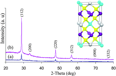
The powder X-ray diffraction of the as deposited films from experiments at 360 and 400 °C are shown in Fig. 1. The material can be identified as tetragonal Cu2ZnSnS4 (ICDD: 26–0575 or 002–0672) stannite or kesterite. The diffraction peaks can be indexed to (112), (200), (220), (312), (008) and (332) reflections of tetragonal Cu2ZnSnS4 with preferred orientation along the (112) plane. PXRD pattern also confirmed the absence of any binary sulfides such as CuS, Cu2S, SnS, or SnS2.
 | ||
| Fig. 1 PXRD pattern of CZTS thin films deposited at a) 360 °C and b) 400 °C. Inset conventional unit cell structure of CZTS. | ||
Cu2ZnSnS4 can crystallize in both the kesterite (Ī4) and stannite (Ī4 2m) structures. The computed total energy value by FPLAPW method22 for kesterite phase is only ∼1.3 meV/atom lower in energy than for the corresponding stannite structure.23 Since the lattice parameters and the structures of kesterite and stannite are very similar, both phases may exist in the same system and it is difficult to identify either of them separately by powder X-ray diffraction data alone.22
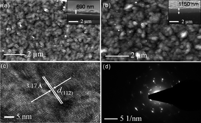
The SEM images of films deposited on glass substrate show closely packed granular crystallites with an average size of 150 nm at 360 °C and 200 nm at 400 °C (Fig. 2a, b). The cross-sectional SEM images show deposition of 690 nm thick films at 360 °C and 1150 nm at 400 °C (Fig. 2a,b, onset). The HRTEM image of sample obtained from the films deposited at 400 °C shows the lattice spacings of 3.17 Å corresponding to the (112) reflections of tetragonal kesterite Cu2ZnSnS4. The SAED pattern shows bright diffraction spots suggesting single crystalline nature of the films. Quantitative EDX measurements carried out with 20 KV energy source confirmed a 2![[thin space (1/6-em)]](https://www.rsc.org/images/entities/char_2009.gif) :
:![[thin space (1/6-em)]](https://www.rsc.org/images/entities/char_2009.gif) 1
1![[thin space (1/6-em)]](https://www.rsc.org/images/entities/char_2009.gif) :
:![[thin space (1/6-em)]](https://www.rsc.org/images/entities/char_2009.gif) 1.7
1.7![[thin space (1/6-em)]](https://www.rsc.org/images/entities/char_2009.gif) :
:![[thin space (1/6-em)]](https://www.rsc.org/images/entities/char_2009.gif) 4 stoichiometry for Cu2ZnSnS4 at 360 °C and 1.4
4 stoichiometry for Cu2ZnSnS4 at 360 °C and 1.4![[thin space (1/6-em)]](https://www.rsc.org/images/entities/char_2009.gif) :
:![[thin space (1/6-em)]](https://www.rsc.org/images/entities/char_2009.gif) 1.7
1.7![[thin space (1/6-em)]](https://www.rsc.org/images/entities/char_2009.gif) :
:![[thin space (1/6-em)]](https://www.rsc.org/images/entities/char_2009.gif) 1.2
1.2![[thin space (1/6-em)]](https://www.rsc.org/images/entities/char_2009.gif) :
:![[thin space (1/6-em)]](https://www.rsc.org/images/entities/char_2009.gif) 4 at 400 °C.
4 at 400 °C.
 | ||
| Fig. 2 SEM images of CZTS films deposited at a) 360 °C, b) 400 °C, c) HRTEM image, d) SAED pattern. Inset cross-sectional SEM images. | ||
The PXRD pattern of films deposited at 440 and 480 °C show the presence of small amounts of CuS which can be eliminated by reducing the concentration of copper precursor in the aerosol generator. The EDX showed the deposition of copper deficient and zinc rich films at higher temperatures (ESI†). Indeed, Cu-poor and Zn-rich conditions are sometimes used to improve solar cell efficiency.2,12,24
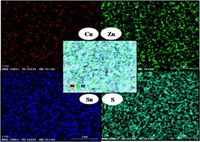
Elemental mapping by EDX (Fig. 3) shows that the Cu, Zn, Sn, and S are evenly distributed over the entire substrate. The absorption spectrum of the as-deposited CZTS thin films has been measured using UV-Vis absorbance spectroscopy (ESI†). The bandgap of the CZTS thin films is estimated to be 1.5 eV by extrapolating the linear region of a plot of the absorbance squared versus energy. This observed bandgap agrees well with those reported previously (1.3–1.51 eV).3,16 The variable temperature resistance measurement on the films deposited at 360 and 400 °C confirms the films are semiconducting with a resistance of 2 × 10⁶ Ω and 1.4 × 10⁶ Ω at room temperature (ESI†).
 | ||
| Fig. 3 EDX elemental mapping graph of films deposited at 360 °C. | ||
Good quality Cu2ZnSnS4 thin films have been deposited by AACVD for the first time using easily prepared diethyldithiocarbamato complexes of copper, zinc and tin. The deposited films were characterized by PXRD, SEM, TEM, SAED, EDX, UV-Vis spectroscopy and electrical resistivity measurements. Work on detailed cell performance with such films is being carried out and will be reported elsewhere.
Acknowledgements
KR is grateful to ORS and the University of Manchester for financial support. The authors also thank EPSRC, UK for grants to POB. We also thank Prof. Shozo Yanagida (Osaka) for suggesting POB take interest in this system.Notes and references
- H. Katagiri, Thin Solid Films, 2005, 515, 480; K. Jimbo, R. Kinura, T. Kamimura, S. Yamada, W. S. Maw, H. Araki, K. Oishi and H. Katagiri, Thin Solid Films, 2007, 5997 CrossRef CAS.
- A. Ennaoui, M. Lux-Steiner, A. Weber, D. Abou-Ras, I. Kotschau, H. W. Schock, R. Schurr, A. Holzing, A. Jost, R. Hock, T. Voß, J. Schulze and A. Kirbs, Thin Solid Films, 2009, 517, 2511 CrossRef CAS.
- K. Ito and T. Nakazawa, Jpn. J. Appl. Phys., 1988, 27, 2094 CrossRef CAS; H. Katagiri, K. Saitoh, T. Washio, H. Shinohara, T. Kurumadani and S. Miyajima, Sol. Energy Mater. Sol. Cells, 2001, 65, 141 CrossRef CAS; H. Matsushita, T. Maeda, A. Katsui and T. Takizawa, J. Cryst. Growth, 2000, 208, 416 CrossRef CAS.
- A. Weber, R. Mainz and H. W. Schock, J. Appl. Phys., 2010, 107, 013516 CrossRef.
- S. Chen, X. G. Gong, A. Walsh and S. H. Wei, Phys. Rev. B: Condens. Matter Mater. Phys., 2009, 79, 165211 CrossRef.
- T. K. Todorov, K. B. Reuter and D. B. Mitzi, Adv. Mater., 2010, 22, E156 CrossRef CAS.
- J. Seol, S. Lee, J. Lee, H. Nam and K. Kim, Sol. Energy Mater. Sol. Cells, 2003, 75, 155 CrossRef CAS.
- T. Tanaka, D. Kawasaki, M. Nishio, Q. Guo and H. Ogawa, Phys. Status Solidi C, 2006, 3, 2844 Search PubMed.
- T. Tanaka, T. Nagatomo, D. Kawasaki, M. Nishio, Q. Guo, A. Wakahara, A. Yoshida and H. Ogawa, J. Phys. Chem. Solids, 2005, 66, 1978 CrossRef CAS.
- M. Kurihara, D. Berg, J. Fisher, S. Siebetrit and P. J. Dale, Phys. Status Solidi C, 2009, 6, 1241 Search PubMed.
- K. Moriya, J. Watabe, K. Tanaka and H. Uchiki, Phys. Status Solidi C, 2006, 3, 2848 Search PubMed.
- K. Tanaka, M. Oonuki, N. Moritake and H. Uchiki, Sol. Energy Mater. Sol. Cells, 2009, 93, 583 CrossRef CAS.
- M. Y. Yeh, C. C. Lee and D. S. Wuu, J. Sol-Gel Sci. Technol., 2009, 52, 65 CrossRef CAS.
- K. Moriya, K. Tanaka and H. Uchiki, Jpn. J. Appl. Phys., 2007, 46, 5780 CrossRef CAS.
- N. Nakayama and K. Ito, Appl. Surf. Sci., 1996, 92, 171 CrossRef CAS; N. Kamoun, H. Bouzouita and B. Rezig, Thin Solid Films, 2007, 515, 5949 CrossRef CAS.
- Q. Guo, H. W. Willhouse and R. Agarwal, J. Am. Chem. Soc., 2009, 131, 11672 CrossRef CAS; S. C. Riha, B. A. Parkinson and A. L. Prieto, J. Am. Chem. Soc., 2009, 131, 12054 CrossRef CAS; C. Steinhagen, M. G. Panthani, V. Akhavan, B. Goodfellow, B. Koo and B. A. Korgel, J. Am. Chem. Soc., 2009, 131, 12554 CrossRef CAS.
- N. Nakayama and K. Ito, Appl. Surf. Sci., 1996, 92, 171 CrossRef CAS; H. Katagiri, N. Sasaguchi, S. Hando, S. Hoshino, J. Ohashi and T. Yokota, Sol. Energy Mater. Sol. Cells, 1997, 49, 407 CrossRef CAS; Y. B. K. Kumar, P. U. Bhaskar, G. S. Babu and V. S. Raja, Phys. Status Solidi A, 2010, 207, 149 CrossRef CAS; P. A. Fernandes, P. M. P. Salome and A. F. D. Cunha, Thin Solid Films, 2009, 517, 2519 CrossRef CAS; H. Yoo and J. H. Kim, Thin Solid Films, 2010, 518, 6567 CrossRef CAS.
- A. C. Jones, P. O'Brien, CVD of Compound Semiconductors:Precursor synthesis, Development and Applications, VCH, 1997, Weinheim, Cambridge, UK Search PubMed.
- R. E. Bailey and S. M. Nie, J. Am. Chem. Soc., 2003, 125, 7100 CrossRef CAS.
- A. C. Jones, T. J. Leedham, P. J. Wright, D. J. Williams, M. J. Crosbie, H. O. Davis, K. A. Fleeting and P. O'Brien, J. Eur. Ceram. Soc., 1999, 19, 1431 CrossRef CAS; K. A. Fleeting, P. O'Brien, D. J. Otway, A. J. P. White, D. J. Williams and A. C. Jones, Inorg. Chem., 1999, 38, 1432 CrossRef CAS; A. C. Jones, T. J. Leedham, H. O. Davies, K. A. Fleeting, P. O'Brien, M. J. Crosbie, P. J. Wright, D. J. William and P. A. Lane, Polyhedron, 2000, 19, 351 CrossRef CAS.
- J. McAleese, P. O'Brien and J. D. Otway, Chem. Vap. Deposition, 1998, 4, 94 CrossRef CAS; D. Fan, M. Afzaal, M. A. Malik, C. Q. Nguyen, P. O'Brien, P. J. Thomas, Coord.Chem. Rev, 2007, 251, p. 1878 Search PubMed.
- Full potential linearized augmented plane wave method.
- C. Persson, J. Appl. Phys., 2010, 107, 053710 CrossRef.
- H. Katagiri, K. Jimbo, W. S. Maw, K. Oishi, M. Yamazaki, H. Araki and A. Takeuchi, Thin Solid Films, 2009, 517, 2455 CrossRef CAS.
Footnote |
| † Electronic supplementary information (ESI) available: Experimental details, additional SEM images, PXRD pattern, EDX graph, variable temperature resistivity measurements. See DOI: 10.1039/c0sc00538j |
| This journal is © The Royal Society of Chemistry 2011 |
