
 Open Access Article
 This Open Access Article is licensed under a Creative Commons Attribution-Non Commercial 3.0 Unported Licence
Cu-modified electrolyte-gated transistors based on reduced graphene oxide†
Rafael Cintra
Hensel
 ad,
Nicola
Comisso
b,
Marco
Musiani
b,
Francesco
Sedona
a,
Mauro
Sambi
a,
Andrea
Cester
c,
Nicolò
Lago
c and
Stefano
Casalini
*a
ad,
Nicola
Comisso
b,
Marco
Musiani
b,
Francesco
Sedona
a,
Mauro
Sambi
a,
Andrea
Cester
c,
Nicolò
Lago
c and
Stefano
Casalini
*a
aDepartment of Chemical Sciences (DiSC), University of Padua, via Marzolo 1, 35131, Padua, Italy. E-mail: stefano.casalini@unipd.it
bInstitute of Condensed Matter Chemistry and Technologies for Energy (ICMATE), National Research Council (CNR), Corso Stati Uniti 4, 35127, Padua, Italy
cDepartment of Information Engineering (DEI), University of Padua, via Gradenigo 6/b, 35131, Padua, Italy
dSão Carlos Institute of Physics, University of São Paulo, Avenida Trabalhador São Carlense 400, 13566-590, São Carlos, Brazil
First published on 12th June 2023
Abstract
Electrolyte-gated transistors (EGTs) have attracted extensive attention due to their versatility and excellent performance in different fields of electronics. Here, we report on coplanar EGTs based on reduced graphene oxide (rGO), whose gates (flexible Au micro-electrodes) were modified by electrodeposition of either compact or porous Cu coatings (Cu-modified EGTs). The Cu coatings yielded a dramatic change in the minimum gate voltage spanning from −50 mV to −300 mV, which allowed extremely versatile tuning of the device signal. Furthermore, steady measurements led us to carry out prolonged measurements (>2 hours) under a constant bias in NaCl 0.1 M solution which was driven onto the EGTs by using homemade paper fluidics. Transient characterization studies pointed out a potentiometric sensitivity of around 1–3 mV with a signal-to-noise ratio (SNR) close to 5–10 for both electron and hole transport regimes. Since the response time of our Cu-modified EGTs was as low as 80 ms, we succeeded in monitoring emulated action potential (eAP) featuring a characteristic frequency equal to 0.1 Hz.
Introduction
Since the pioneering work of Wrighton et al.,1,2 electrolyte-gated transistors (EGTs) have attracted the attention of many scientists because these electronic devices possess interesting features such as low operational voltages, excellent compliance towards inorganic and organic semiconductors, versatile manufacturing capable of supporting sustainable electronics (viz. green and biocompatible electronics), etc.3–16In particular, EGTs consist of three terminals (i.e., source, drain and gate electrodes), with a semiconductor material that electrically bridges the drain and source terminals. According to the type of semiconductor, they can be identified as either electrolyte-gated field-effect transistors (EGFETs) or electrochemical transistors (ECTs).15 Although the boundary between these two classes of devices is rather elusive, the ion penetration into the semiconducting thin film plays a key role, either triggering faradaic reactions or simply establishing an electrical double-layer.
Several efforts have been made by the scientific community towards three macro-areas:13–15 (i) an ever-increasing exploration of natural and bio-inspired materials;4,5,7,17 (ii) the surface engineering of the electro-active interfaces (viz. semiconductor/electrolyte, gate/electrolyte etc.)10,13,14,17–21 and (iii) a stepwise sophistication of the device layout.22–29 For instance, an appealing combination of natural and biocompatible materials such as paper, starch, ethylcellulose and nanoparticle-based ink was demonstrated to fabricate all-printed EGTs that can be possibly transferred to any surface of interest.5,30–32 Regarding surface engineering, single-molecule detection has been demonstrated by functionalizing the gate terminal with specific antibodies able to detect antigens present in the serum.33 Another brilliant example is the use of the so-termed extended floating gate architecture introduced by Frisbie et al., who demonstrated the importance of controlling the area of the gate terminal coupled with an additional floating gate to endow EGTs with improved sensing capabilities towards ricin protein.22
Here, we focused our efforts on changing the physico-chemical properties of the Au gate surface via electrochemical deposition of either compact or compact/porous Cu layers. As a consequence, our method is placed at the border between two out of the three above-mentioned macro-areas, namely surface engineering and layout sophistication. Cu was selected for this study because, although less noble than Au, it is quite stable in aqueous media and reliable methods for the deposition of Cu layers with markedly different morphologies are available.34,35 We show that this approach dramatically changes the EGT performance because the deposition of Cu onto Au affects the work function of the gate terminal36 and the marked surface roughness factor of the porous Cu layer enhances the capacitance37 of the interface between an electrolyte and a gate. Compact Cu coatings, with a surface area comparable to that of the pristine Au gate, were obtained by the electrochemical reduction of Cu2+ ions from concentrated CuSO4/H2SO4 solutions at low current densities. Porous Cu coatings were deposited onto compact ones by hydrogen bubble templated cathodic electrodeposition38–47 of Cu, a method that allows increase the deposit surface area by at least 100 times.34,35 A concise description of the main features of hydrogen bubble templated cathodic electrodeposition is provided in the ESI.†
Furthermore, we exploited the features of the Nafion membrane, which is a cation-selective membrane often used in fuel cells.48–50 Nafion has already been used together with different types of (semi-)conducting materials51–53 (viz. graphene, GO and PEDOT:PSS) without affecting their electronic features, as it offers an additional shield against adventitious contaminants coming from the electrolyte or the outer environment. Since Cu is less noble than Au (i.e., pristine gate terminal), we decided to deposit Nafion also onto the gate terminal, beside the rGO thin film, in order to improve its corrosion resistance. By preventing the transport of aggressive anions towards the Cu surface, Nafion was expected to ensure long-lasting adhesion between Cu and the underlying polycrystalline Au and to improve the EGT stability.
By switching from pristine (i.e., polycrystalline Au gate) to Cu-modified EGTs, we observed a marked shift of the minimum gate voltage (i.e. −50 mV < ΔVG,min < −300 mV). Such a shift allowed for better tuning of both electron and hole transport with respect to the pristine device. This crucial aspect enables the versatile operation of these devices together with better potentiometric sensitivity. All these beneficial features led us to perform prolonged measurements (>2 hours of continuous recording) using homemade paper fluidics as well as the real-time monitoring of emulated action potentials (eAPs).
Experimental section
Electrodeposition of Cu coatings onto the gate electrode
We fabricated electrolyte-gated rGO thin film transistors on commercially available substrates consisting of Au micro-electrodes sputtered on polyethylene (PET), purchased from Metrohm-Dropsens.54 These devices comprise Au interdigitated electrodes (IDEs) with a gap of 30 μm, and a coplanar Au square 3 × 3 mm2 gate. A sketch of the system is shown in Fig. 1(a) and (b). | ||
| Fig. 1 (a) Vertical cross-section and (b) top view sketches of the EGT. (c) Sketch and photograph of the paper fluidic setup applied on the Cu-gated devices for long measurements by fluxing 0.1 M NaCl. | ||
The coplanar Au gate was modified by the electrodeposition of Cu with two distinct morphologies: compact (cCu) and porous (pCu). Electrolyses were performed by using the FET's gate as a cathode and a Pt wire as an anode, both immersed in the electrolytic solutions described below. The solutions, contained in an undivided glass cell, were vigorously stirred, in contact with the atmosphere and maintained at 25 °C using a thermostat.
A 0.88 M CuSO4 + 0.55 M H2SO4 solution was used to obtain compact Cu deposits. A constant 20 mA cm−2 cathodic current density was imposed. By transferring a charge of 10 C cm−2, layers with an estimated thickness of 3.7 μm were obtained.
Porous deposits were obtained, on top of the compact ones, using a 0.05 M CuSO4 + 0.30 M sodium citrate + 1.0 M (NH4)2SO4 solution, at a 1.0 A cm−2 cathodic current density. This mildly acid solution was preferred to the more often used CuSO4–H2SO4–CuCl2 solutions34 because, when exposed to the latter at an open circuit, the Au source and drain underwent a severe detachment from the plastic substrate. A 40 C cm−2 charge was transferred. Taking into account the low faradaic efficiency, caused by the concomitant hydrogen evolution, and the apparent density of the porous Cu,35 the layer thickness was estimated to be around 15–20 μm.
Deposition of the rGO-based thin-film
After the cCu- and pCu-based coatings, Au IDEs have been coated by the graphene oxide (GO) thin-film, as shown in Fig. 1(a) and (b). The GO suspension (4 mg mL−1, monolayer content >95%) was bought from Graphenea, and diluted in the proportion of 1![[thin space (1/6-em)]](https://www.rsc.org/images/entities/char_2009.gif) :10 v/v in bi-distilled water. For the GO deposition, we exploited the spontaneous adsorption of polyelectrolytes.55 To promote the adhesion of the polyelectrolytes on top of the device, we used a UV-ozone system for 15 minutes, which produced a negatively charged surface. Thus, as GO is negatively charged, we first immersed the substrate in a poly(diallylammonium chloride) solution (PDDA, Sigma Aldrich), 1% w/w, and 0.5 M NaCl, for 15 minutes. Then, after a careful rinse with bi-distilled water, we cast a GO droplet (5–10 μl) onto the IDEs for 3 h. Aiming at blocking the water evaporation, we placed this substrate in a plastic Petri dish containing a water reservoir and sealed it. Finally, we rinsed the samples in bi-distilled water and dried them using a nitrogen stream. For the electrochemical reduction of GO, a droplet of bi-distilled water was placed on top of the samples and grounded using an external Au electrode. The IDEs were short-circuited, and their potential was swept from 0 to −3 V, until achieving the expected grade of GO reduction. Moreover, two different droplets of Nafion 117 (∼5% in a mixture of lower aliphatic alcohols and water) were spin-coated at 2000 rpm for 1 minute onto the rGO and Cu-modified gate terminals, respectively.
:10 v/v in bi-distilled water. For the GO deposition, we exploited the spontaneous adsorption of polyelectrolytes.55 To promote the adhesion of the polyelectrolytes on top of the device, we used a UV-ozone system for 15 minutes, which produced a negatively charged surface. Thus, as GO is negatively charged, we first immersed the substrate in a poly(diallylammonium chloride) solution (PDDA, Sigma Aldrich), 1% w/w, and 0.5 M NaCl, for 15 minutes. Then, after a careful rinse with bi-distilled water, we cast a GO droplet (5–10 μl) onto the IDEs for 3 h. Aiming at blocking the water evaporation, we placed this substrate in a plastic Petri dish containing a water reservoir and sealed it. Finally, we rinsed the samples in bi-distilled water and dried them using a nitrogen stream. For the electrochemical reduction of GO, a droplet of bi-distilled water was placed on top of the samples and grounded using an external Au electrode. The IDEs were short-circuited, and their potential was swept from 0 to −3 V, until achieving the expected grade of GO reduction. Moreover, two different droplets of Nafion 117 (∼5% in a mixture of lower aliphatic alcohols and water) were spin-coated at 2000 rpm for 1 minute onto the rGO and Cu-modified gate terminals, respectively.
Electrical and electrochemical characterization
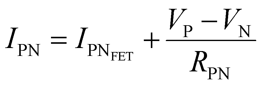
The devices were characterized in bi-distilled water and 0.1 M NaCl. All measurements were performed using a Faraday cage in the dark. An Agilent B1500 parameter analyzer equipped with two high-power and two high-resolution source measurement units (SMUs) was used for the transistor characterization. The I–V plots adopt the convention introduced by Lago et al.56,57 as it allows an unambiguous description of ambipolar EGTs. The positive (P) and negative (N) terminals act as holes–source/electrons–drain and electrons–source/holes–drain, respectively (i.e., VP ≥ 0 V, and VN < 0 V).58 Consequently, IP and IN are the currents measured through the P and N terminals, which allow us to record rigorously the overall functioning of our device (in our case, the P terminal is always grounded, namely VP = 0 V).The electrical characterization of the rGO-based EGTs has been carried out by the data fitting according to eqn (1).
 | (1) |
 , thus allowing us to compute the field effect current as
  . Then the p- and n-type threshold voltages (VTP and VTN), mobility enhancement factors (αP and αN), and field-effect mobilities (μFETP and μFETN) where extracted from
  in unipolar saturation regimes (p- and n-type, respectively) using the method reported in the literature56,57,59 with eqn (S1) (ESI†). This procedure is then iterated by changing the value of
  to minimize the least square error.
To determine the response time, we exploited high VGP pulses (i.e., VGP = VG − VP, ΔVGP > 100 mV), in such a way that the EGT was operated at potentials corresponding to the lowest and the highest transconductances  . To assess the potentiometric sensitivity, we took advantage of rather small VGP steps (i.e. ΔVGP < 20 mV) thereby aiming to define the smallest detectable potential change in the electrolyte.
To characterize the charge/discharge properties of the cCu-modified and pCu-modified EGTs, two kinds of tests were performed, using a Metrohm Autolab Potentiostat-Galvanostat PGSTAT302N. The source and drain electrodes were short-circuited, thereby acting as the counter electrode and the gate as the working electrode. The devices were submitted to standard cycles of charge/discharge by fixing Icharge = −Idischarge = 5 μA. Furthermore, we performed a stepwise protocol composed of the following steps: (i) charging process (Icharge = 5 μA), (ii) holding state (30 s at VGP = 300 mV), (iii) open circuit potential (60 s) and (iv) discharging process (Idischarge = −5 μA).
The eAP recording featured an amplitude of 115 mVpp and a frequency of 0.1 Hz using a waveform generator Rigol DG1022. In particular, we superimposed to the gate voltage an eAP based on the Hodkin–Huxley model.60
The prolonged electrical stress was investigated using a lab paper to drive the electrolyte, i.e., 0.1 M NaCl, onto our EGT (see the sketch in Fig. 1(c)). This setup mimics standard fluidics usually built exploiting polymers such as poly(dimethylsiloxane) – PDMS, which allowed us to perform electrical tests lasting some hours without any problems of solvent evaporation. Our characterization relied on recording the current of our EGT as a function of time by fixing VGP = −250 mV, VN = −300 mV and VP = 0 V.
The results shown in the next section were essentially reproduced with at least 5 independent devices.
Results and discussion
Preparation and characterization of EGTs with Cu-modified gates
Our EGT relies on the electronic features of rGO, and its manufacturing is completely described elsewhere.61,62 The main novelties described in this paper are the electrodeposition of Cu onto the planar gate and the use of an additional layer of Nafion cast on top of the rGO-based thin-film and the gate terminal (see Fig. 1(a) and (b)).The deposition of cCu onto Au gates, according to the procedure described in the experimental section, was straightforward. The optical and SEM images (Fig. S1 in the ESI†) show a continuous and rather smooth Cu deposit. The AFM images (Fig. S2 in the ESI†) show that cCu had an increased roughness with respect to the pristine Au gate, reaching a 208 nm root mean square roughness (σrms), about twice higher than Au. The cCu thickness determined by profilometry was 3.5 μm, a value coherent with that estimated from the electrolysis charge (3.7 μm).
We encountered severe difficulties (i.e. an extensive detachment of the Au deposit from the PET substrate) when we attempted the direct electrodeposition of pCu onto the Au gate because the required high current density induced delamination of the Au layers from the underlying PET substrate. However, we succeeded in depositing pCu on top of the compact layer, thus obtaining the pCu-modified gates described below. Details of the electrodeposition of pCu onto FET gates are described in the ESI.†
The SEM images of pCu deposits show a macroporous structure similar but not identical to those observed when electrodeposition was performed from CuSO4/H2SO4/CuCl2 solutions on bulky electrodes.35,47 The large pores are less deep and cover the electrode surface less homogeneously. However, the higher magnification images (Fig. S3(a)–(c), ESI†) prove that the Cu deposit obtained from the sulfate-citrate medium consists of an assembly of nanowires, ensuring porosity on the nanometric scale and a large surface roughness factor. To explain fine morphological differences, it is worth observing that the Cu deposition mechanism may not be identical in sulfate–citrate solution and sulfate–chloride solution, due to differences in their initial pH values (ca. 5 and below 1, respectively). In the former, under vigorous hydrogen evolution, the local pH increases and so, besides being directly reduced to Cu, Cu2+ may undergo hydrolysis to form CuO, eventually reduced to Cu. Probably, markedly different hydrodynamic conditions, which strongly influenced H2 bubble release, also contributed to determining morphological differences. The pCu deposit thickness assessed by profilometry was 20 μm. Its mean square roughness could not be determined, as it was well above the upper limit measurable by AFM.
The final step consisted of depositing the GO-based thin film onto the IDEs together with its electrochemical reduction to achieve the rGO.
I–V transfer characteristics
Electrical characterization has been performed by recording standard I–V transfer characteristics in both Milli-Q water (Fig. 2) and 0.1 M NaCl (Fig. S4 in the ESI†), because the former gives preliminary clues on the Cu-modified EGT performance, whereas the latter provides relevant information on their operation in more demanding environments, similar to real matrixes. Although the standard convention is well-established for both unipolar and ambipolar transistors, we adopted a specific convention recently proposed by N. Lago et al.56,57 in order to define unambiguously the injection/collection of electrons/holes in our ambipolar EGTs based on rGO. | ||
| Fig. 2 I–V transfer characteristics of the rGO device featuring the (a) pristine Au, (b) cCu-modified Au gate, (c) pCu-modified Au gate recorded in Milli-Q water. The red curve stands for the leakage current (IG) and the blue one stands for the current recorded at the P terminal (IP). VP = 0 V and VN = −300 mV. VGP and VGN = (VG − VN) ranges are presented as the bottom and top x-axis, respectively. | ||
Fig. 2(a)–(c) show the I–V transfer characteristics obtained in Milli-Q water for pristine, cCu-, and pCu-modified EGTs, in which VN = −300 mV and VP = 0 V (i.e., the common terminal for both gate and N terminals), and the gate potential VGP was swept from −300 mV to +300 mV. Albeit the ambipolar behaviour of graphene and its derivatives is known, the pristine Au gate transistor shows mainly hole conduction. This trend agrees with previous flexible EGTs featuring a coplanar liquid gate.62 cCu- and pCu-modified EGTs show the improved conduction of the electrons/holes. Both conduction branches (viz. p- and n-type regimes) are clearly defined due to the dramatic change of VG,min (i.e. −50 mV < ΔVG,min < −100 mV). This negative VG,min shift (i.e., negative doping) strengthens the electron conduction compared to the pristine EGT and may be ascribed to the change in the gate work function, as already observed by Kergoat et al.36 Further proof of the better performance of the Cu-modified EGTs than the reference one is the appropriate control of VG,min according to the VN variation (Fig. S5a–c in the ESI†).58 Coherently to these observations, the use of 0.1 M NaCl causes a relevant shift in the operational voltages of Cu-modified gate devices, whereas the pristine Au gate device is unaffected, as a result of its poor electronic modulation (see Fig. S4, ESI†). Comparing pristine EGTs with cCu/pCu-modified ones, ΔVG,min is also amplified with respect to bi-distilled water, spanning from −200 mV to −300 mV. Among the possible reasons for this change in performance between bi-distilled water and 0.1 M NaCl, one of the most relevant is the more efficient electrostatic screening of mobile or fixed charges around the conductive channel of the EGT, since electrostatic screening is strictly related to the Debye length (i.e. a shortening of the Debye length at a higher ionic strength).63 According to the I–V transfer characteristics, the mobility and threshold voltages of holes (μh, Vth,P) and electrons (μe, Vth,N) have been calculated by using eqn (S1) (ESI†) which describes ambipolar transistors, as reported elsewhere.56,57 Our data (Table S1, ESI†) provide an accurate characterization of these EGTs by changing systematically the electrolyte (bi-distilled water vs. 0.1 M NaCl) and the values of VN.
Investigation of transient phenomena
To achieve a more comprehensive view of the performance of Cu-modified EGTs, we performed a further investigation on transient phenomena such as the response time, potentiometric sensitivity, and capability to store/deliver charge. These technological issues are pivotal for the development of electronic devices operated like transducers capable of recording biological/bio-physical events (e.g., antibody–antigen pairing, neuronal spikes, heartbeats, and the release of drugs).64–69We determined the response time and potentiometric sensitivity of EGTs by recording IP as a function of time, in response to VGP pulses of variable magnitude, by using 0.1 M NaCl as the electrolyte. Fig. 3(a) and Fig. S6 in the ESI† (relevant to p- and n-type conduction, respectively) show that the experimental IP decay may be accurately fit by using eqn (2) which exploits the sum of two exponentials.
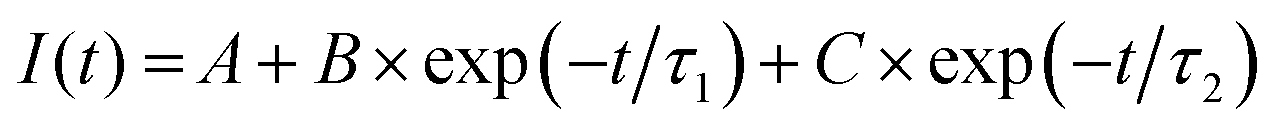 | (2) |
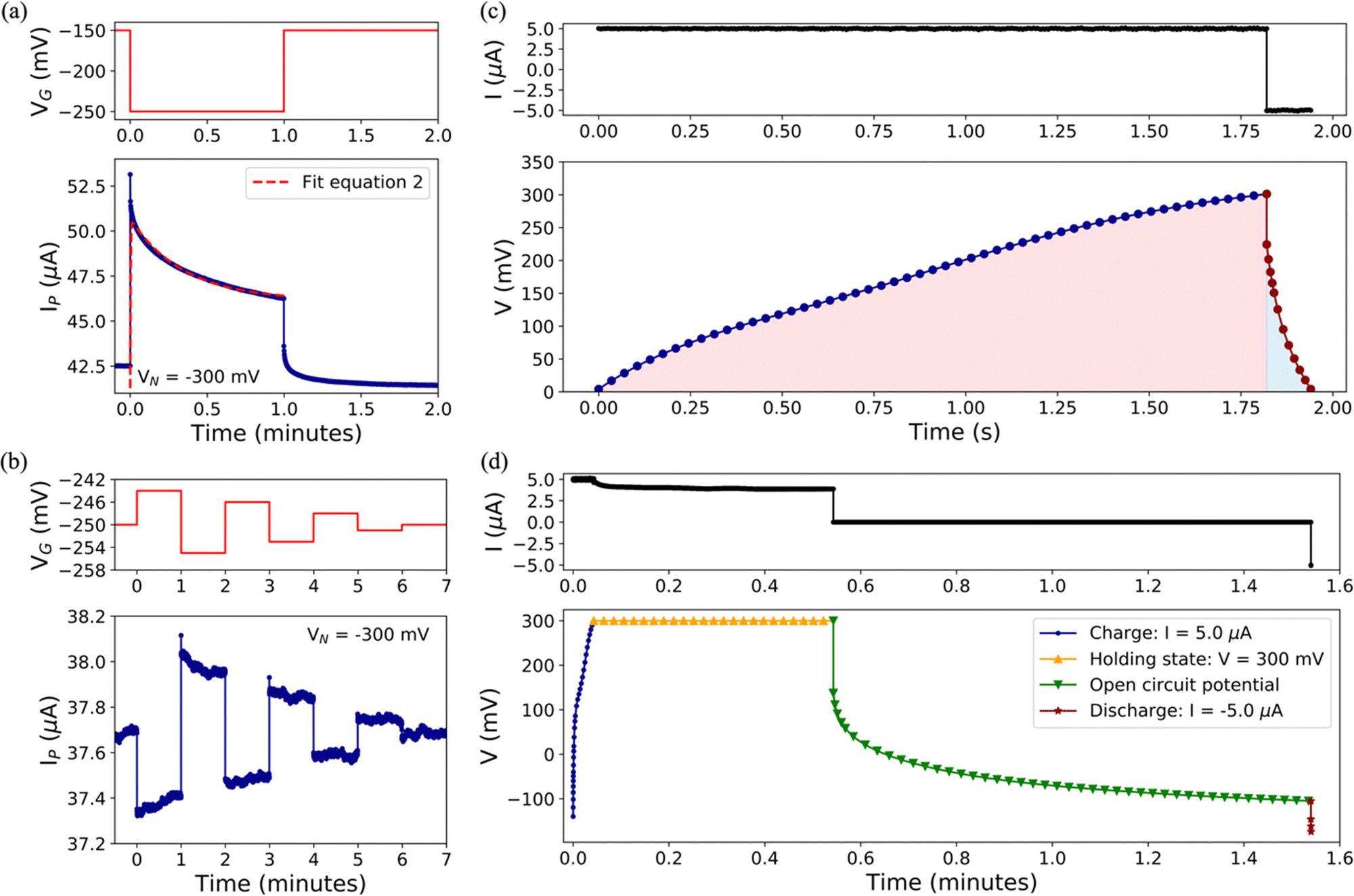 | ||
| Fig. 3 (a) Response time (the red dashed line is the fit), (b) potentiometric sensitivity and (c) and (d) galvanostatic charge/discharge of the pCu-gated EGT. All measurements are performed in NaCl 0.1 M. | ||
Regarding the potentiometric sensitivity, Fig. 3(b) and Fig. S7 (ESI†) show that pCu-modified EGTs are the most sensitive because they reach the highest signal-to-noise ratio (SNR), i.e., 5.8 and 12, for the p- and n-branches, respectively, and the lowest recordable VGP step, namely 1 mV and 3 mV for holes and electrons, respectively (see Table S2, ESI†). This can be ascribed to the increased roughness of the pCu coating with respect to both the pristine Au and cCu gate terminals. This leads to a more efficient electrical double layer at the gate interface, which enhances the amplification feature of the pCu-modified EGT.
Aiming at gaining more insights into the role played by Cu related to these performances, we performed standard cycles of charge/discharge with Icharge = −Idischarge = 5 μA, which is a standard value of the leakage current (viz. IG). The non-linear trend hints at pseudo-capacitor behaviour, instead of a simple capacitor, for both pCu- (Fig. 3(c)) and cCu-based (Fig. S8, ESI†) coatings.71 The coulombic efficiency (viz. Qdischarge/Qcharge) was higher for pCu (7.7%) than that for cCu (5.4%), due to its pronounced porosity and true surface area. Further tests have been carried out according to the protocol described in the Experimental section, which involved a holding step at a constant VGP = 300 mV and an open circuit step between the charging and discharging steps, allowing us to highlight the different efficiencies for cCu and pCu. The leakage current at a fixed VGP was more pronounced for cCu than pCu, decreasing from 5 μA to 2.9 μA and 3.9 μA, respectively. During the open circuit step, the decrease of the voltage was faster for cCu than pCu (further details in the ESI†). Moreover, the charge/discharge protocol allowed us to extract energy and power involved in the device's functioning (see Table S2, ESI†).
Recording of the emulated action potential and response to prolonged electrical stress
Aiming at more technologically relevant applications, we submitted our EGTs towards two tests: (i) recording of the emulated action potential (eAP) and (ii) prolonged electrical monitoring. Other types of (semi-)conducting materials,64,65,72,73 implemented in the EGT layout succeeded towards the real-time monitoring of biological signalling. According to the VGP set point (i.e., +250 mV and −250 mV) of the eAP, the user can select the n- or p-type conduction (see Fig. S9, ESI†). The former shows an increase in IP related to the eAP; in contrast, the latter shows an IP decrease (see Fig. 4). As a result, the pCu-modified EGT succeeded in recording the eAP for both types of conduction, whereas the cCu-modified one showed only a partial recording for p-type conduction (see Fig. S10, ESI†), which is coherent with the potentiometric sensitivity previously shown (see Fig. S7d, ESI†).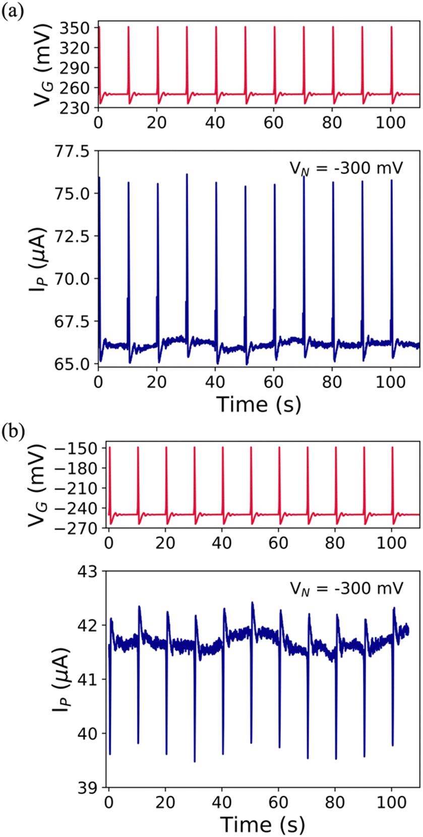 | ||
| Fig. 4 Emulated AP iterative series (red lines) and its recorded AP iterative series (blue lines) featuring (a) +250 mV set point potential and (b) −250 mV set point potential in NaCl 0.1 M. | ||
The prolonged electrical monitoring shows that IP decreases over time following two distinct processes: (i) one faster within 50 s, and (ii) another slower for the rest of the measurement, as depicted in Fig. 5, until IP stabilizes at ∼36.7 μA, after 2 hours. Such long-term measurement is an important issue to consider towards the real-time monitoring of a particular environment for biological and chemical purposes. A fingerprint for the stable functioning of the device even after prolonged tests (>2 hours) is the conservation of almost identical I–V transfer characteristics as shown in Fig. S11 (ESI†). We can safely rule out any faradaic reaction that might damage the device. Similar behaviour has been observed for the cCu-modified EGT operated under the same conditions (compare Fig. S12 in the ESI† with Fig. 5). In particular, these devices succeeded only by using VGP < 0 V (viz. hole conduction), because VGP > 0 V triggers the partial oxidation of the electrodeposited Cu, and its consequent electromigration onto the rGO thin film during prolonged measurements, thereby damaging the device.
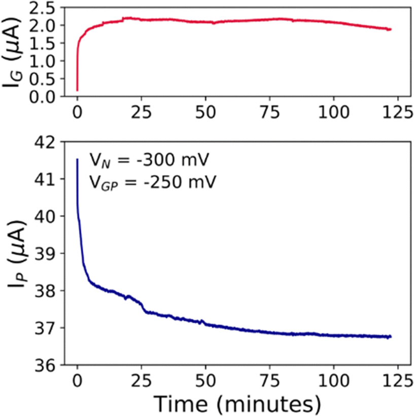 | ||
| Fig. 5 (a) IG and (b) IPvs. time plots for the prolonged electrical stress investigation, in which VN = −300 mV and VGP = −250 mV were fixed in 0.1 M NaCl. | ||
Conclusions
In this paper, we demonstrated how it is possible to couple the fabrication of an EGT based on the rGO thin film with the electrodeposition of Cu onto the ultrathin (viz. 20 nm thick) coplanar gate terminal. Two types of Cu coatings can be achieved: a compact (cCu) coating with a morphology resembling that of the underlying polycrystalline Au, and a porous (pCu) one, whose morphology shows a dual porosity. The Cu modification of the gate terminal shows the relevant n-doping of these EGTs, namely −50 mV < ΔVG,min < −300 mV according to different electrolytes and operational voltages. This allows extreme versatility in the Cu-modified EGT operation. As a result, we succeeded in operating the device in NaCl 0.1 M, which has an ionic strength comparable to real matrixes such as tap water, seawater and biological fluids. Moreover, the pCu-modified EGT showed a potentiometric sensitivity down to 1–3 mV for p- and n-type conduction, respectively, in a time scale of <1 s and a SNR of ≅6–10. For these reasons, it has been possible to track emulated action potentials (eAPs) with a characteristic frequency of 0.1 Hz. Prolonged tests (>2 hours) carried out using homemade paper fluidics showed satisfactory stability without any significant damage. These promising outcomes offer a new perspective in terms of the surface engineering and layout sophistication of such EGTs, paving the way towards novel sensors and/or transducers.Author contributions
Rafael Cintra Hensel: data curation, formal analysis, investigation, validation, software, visualization, writing – original draft, and writing – review and editing. Nicola Comisso: investigation and data curation. Marco Musiani: resources and writing – review and editing. Francesco Sedona: resources and writing – review and editing. Mauro Sambi: resources, writing – review and editing, and funding acquisition. Andrea Cester: resources and writing – review and editing. Nicolò Lago: investigation, formal analysis, and software. Stefano Casalini: conceptualization, funding acquisition, investigation, methodology, project administration, resources, supervision, validation, writing – original draft, and writing – review and editing.Conflicts of interest
There are no conflicts to declare.Acknowledgements
The authors acknowledge the financial support from the Italian Ministry of Education, Universities, and Research through the project “Nanochemistry for Energy and Health, NexuS” – the national funding network termed “Dipartimenti di Eccellenza” awarded to the Department of Chemical Sciences at the University of Padua and the project P-DiSC#11NexuS_BIRD2020-UNIPD (CARBON-FET) led by Prof. Stefano Casalini. RCH acknowledges the research grant no. 2020/15095-0 from São Paulo Research Foundation - FAPESP (Brazil).References
- H. S. White, G. P. Kittlesen and M. S. Wrighton, J. Am. Chem. Soc., 1984, 106, 5375–5377 CrossRef CAS.
- E. W. Paul, A. J. Ricco and M. S. Wrighton, J. Phys. Chem., 1985, 89, 1441–1447 CrossRef CAS.
- M. Irimia-Vladu, Chem. Soc. Rev., 2014, 43, 588–610 RSC.
- A. S. Sharova and M. Caironi, Adv. Mater., 2021, 33, 2103183 CrossRef CAS PubMed.
- G. E. Bonacchini, C. Bossio, F. Greco, V. Mattoli, Y.-H. Kim, G. Lanzani and M. Caironi, Adv. Mater., 2018, 30, 1706091 CrossRef PubMed.
- M. Irimia-Vladu, E. D. Głowacki, G. Voss, S. Bauer and N. S. Sariciftci, Mater. Today, 2012, 15, 340–346 CrossRef CAS.
- A. S. Sharova, F. Melloni, G. Lanzani, C. J. Bettinger and M. Caironi, Adv. Mater. Technol., 2021, 6, 2000757 CrossRef.
- M. Irimia-Vladu, P. A. Troshin, M. Reisinger, L. Shmygleva, Y. Kanbur, G. Schwabegger, M. Bodea, R. Schwödiauer, A. Mumyatov, J. W. Fergus, V. F. Razumov, H. Sitter, N. S. Sariciftci and S. Bauer, Adv. Funct. Mater., 2010, 20, 4069–4076 CrossRef CAS.
- C. Sun, X. Liu, Q. Jiang, X. Ye, X. Zhu and R.-W. Li, Sci. Technol. Adv. Mater., 2023, 24, 2162325 CrossRef PubMed.
- G. Y. Wang, K. Lian and T.-Y. Chu, IEEE J. Electron Devices Soc., 2021, 9, 939–950 CAS.
- B. Shkodra, M. Petrelli, M. A. Costa Angeli, D. Garoli, N. Nakatsuka, P. Lugli and L. Petti, Appl. Phys. Rev., 2021, 8, 041325 CAS.
- H. Ling, D. A. Koutsouras, S. Kazemzadeh, Y. van de Burgt, F. Yan and P. Gkoupidenis, Appl. Phys. Rev., 2020, 7, 011307 CAS.
- F. Torricelli, D. Z. Adrahtas, Z. Bao, M. Berggren, F. Biscarini, A. Bonfiglio, C. A. Bortolotti, C. D. Frisbie, E. Macchia, G. G. Malliaras, I. McCulloch, M. Moser, T.-Q. Nguyen, R. M. Owens, A. Salleo, A. Spanu and L. Torsi, Nat. Rev. Methods Primers, 2021, 1, 66 CrossRef CAS PubMed.
- W. Huang, J. Chen, G. Wang, Y. Yao, X. Zhuang, R. M. Pankow, Y. Cheng, T. J. Marks and A. Facchetti, J. Mater. Chem. C, 2021, 9, 9348–9376 RSC.
- S. H. Kim, K. Hong, W. Xie, K. H. Lee, S. Zhang, T. P. Lodge and C. D. Frisbie, Adv. Mater., 2013, 25, 1822–1846 CrossRef CAS PubMed.
- S. Nandy, S. Goswami, A. Marques, D. Gaspar, P. Grey, I. Cunha, D. Nunes, A. Pimentel, R. Igreja, P. Barquinha, L. Pereira, E. Fortunato and R. Martins, Adv. Mater. Technol., 2021, 6, 2000994 CrossRef CAS.
- I. Cunha, R. Barras, P. Grey, D. Gaspar, E. Fortunato, R. Martins and L. Pereira, Adv. Funct. Mater., 2017, 27, 1606755 CrossRef.
- M. Berto, C. Diacci, R. D’Agata, M. Pinti, E. Bianchini, M. Di Lauro, S. Casalini, A. Cossarizza, M. Berggren, D. Simon, G. Spoto, F. Biscarini and C. A. Bortolotti, Adv. Biosyst., 2018, 2, 1700072 CrossRef.
- S. Casalini, F. Leonardi, T. Cramer and F. Biscarini, Org. Electron., 2013, 14, 156–163 CrossRef CAS.
- M. S. Thomas, S. P. White, K. D. Dorfman and C. D. Frisbie, J. Phys. Chem. Lett., 2018, 9, 1335–1339 CrossRef CAS PubMed.
- Y. S. Rim, H. Chen, B. Zhu, S.-H. Bae, S. Zhu, P. J. Li, I. C. Wang and Y. Yang, Adv. Mater. Interfaces, 2017, 4, 1700020 CrossRef.
- S. P. White, S. Sreevatsan, C. D. Frisbie and K. D. Dorfman, ACS Sens., 2016, 1, 1213–1216 CrossRef CAS.
- S. P. White, K. D. Dorfman and C. D. Frisbie, Anal. Chem., 2015, 87, 1861–1866 CrossRef CAS PubMed.
- S. P. White, K. D. Dorfman and C. D. Frisbie, J. Phys. Chem. C, 2016, 120, 108–117 CrossRef CAS.
- K. Fukuda, T. Minamiki, T. Minami, M. Watanabe, T. Fukuda, D. Kumaki and S. Tokito, Adv. Electron. Mater., 2015, 1, 1400052 CrossRef.
- M. S. Ozório, D. H. Vieira, G. L. Nogueira, C. S. Martin, N. Alves and C. J. L. Constantino, Mater. Sci. Semicond. Process., 2022, 151, 107045 CrossRef.
- M. Nikolka, D. Simatos, A. Foudeh, R. Pfattner, I. McCulloch and Z. Bao, ACS Appl. Mater. Interfaces, 2020, 12, 40581–40589 CrossRef CAS PubMed.
- D. Gaspar, J. Martins, P. Bahubalindruni, L. Pereira, E. Fortunato and R. Martins, Adv. Electron. Mater., 2018, 4, 1800423 CrossRef.
- R. Morais, D. H. Vieira, M. dos, S. Klem, C. Gaspar, L. Pereira, R. Martins and N. Alves, Semicond. Sci. Technol., 2022, 37, 035007 CrossRef.
- L. Santos, D. Nunes, T. Calmeiro, R. Branquinho, D. Salgueiro, P. Barquinha, L. Pereira, R. Martins and E. Fortunato, ACS Appl. Mater. Interfaces, 2015, 7, 638–646 CrossRef CAS PubMed.
- J. T. Carvalho, V. Dubceac, P. Grey, I. Cunha, E. Fortunato, R. Martins, A. Clausner, E. Zschech and L. Pereira, Nanomaterials, 2019, 9(2), 169 CrossRef CAS PubMed.
- P. I. C. Claro, I. Cunha, R. T. Paschoalin, D. Gaspar, K. Miranda, O. N. Oliveira Jr., R. Martins, L. Pereira, J. M. Marconcini, E. Fortunato and L. H. C. Mattoso, ACS Appl. Mater. Interfaces, 2021, 13, 26237–26246 CrossRef CAS PubMed.
- E. Macchia, K. Manoli, B. Holzer, C. Di Franco, M. Ghittorelli, F. Torricelli, D. Alberga, G. F. Mangiatordi, G. Palazzo, G. Scamarcio and L. Torsi, Nat. Commun., 2018, 9, 3223 CrossRef PubMed.
- N. Comisso, S. Cattarin, P. Guerriero, L. Mattarozzi, M. Musiani, L. Vázquez-Gómez and E. Verlato, J. Solid State Electrochem., 2016, 20, 1139–1148 CrossRef CAS.
- L. Mattarozzi, S. Cattarin, N. Comisso, A. Gambirasi, P. Guerriero, M. Musiani, L. Vazquez Gomez and E. Verlato, Electrochim. Acta, 2014, 140, 337–344 CrossRef CAS.
- L. Kergoat, L. Herlogsson, B. Piro, M. C. Pham, G. Horowitz, X. Crispin and M. Berggren, Proc. Natl. Acad. Sci. U. S. A., 2012, 109, 8394–8399 CrossRef CAS PubMed.
- M. Singh, K. Manoli, A. Tiwari, T. Ligonzo, C. Di Franco, N. Cioffi, G. Palazzo, G. Scamarcio and L. Torsi, J. Mater. Chem. C, 2017, 5, 3509–3518 RSC.
- H.-C. Shin, J. Dong and M. Liu, Adv. Mater., 2003, 15, 1610–1614 CrossRef CAS.
- H.-C. Shin and M. Liu, Chem. Mater., 2004, 16, 5460–5464 CrossRef CAS.
- N. D. Nikolić and K. I. Popov, in Electrodeposition: Theory and Practice, ed. S. S. Djokic, Springer, New York, NY, 2010, pp. 1–70 Search PubMed.
- Y. Li, W.-Z. Jia, Y.-Y. Song and X.-H. Xia, Chem. Mater., 2007, 19, 5758–5764 CrossRef CAS.
- D. Nam, R. Kim, D. Han, J. Kim and H. Kwon, Electrochim. Acta, 2011, 56, 9397–9405 CrossRef CAS.
- S. Cherevko, X. Xing and C.-H. Chung, Electrochem. Commun., 2010, 12, 467–470 CrossRef CAS.
- S. Cherevko and C.-H. Chung, Electrochim. Acta, 2010, 55, 6383–6390 CrossRef CAS.
- S. Cherevko and C.-H. Chung, Electrochem. Commun., 2011, 13, 16–19 CrossRef CAS.
- S. Cherevko, X. Xing and C.-H. Chung, Appl. Surf. Sci., 2011, 257, 8054–8061 CrossRef CAS.
- L. Mattarozzi, S. Cattarin, N. Comisso, P. Guerriero, M. Musiani and E. Verlato, Electrochim. Acta, 2016, 198, 296–303 CrossRef CAS.
- M. B. Karimi, F. Mohammadi and K. Hooshyari, Int. J. Hydrogen Energy, 2019, 44, 28919–28938 CrossRef CAS.
- X. Shi, Y. Ma, X. Huo, O. C. Esan and L. An, Int. J. Green Energy, 2021, 1–7 Search PubMed.
- F. A. Zakil, S. K. Kamarudin and S. Basri, Renewable Sustainable Energy Rev., 2016, 65, 841–852 CrossRef CAS.
- Z. Wang, Z. Hao, X. Wang, C. Huang, Q. Lin, X. Zhao and Y. Pan, Adv. Funct. Mater., 2021, 31, 2005958 CrossRef CAS.
- S. J. Lue, Y.-L. Pai, C.-M. Shih, M.-C. Wu and S.-M. Lai, J. Membr. Sci., 2015, 493, 212–223 CrossRef CAS.
- P.-P. Lu, D.-S. Shang, C.-S. Yang and Y. Sun, J. Phys. D: Appl. Phys., 2020, 53, 485102 CrossRef CAS.
- Flexible Gold Field-Effect Transistors with coplanar gate, https://www.dropsens.com/en/pdfs_productos/new_brochures/aufet30.pdf, (accessed 9 February 2023).
- G. Decher, Science, 1979, 1997(277), 1232–1237 Search PubMed.
- N. Lago, M. Buonomo, R. C. Hensel, F. Sedona, M. Sambi, S. Casalini and A. Cester, IEEE Trans. Electron Devices, 2022, 69, 3192–3198 CAS.
- N. Lago, M. Buonomo, R. C. Hensel, F. Sedona, M. Sambi, S. Casalini and A. Cester, IEEE Trans. Electron Devices, 2022, 69, 6492 Search PubMed.
- S. Lee, A. Nathan, J. Alexander-Webber, P. Braeuninger-Weimer, A. A. Sagade, H. Lu, D. Hasko, J. Robertson and S. Hofmann, ACS Appl. Mater. Interfaces, 2018, 10, 10618–10621 CrossRef CAS PubMed.
- P. Servati, D. Striakhilev and A. Nathan, IEEE Trans. Electron Devices, 2003, 50, 2227–2235 CrossRef CAS.
- A. L. Hodgkin and A. F. Huxley, J. Physiol., 1952, 117, 500–544 CrossRef CAS PubMed.
- R. Furlan de Oliveira, V. Montes-García, P. A. Livio, M. B. González-García, P. Fanjul-Bolado, S. Casalini and P. Samorì, Small, 2022, 18, 2201861 CrossRef CAS PubMed.
- R. Furlan de Oliveira, P. A. Livio, V. Montes-García, S. Ippolito, M. Eredia, P. Fanjul-Bolado, M. B. González García, S. Casalini and P. Samorì, Adv. Funct. Mater., 2019, 29(46), 1905375 CrossRef CAS.
- T. Xiao and X. Song, J. Chem. Phys., 2011, 135, 104104 CrossRef PubMed.
- A. Campana, T. Cramer, D. T. Simon, M. Berggren and F. Biscarini, Adv. Mater., 2014, 26, 3874–3878 CrossRef CAS PubMed.
- T. Cramer, B. Chelli, M. Murgia, M. Barbalinardo, E. Bystrenova, D. M. de Leeuw and F. Biscarini, Phys. Chem. Chem. Phys., 2013, 15, 3897–3905 RSC.
- S. Casalini, A. C. Dumitru, F. Leonardi, C. A. Bortolotti, E. T. Herruzo, A. Campana, R. F. de Oliveira, T. Cramer, R. Garcia and F. Biscarini, ACS Nano, 2015, 9, 5051–5062 CrossRef CAS PubMed.
- R. A. Picca, K. Manoli, E. Macchia, L. Sarcina, C. Di Franco, N. Cioffi, D. Blasi, R. Österbacka, F. Torricelli, G. Scamarcio and L. Torsi, Adv. Funct. Mater., 2020, 30, 1904513 CrossRef CAS.
- E. Macchia, R. A. Picca, K. Manoli, C. Di Franco, D. Blasi, L. Sarcina, N. Ditaranto, N. Cioffi, R. Österbacka, G. Scamarcio, F. Torricelli and L. Torsi, Mater. Horiz., 2020, 7, 999–1013 RSC.
- G. Foschi, F. Leonardi, A. Scala, F. Biscarini, A. Kovtun, A. Liscio, A. Mazzaglia and S. Casalini, Nanoscale, 2015, 7, 20025–20032 RSC.
- G. C. Faria, D. T. Duong and A. Salleo, Org. Electron., 2017, 45, 215–221 CrossRef CAS.
- T. S. Mathis, N. Kurra, X. Wang, D. Pinto, P. Simon and Y. Gogotsi, Adv. Energy Mater., 2019, 9, 1902007 CrossRef CAS.
- L. H. Hess, M. Jansen, V. Maybeck, M. V. Hauf, M. Seifert, M. Stutzmann, I. D. Sharp, A. Offenhäusser and J. A. Garrido, Adv. Mater., 2011, 23, 5045–5049 CrossRef CAS PubMed.
- A. Kyndiah, F. Leonardi, C. Tarantino, T. Cramer, R. Millan-Solsona, E. Garreta, N. Montserrat, M. Mas-Torrent and G. Gomila, Biosens. Bioelectron., 2020, 150, 111844 CrossRef CAS PubMed.
Footnote |
| † Electronic supplementary information (ESI) available. See DOI: https://doi.org/10.1039/d3tc00596h |
| This journal is © The Royal Society of Chemistry 2023 |