
High broadband photoconductivity of few-layered MoS2 field-effect transistors measured using multi-terminal methods: effects of contact resistance†
 c
Qilin
Dai,
a
Paresh C.
Ray,
a
Bhausaheb
Tawade,
e
Alamgir
Karim
f
and
Nihar R.
Pradhan
*ad
c
Qilin
Dai,
a
Paresh C.
Ray,
a
Bhausaheb
Tawade,
e
Alamgir
Karim
f
and
Nihar R.
Pradhan
*ad
Abstract
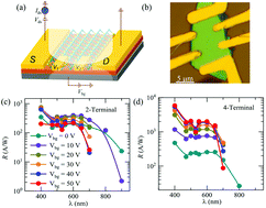
Among the layered two dimensional semiconductors, molybdenum disulfide (MoS2) is considered to be an excellent candidate for applications in optoelectronics and integrated circuits due to its layer-dependent tunable bandgap in the visible region, high ON/OFF current ratio in field-effect transistors (FET) and strong light–matter interaction properties. In this study, using multi-terminal measurements, we report high broadband photocurrent response (R) and external quantum efficiency (EQE) of few-atomic layered MoS2 phototransistors fabricated on a SiO2 dielectric substrate and encapsulated with a thin transparent polymer film of Cytop. The photocurrent response was measured using a white light source as well as a monochromatic light of wavelength λ = 400 nm–900 nm. We measured responsivity using a 2-terminal configuration as high as R = 1 × 10³ A W−1 under white light illumination with an optical power Popt = 0.02 nW. The R value increased to 3.5 × 10³ A W−1 when measured using a 4-terminal configuration. Using monochromatic light on the same device, the measured values of R were 103 and 6 × 10³ A W−1 under illumination of λ = 400 nm when measured using 2- and 4-terminal methods, respectively. The highest EQE values obtained using λ = 400 nm were 105% and 106% measured using 2- and 4-terminal configurations, respectively. The wavelength dependent responsivity decreased from 400 nm to the near-IR region at 900 nm. The observed photoresponse, photocurrent–dark current ratio (PDCR), detectivity as a function of applied gate voltage, optical power, contact resistances and wavelength were measured and are discussed in detail. The observed responsivity is also thoroughly studied as a function of contact resistance of the device.
- This article is part of the themed collection: 2020 Nanoscale HOT Article Collection
 Please wait while we load your content...

