
Art etching of graphene
Gayathri Devi
N
 a,
The-Hung
Mai
a,
Ram K.
Gupta
b and
Phuong V.
Pham
*a
a,
The-Hung
Mai
a,
Ram K.
Gupta
b and
Phuong V.
Pham
*a
aDepartment of Physics, National Sun Yat-sen University, Kaohsiung 80424, Taiwan. E-mail: phuongpham@mail.nsysu.edu.tw
bDepartment of Chemistry, Kansas Polymer Research Center, Pittsburg State University, Pittsburg, KS-66762, USA
First published on 3rd July 2024
Abstract
The growth of graphene on a metal substrate using chemical vapor deposition (CVD), assisted by hydrocarbons such as CH4, C3H8, C2H6, etc. leads to the formation of carbon clusters, amorphous carbon, or any other structure. These carbon species are considered as unwanted impurities; thus a conventional etching step is used simultaneously with CVD graphene growth to remove them using an etching agent. Meanwhile, art etching is a specific method of producing controlled non-Euclidean and Euclidean geometries by employing intricate and precise etching parameters or integrated growth/etching modes. Agents such as H2, O2, CH4, Ar, and others are applied as art etching agents to support the art etching technology. This technique can generate nanopores and customize the properties of graphene, facilitating specific applications such as nanodevices, nanosensors, nanofilters, etc. This comprehensive review investigates how precursor gases concurrently induce graphene growth and art etching during a chemical vapor deposition process, resulting in beautifully etched patterns. Furthermore, it discusses the techniques leading to the creation of these patterns. Finally, the challenges, uses, and perspectives of these non-Euclidean and Euclidean-shaped art etched graphene geometries are discussed.
 Gayathri Devi N. | Gayathri Devi N. is an intern under the supervision of Prof. Phuong V. Pham in the Material Physics and Electronic Surface Group, Department of Physics, National Sun Yat-Sen University, Taiwan. Her research interests focus on thin films and 2D materials for electronics. |
 The-Hung Mai | The-Hung Mai is an integrated MS/PhD candidate in Prof. Phuong V. Pham's Group at Department of Physics, National Sun Yat-sen University (NSYSU), Taiwan. He received his BS degree as Magna Cum Laude (2nd rank) in engineering physics, University of Engineering and Technology (UET), Vietnam National University (VNU), Hanoi (2021). His research interests include single crystalline growth, thin films, low-dimensional material synthesis, and thinning technology for electronics, optoelectronics, and green energy. |
 Ram K. Gupta | Ram K. Gupta is a Professor at Pittsburg State University (2013-present). Before joining Pittsburg State University, he worked as an Assistant Research Professor at Missouri State University, Springfield, MO, and then as a Senior Research Scientist at North Carolina A&T State University, Greensboro, NC. Dr Gupta is serving as an Associate Editor and reviewer for several leading science journals. His research focus is on green energy production and storage using nanomaterials, optoelectronic and photovoltaic devices, organic–inorganic hetero-junctions for sensors, nanomagnetism, conducting polymers and composites as well as bio-based polymers, bio-compatible nanofibers for tissue regeneration, scaffold and antibacterial applications and bio-degradable metallic implants. Dr Gupta has received a number of research grants (over one million dollars) from federal and state agencies such as National Science Foundation (NSF), NSF-Experimental Program to Stimulate Competitive Research (EPSCoR), Department of Energy (DoE), Kansas IDeA Network of Biomedical Research Excellence (K-INBRE), State of Kansas Polymer Chemistry Initiative, etc. |
 Phuong V. Pham | Phuong V. Pham is a Professor at the Department of Physics, National Sun Yat-sen University (NSYSU), Taiwan. He is leading the Materials Physics and Electronic Surfaces Group. He has joined the industrial projects with SAMSUNG, POSCO, the Korea Government, the Ministry of Education and Ministry of Science and Technology of China, and NSTC Grant (Taiwan). He has been a former Distinguished Research Fellow at the Hangzhou Global Scientific and Technological Innovation Center, Zhejiang University, China. He earned a PhD degree from SKKU Advanced Institute of Nanotechnology (SAINT), Sungkyunkwan University (SKKU), South Korea. Then, he spent a few years as a Postdoctoral Researcher and Research Fellow at the School of Advanced Materials Science and Engineering, SKKU, and at the Centre for Multidimensional Carbon Material (Director: Prof. Rodney Ruoff), Institute for Basic Science, South Korea, respectively. He is a recipient of the NSF Career Award, National Postdoctoral Award for Outstanding Yong Scientists, China (2019), and the NSTC Grant Award in Taiwan (2023). He has published over 70 peer-reviewed papers, books, and book chapters. His research interest focuses on nanotechnology, materials physics, chemical engineering, surface physics, atomic film syntheses, 2D heterostructures, donors/acceptors, nanocomposites, and plasma engineering for electronics/optoelectronics. |
1. Introduction
Graphene – a single hexagon layer of carbon atoms – was successfully isolated by A. Geim and K. Novoselov in 2004.1 Its notable features include high mobility,2,3 high mechanical strength,4,5 high flexibility,4,6,7 long wavelength, and high thermal conductivity.1,8 To utilize these remarkable properties in industrial applications, researchers face challenges in producing high-quality, uniform, and clean9,10 graphene integrated with these features at a commercial price for application in electronics,11–13 optoelectronics,12,14 photonics,12,15 and other domains.16 Unlike graphene, transition metal dichalcogenides (TMDs) exhibit semiconducting properties, especially good electrical conductivity. However, their synthesis can be more intricate, making graphene a potentially preferable option. Thus, graphene may perform well compared with TMDs.17–20 To create high-quality, homogenous graphene,6,21 one must comprehend the growth and kinetics of graphene.22–24 Numerous strategies have been employed e.g., chemical vapor deposition (CVD),25–28 liquid-phase exfoliation,29–32 plasma-enhanced CVD,33–36 and epitaxial growth of graphene.37 Among these techniques,38 CVD is one of the most frequently utilized processes to create consistent and superior-grade graphene nanofilms.Traditional art etching utilizes a similar CVD technique to produce complex and eye-catching designs on a clean surface. The art etching technique is inspired by the principles of the conventional etching technique used in a CVD process. From the beginning of 2010, the rate of usage of conventional graphene etching increased steadily until 2019 (Fig. 1). Several other techniques are used for conventional etching including ion beam etching (IBE),39 atomic layer etching (ALE),40 plasma etching,34,41,42 reactive ion etching (RIE)43,44 and laser-induced etching.45,46 However, these techniques are not commonly applied for integrated graphene growth/etching. Indeed, the CVD approach differs from these techniques, as it enables the concurrent growth and etching of graphene during the CVD process. A carbon source is utilized to grow such etched graphene on a metal substrate and various gases are used as art etching agents to etch graphene to produce art geometries (Fig. 2).47 In order to replicate the intricate and accurate etching modes seen in nature,47 contemporary technology is employed to imitate art geometries.47 Other than art etching, a few alternative methods are used, such as lithographic patterning,48,49 which can be employed in addition for patterned etching to create particular graphene configurations. Large-area five-lobed,50 alphabet letters48 and zigzag48 and triangular50 graphene grains were also found in previous investigation on textured liquid Cu substrates. However, this type of manufacturing requires a high concentration of H2, which might be hazardous and could lead to energy loss.
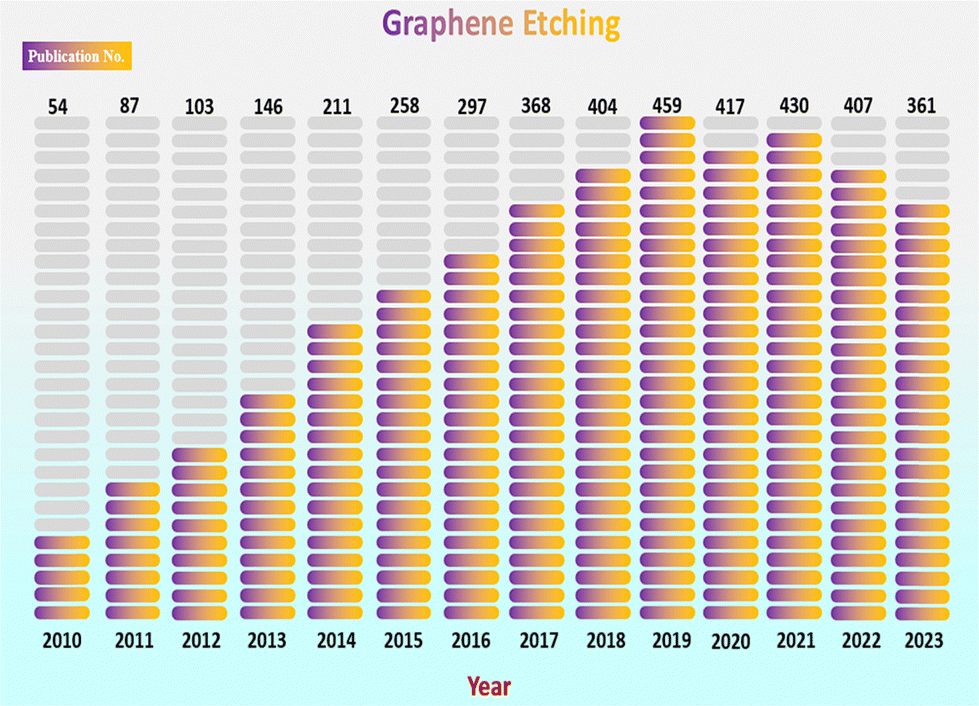 | ||
| Fig. 1 The textual analysis through annual publications of “Graphene Etching”. Source: Web of Science. | ||
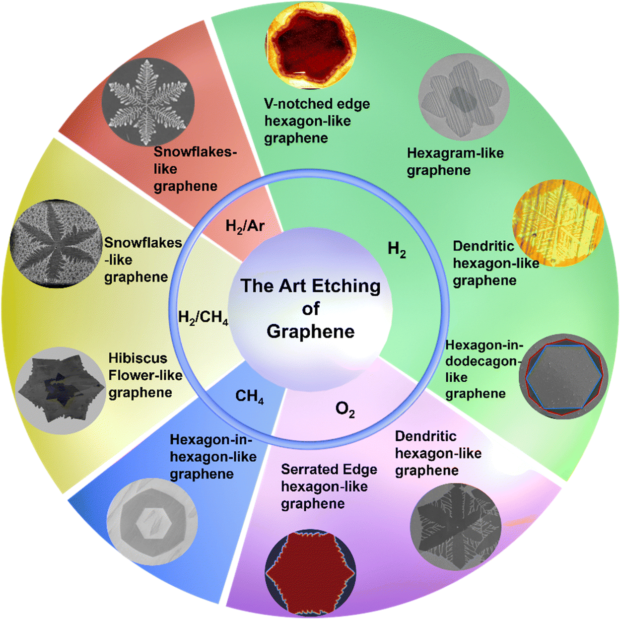 | ||
| Fig. 2 Structure shows different kinds of Euclidean and non-Euclidean geometries obtained during CVD graphene etching using various gases. (a) V-Notched edge hexagon-like graphene. Reproduced from ref. 47 with permission from American Chemical Society, copyright 2018. (b) Hexagram-like graphene. Reproduced from ref. 24 with permission from American Chemical Society, copyright 2011. (c) Dendritic hexagon-like graphene. Reproduced with permission from ref. 51 Royal Society of Chemistry, copyright 2018. (d) Hexagon-in-dodecagon-like Graphene. Reproduced from ref. 52 Copyright 2017 American Chemical Society, (e) dendritic hexagon-like graphene. Reproduced with permission from ref. 53 with permission from Elsevier, copyright 2013. (f) Serrated edge hexagon-like graphene. Reproduced from ref. 48 with permission from American Association for the Advancement of Science, copyright 2013. (g) Hexagon-in-hexagon-like graphene. Reproduced from ref. 54 with permission from National Academy of Sciences, copyright 2013. (h) Hibiscus flower-like graphene. Reproduced with permission from ref. 55 American Chemical Society, copyright 2017. (i) Snowflake-like graphene. Reproduced from ref. 56 with permission from American Chemical Society, copyright 2018. (j) Snowflake-like graphene. Reproduced from ref. 49 with permission from American Chemical Society, copyright 2013. | ||
This review addresses how different gases influence the development of distinct geometric structures of graphene, as well as the integrated growth and art etching of graphene during the CVD process. In this context, CH4 contributes to the formation of graphene, while H2,26,57 O2,58 and Ar59 are critical gases used as art etching agents. In addition to its various applications in electronics, optoelectronics, and spintronics, art-etched graphene can also form in-plane heterostructures with other 2D and 3D materials. Moreover, art etching aids in the development of graphene nanopores for nanofilters. However, the mechanism underlying these types of art etching remains unclear due to the different growth rates and shapes of graphene between different labs, even under similar growth conditions. To overcome this mystery, researchers employ a variety of systematic analyses, including density functional theory (DFT), and methods implemented using the Vienna ab initio simulation package (VASP),53,55 kinetic Monte Carlo simulations,51,52 kinetic Wulff construction theory,53 and phase-field model simulations,60 used for initial prediction of desirable graphene geometries. Finally, this comprehensive review also explores the potential mechanisms underlying the non-Euclidean and Euclidean graphene geometries.
2. Art etching strategies through the development to date
Material etching involves the spontaneous removal of components from a material matrix through a physical or chemical means and can often be seen as the reverse of the growth process at a microscopic level.54 Understanding this etching process is crucial for designing materials and achieving their desired functionalities. Both material growth and etching require a high-energy-barrier nucleation step followed by an easier pathway for expanding the formed nuclei. Generally, controlling the process parameters can lead to the spontaneous formation of thermodynamically stable ordered structures and various kinetically controlled metastable structures with high-energy crystalline facets or edges. This control has been demonstrated in many material growth systems across nanometer to macroscopic scales.56,61 Snowflakes are a fascinating example, with rich patterns formed via a nonlinear natural process.47 Conversely, it is widely accepted that perfectly crystalline materials are etched following a simple anisotropic rule, resulting in simple thermodynamically stable etched patterns with Euclidean geometries. This is due to different etching rates along different crystallographic surfaces or directions, which are associated with different free energies.2.1. V-notched edge hexagon-like graphene by H2-induced art etching
The formation of a V-notched hexagon-like Cu pattern (Fig. 3a–d) at a high H2 (100 sccm) concentration and a specific temperature (1090 °C) for 30 minutes is the result of integrated graphene growth and art etching on a liquid Cu/W substrate using a low-pressure chemical vapor deposition (LPCVD) process, as described by Pham et al.57 To induce the formation of graphene, the authors used CH4 as a precursor gas. The etching rate increases with a high H2 concentration when the CH4 (6 sccm) flow is stopped, leading to the emergence of art etching from grain boundaries or defect areas. In this case, H radical diffusion at the graphene–Cu substrate contact results in the creation of an art etched pattern resembling a hexagon with a V-notched concave.57 The authors came to the conclusion that more systematic and experimental research will be conducted in the future for in situ observation, as the development and mechanism of the art etched shapes such as an unidentified Euclidean shape remain incompletely understood.57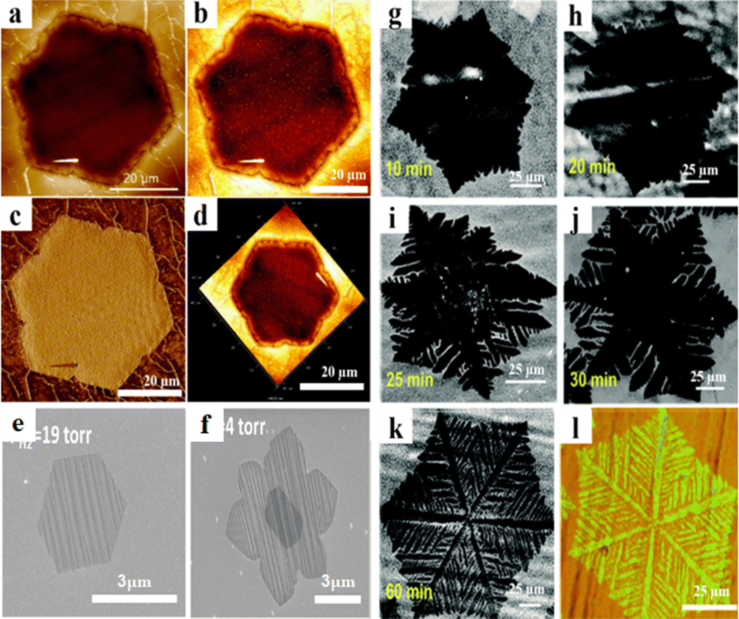 | ||
| Fig. 3 (a)–(d) AFM images of V notched hexagon like-graphene patterns on a liquid Cu/W substrate. Reproduced from ref. 57 with permission from American Chemical Society, copyright 2018. (e) The SEM image shows that perfect hexagon graphene only grows at higher hydrogen pressure. (f) Hexagram-like graphene viewed in the SEM image, grown under low hydrogen pressure. Reproduced from ref. 62 with permission from American Chemical Society, copyright 2011. (g)–(l) SEM images depicting the evolution of dendritic hexagon-like graphene flakes at different times showing a qualitative diagram of the growth and etching pattern. Reproduced from ref. 63 with permission from The Royal Society of Chemistry, copyright 2018. | ||
According to Regmi et al. low H2 pressure during the development of graphene leads to unevenly formed hexagonal grains with low D band intensities.62 Hexagram and perfect regular hexagonal (Fig. 3e and f) shapes were achieved at intermediate low H2 partial pressures and high H2 pressures, respectively. In a 3-inch quartz tube, CVD growth was carried out at room pressure with a total gas flow of 500 sccm (cm3 per min). The partial pressure was attained by the combination of H2 and CH4 in Ar (high purity argon). After heating the Cu foil to 1000 °C in 2.5% H2 in Ar, 0.1% CH4 in Ar was added to start the graphene formation process. H2 has a considerable effect on graphene on Cu; it acts as an art etching agent and an activator of the surface-bound carbon.62 The impact of H2 on CH4 adsorption on Cu foil depends on the ratio of H radicals to CH4 in terms of partial pressure. Regmi et al. were unable to regulate the density of nucleation seeds, due to which it became challenging for them to determine whether or not reduced H2 pressure could result in larger graphene grains.62
Dendritic hexagon-like graphene patterns (Fig. 3g–l) were created on Cu foil using the LPCVD technique by using an in situ increase in H2 flow.63 According to Gebeyhu et al., art etching solely occurred on the unconfined Cu substrate and was absent in the confined copper substrate.63 They highlighted that only in situ hydrogen partial pressure is used during art etching, eliminating the need for external H2. Following 2 minutes of exposure to O2 (1 sccm) on Cu foil, growth was carried out in Ar/H2/CH4 (450/50/1 sccm) for a range of growth durations at 1000 °C,63 with graphene being allowed to develop over a total of 60 minutes. According to Gebeyhu et al., competitive art etching can occur after a specific growth time, or surface-diffusion limited development can result in dendritic graphene.63 Furthermore, the technique used in this research was deemed inadequate, as the nucleation seed density cannot be controlled. As a result, determining whether reduced hydrogen pressure could yield larger graphene grains remained a challenge.63 Comparing the aforementioned publications, they are all found to be based on the same experimental and characterization techniques as well as comparable theoretical frameworks, such as the surface diffusion model, which explains the growth and art etching.57,62,63 Compared to the other two articles, Pham et al.'s paper uses a higher temperature and a greater H2 concentration.57 The authors additionally noted that H radical diffusion at the interface between the liquid Cu and the graphene may be the cause of the art etching.57 The other two employ a set hydrogen partial pressure,62,63 whereas Regmi et al. use a range of H2 partial pressures from 0.01 Torr to 1 Torr.62 They also explain how H2 activation and art etching responsibilities are balanced.62 While the etching is dependent on the increase in H2 partial pressure that occurs naturally as a result of the breakdown of CH4 and the consumption of Cu, Gebeyehu et al. do not add additional hydrogen.63 Additionally, they note that the etching solely affects the unconfined area of Cu.63
Through hydrogen-induced etching, graphene with a zigzag edge evolved into a slanted edge with a hexagonal hole at the center. While using two distinct substrates, Stehle et al. got identical results at 1065 °C for the APCVD technique on either Cu or 10% Cu Ni.64 Separate flows of 500 sccm of 2% H2/Ar and 6 sccm (Cu) or 16 sccm (CuNi) of 0.1% CH4/Ar are added to the chamber, and stopping the flow of CH4 and Ar for a predetermined period of time initiates art etching (5–20 min). Samples were art etched and then placed onto a Si/SiO2 substrate for further characterization.64 Initially, graphene was permitted to grow until it achieved a hexagonal shape with a ZZ edge. Afterwards, the supply of CH4 was stopped while the other parameters remained constant. After that, art etching occurred, resulting in the creation of a hexagon-shaped hole in its center. The edge of the hexagonal hole at the center of the graphene is always parallel to the graphene edge's circumference during the first etching stage. The ZZ edge gives the same hexagonal form to the graphene edge's circumference and hole's edge in the middle.64 The hexagonal hole etching rate is slow when the researchers supply a high concentration of H2, while the etching rate of graphene edge's circumference is fast. In this instance, graphene's circumference underwent a modest transformation, changing from a hexagon with a ZZ edge to a dodecagon (120 °C) with a slanted edge that was 19 °C closer to the ZZ edge (Fig. 4a–h).64 It is noteworthy that within the same sample, the smaller graphene reaches the dodecagon shape (Fig. 4g) more quickly than the larger graphene. Thus, it has been demonstrated that the size of the graphene determines its outer edge shape. According to the kinetic Wulff construction hypothesis, bigger graphene exhibits slower crystal growth along its edge during growth, and faster etching along its circumference during art etching (Fig. 4h), with the hole inside the graphene being erased more slowly.
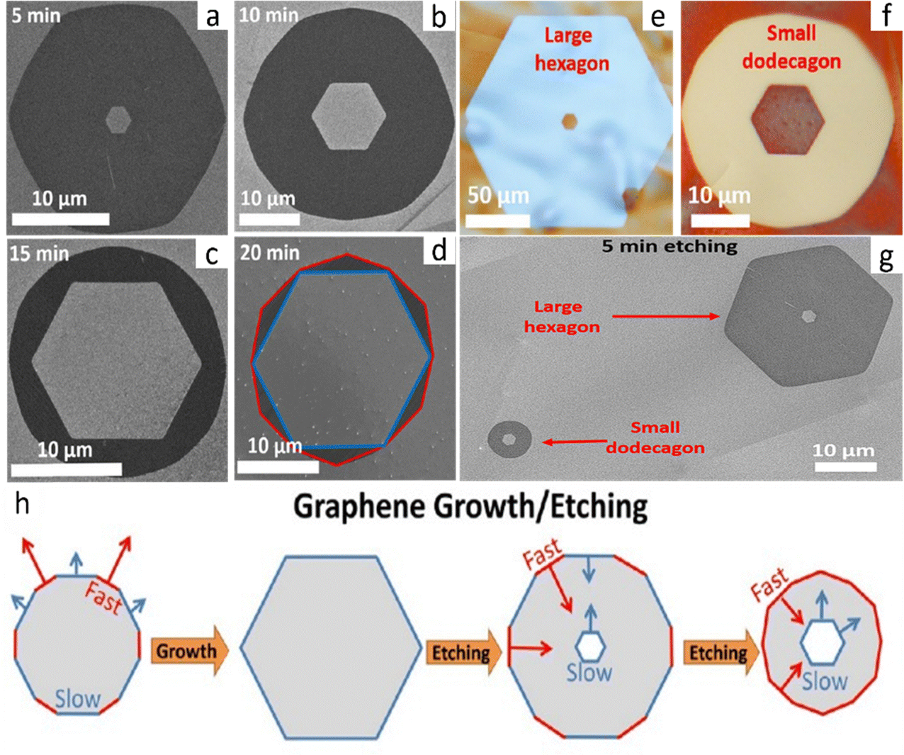 | ||
| Fig. 4 (a)–(g) SEM image of hexagon-in-hexagon and hexagon-in-dodecagon-like graphene etched for different times and hole etching kinetics. (h) Schematic shows graphene growth. During growth, a crystal is terminated by the slowest ZZ edges resulting in a hexagonal shape. Etching exposes the fastest edges on circumference resulting in a dodecagon, while the formed hole is terminated by the slowest ZZ edges. Reproduced with permission from ref. 64. Copyright 2017 American Chemical Society. | ||
2.2. Serrated edge hexagon-like graphene by O2-induced art etching
Grain boundary-free graphene film synthesis using APCVD with O2 concentration adjustment, a straightforward process for producing superior graphene with a flawless hexagonal structure, was described by Guo et al.58 There might be some grain boundaries in the graphene created via CVD. The authors used an O2-assisted CVD art etching system (with O2 and purified H2) in conjunction with a gas purifier that contained potassium hydroxide (KOH) gas to minimize these grain boundaries.58 H2 is cleaned of water contaminants using this gas filter before being transported to the chamber. In this instance, they discovered that when the O2 concentration increases, nucleation density progressively decreases, which will result in grain-bound, grain-steady hexagon graphene (Fig. 5a–c).58 This study discovered that O2 has a significant role in art etching, and an increase in O2 would result in a decrease in the nucleation density, even if the concentration of oxygen (O2 < 0.015%) was lower than that of hydrogen (H2 > 1%).58 O2 was exposed to Cu foil before starting graphene growth and then the conditions utilized for growth are 0.8 sccm of CH4 and 4.5 sccm of H2 and 320 sccm of Ar, in which H2 is from a separate cylinder. O2 and CH4 were both added to the chamber after being diluted in Ar.58 The authors stated that O2 was selected as the oxidizer due to its exact controllability via a mass flow controller. Active areas on the Cu surface are passivated by exposing O species on Cu foil during pre-growth, which significantly limits the nucleation of graphene.58 It has been shown by Guo et al. that O2 will cause the expansion of the graphene domain in addition to suppressing nucleation density.58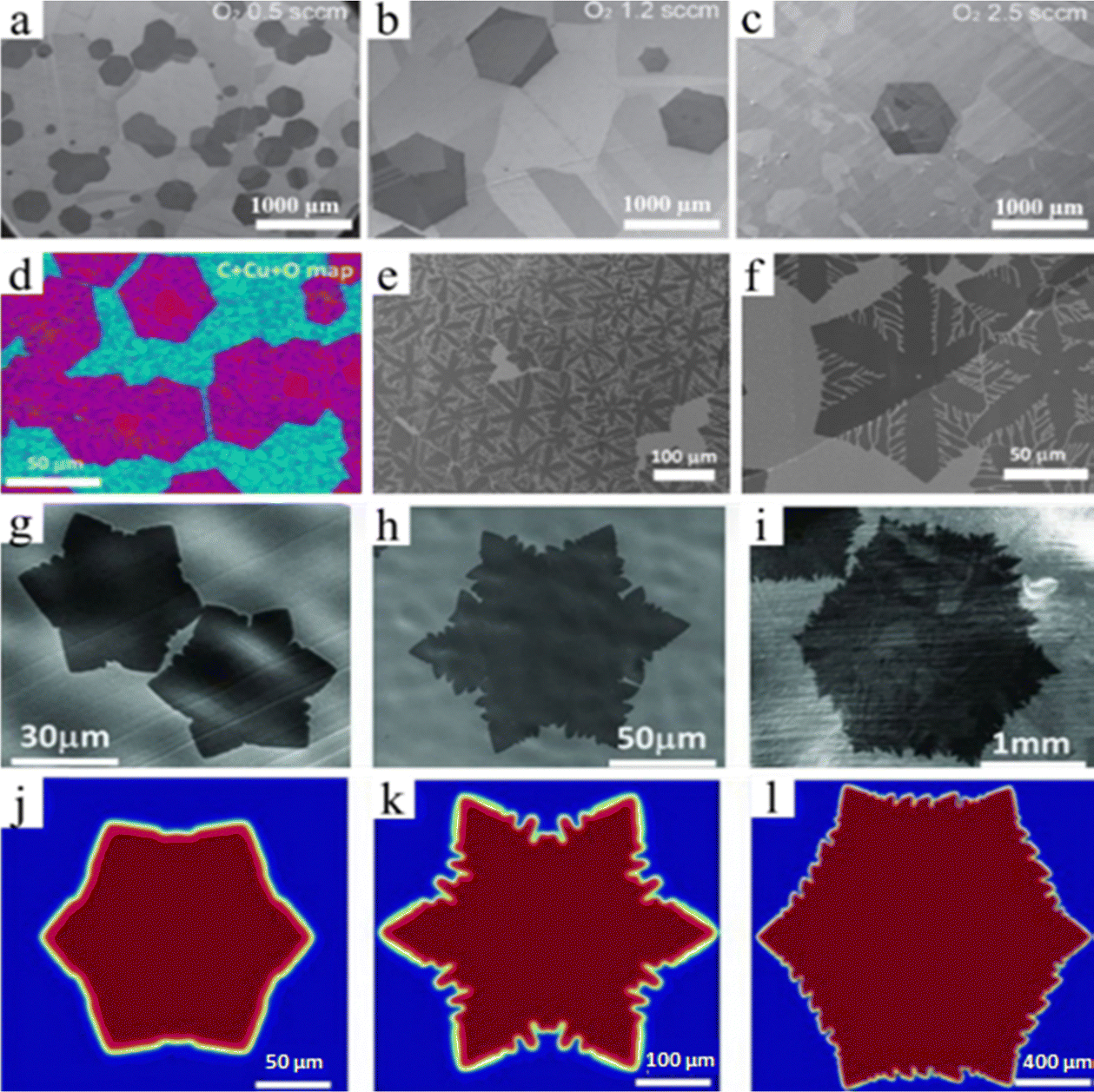 | ||
| Fig. 5 (a)–(c) SEM images of isolated hexagon graphene domains grown on O2 assisted CVD processes under the condition of 0.8 sccm, 4.5 sccm H2 and 320 sccm Ar at 1040 °C. Reproduced from ref. 58 with permission from American Association for the Advancement of Science, copyright 2013. (d)–(f) SEM image of circle-in-hexagon-like and dendritic hexagon-like graphene grown on NR foil by regulating oxygen pressure. Reproduced from ref. 62 with permission from Elsevier, copyright 2013. (g)–(i) SEM image of hexagon-like graphene and serrated edge hexagon-like graphene grown on OF-Cu(O). (j)–(l) Phase field simulation results as a function of characteristic attachment time and C flux. Reproduced from ref. 65 with permission from American Association for the Advancement of Science, copyright 2013. | ||
The art etched graphene that is produced by the researchers is hexagon-shaped and grows on an oxygen-free copper substrate (OF-Cu).62 Nevertheless, dendritic patterned graphene (Fig. 5d–f) is produced when the substrate (OF-Cu(O)) is exposed to O2 and placed within the CVD chamber.62 Clean copper substrates are particularly crucial for art etching, according to Vlassiouk et al.65 In order to clean the substrate in this study, the authors used O2, which passivates the Cu foil and forms an active site and prior to beginning growth and etching, they prepared clean copper. The production process leaves residues on the surfaces of commercially purchased Cu foils. To eliminate these residues, the Cu foil is electropolished, which is then utilized to generate and art etch graphene.65 In contrast to the bare Cu surface, no oxygen was present in the graphene-covered area during the formation of graphene. According to auger electron spectroscopy (AES), this suggests that graphene has extremely effective corrosion resistance. When graphene is exposed to air at a higher temperature, art etching occurs at the interdomain boundaries and forms a pattern like a serrated edge hexagon (Fig. 5g–l).65 Uncertainty surrounds the mechanics of the produced pattern; wrinkles or ripples on graphene could be the source. Compared to earlier obtained etching patterns by using nanoparticles, which featured hexagon-shaped holes and zigzag lines, this etching pattern is distinct.62
2.3. Hexagon-in-dodecagon-like graphene via CH4/H2-induced art etching
The process known as growth–etching–regrowth (G–E–Re) involves the growth, etching, and subsequent regeneration of graphene. This method yields graphene of excellent quality and free of defects. Ma et al. described using the G–E–Re approach to control the ZZ/armchair edge structure during CVD graphene growth on the platinum (Pt) substrate (Fig. 6a–l).66 This resulted in the development of a graphene geometry resembling a hexagon inside a dodecagon (Fig. 6e). Prior to adding a gas mixture of CH4 (3.7 sccm) and H2 (700 sccm) for the graphene growth, they initially formed graphene on the Pt substrate. Following the development stage of graphene, the flow of CH4 was reduced to 3.3 sccm for art etching, while the remaining gas parameters stayed unchanged. This resulted in art etching on the grain boundaries. For graphene regeneration, the CH4 flow was increased from 3.3 to 3.5 sccm after art etching, but all other parameters remained the same.66 First, graphene developed in a regular hexagon shape. Subsequently, the edges or boundaries of graphene began to etch due to the reduced rate of CH4 flow, resulting in the production of slanted edges at the vertex of ZZ-edged hexagon graphene. A dodecagonal shape was formed as the slanted edges continued to migrate inward toward the AC direction (Fig. 6a–c). Upon extending further the etching time, the graphene edge becomes armchair-shaped, creating an angle of approximately 19° from the ZZ edge (120°). Additionally, the density of graphene domains decreased as the etching time increased. The graphene edge was then affected by increasing the CH4 ratio from 3.3 to 3.5 sccm to stimulate regrowth. The ZZ edge marginally alters the dodecagon edge. The flawless hexagon hole was created inside the graphene domain during the art etching stage and did not change shape at that time.66 However, because of the increased rate of CH4, the hexagon hole gradually changed from the ZZ edge to the armchair edge during the regrowth stage. Two edge formations occurred during the evolution of the structure: the armchair edge and the zigzag edge. The armchair edge becomes slanted edge during the progression. The concentration of kinks has a linear relationship with the slanted edge growth/art etching rate.66 The processes of art etching and regeneration are interdependent. On the other hand, the tilted armchair edge structure is dodecagonal while the ZZ edged construction is hexagonal (Fig. 6e). The expansion of the graphene's outer circumference is proportional to the growth of the hole's edge within the material, and vice versa. As a result, the growth and art etching processes always affect the hole edge of graphene. In this experiment, H2 dissociation on the Pt surface with a strong catalytic capacity is what causes art etching. Art etching will always begin at the graphene domain's edges. Ma et al. revealed how single crystal graphene can be art etched and its growth is reliant on the edge structure using the kinetic Wulff concentration theory.66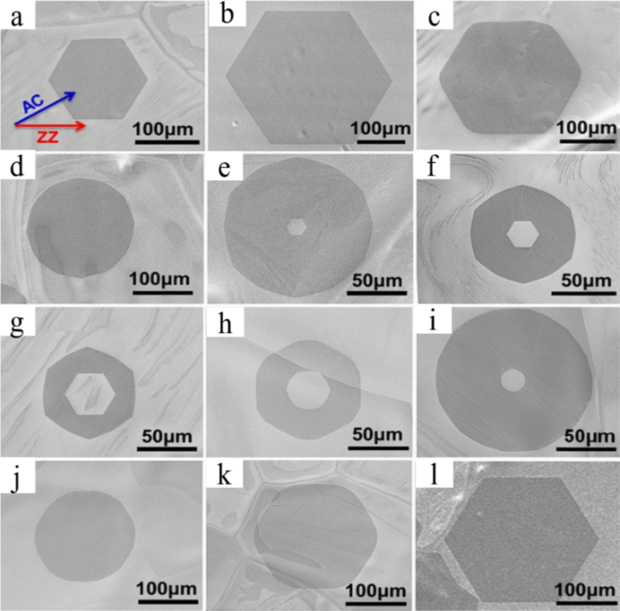 | ||
| Fig. 6 SEM image depicting the evolution of hexagon-in-hexagon-like graphene grown on a Pt surface at various gas flow rates at different times. In all images, the ZZ edge of the graphene domain is oriented along the horizontal direction. (a) and (b) With a gas flow of 700 sccm H2 and 3.7 sccm CH4 with growth times of 15 min and 30 min, (c)–(g) Etching stage: gas flow of 700 sccm H2 and 3.3 sccm CH4 from (b) etched for 4 min, 7 min, 10 min, 11.5 min, 12 min. (h)–(l) The regrowth stage: gas flow of 700 sccm H2 and 3.5 sccm CH4 from (g) for 0.5 min, 2 min, 3 min, 5 min, 9 min. Reproduced from ref. 66 with permission from National Academy of Sciences, copyright 2013. | ||
2.4. Hibiscus flower-like graphene via H2/CH4 gas-induced art etching
By varying the H2 flow rate ratio during the LPCVD graphene development while maintaining a constant CH4 ratio, graphene morphologies evolved from a compact to a dendritic to a fragmented morphology (Fig. 7a–h).60 Cu foil was put into the system, which had been cleaned and subjected to a 200 sccm H2 gas flow. After that, the substrate was heated and annealed for 30 minutes at 1020 °C in a pure H2 atmosphere. To induce graphene to grow on Cu foil, CH4 was introduced into the reactor chamber. Upon the initiation of growth, the H2 flow was adjusted to a precise ratio (15–50 sccm) at a steady pressure. Finally, CH4 was switched off and the system was cooled. Characterization was ultimately performed by bubbling mixed PMMA onto the produced graphene layer.60 Using H2 as an art etching agent to change the shape of the graphene and an activator to promote its growth, Luo et al. discovered that H2 has two functions during the synthesis of graphene.60 At a CH4/H2 rate of 0.5/20 sccm, fragmental star-like graphene (Fig. 7c) appeared on the Cu surface with a high rate of art etching.60 The controlled art etching impact is examined by the researchers by adjusting the CH4/H2 flow ratio further. The researchers discovered that in this instance, the higher H2 flow caused the graphene shape to shift from fragmented to compact. H2 sculpts graphene to grow in a particular shape, according to this paper.60 Increased H2 flow along with CH4 rate will increase the graphene growth and lower the art etching rate.60 Initially, the growth of graphene was fast until reaching a balanced level. When etching and growth are compared, the art etching rate is smaller than the growth rate and increases extremely slowly until it reaches the critical point. The graphene forms that are produced at or close to this critical point have rough edges.60 It should be mentioned that significant art etching will occur and the synthesis of graphene will be suppressed if the H2 flow is increased after reaching this critical stage due to the breakdown of CH4. Additionally, reducing the H2 below the critical point results in an extremely low etching rate, and the formation of graphene would be very slowly controlled leading to the second layer and resulting in a hibiscus flower shape (Fig. 7h).60 Moderate H2 flow is essential in this experiment since these conditions will disrupt the anticipated specific shaped graphene production. The active C atoms are bonded to the Cu surface by H2, which the authors claim act as an activator for CH4. This allows the C atom to diffuse through the Cu surface to reach the graphene edge and grow its layer.60 This allows us to observe that graphene grows near its edge. According to Luo et al. the outcome will always be star-like rather than hexagonal if the hydrogen flow is reduced. This is a result of the high carbon source concentration at the edge.60 When graphene is art etched, the growth process is reversed; carbon in the generated graphene reacts with hydrogen through the copper surface, releasing CH4 as a byproduct. Because the nucleation point has the lowest reaction barrier, first art etching starts there. As hydrogen on graphene continues to flow and diffuse, the further art etching area will grow. Hydrogen diffusion is not constant at the graphene art etched edge, and it will shift in a direction that results in the fractal etching mode. The development of graphene is from fragmented to star-like to fractal.60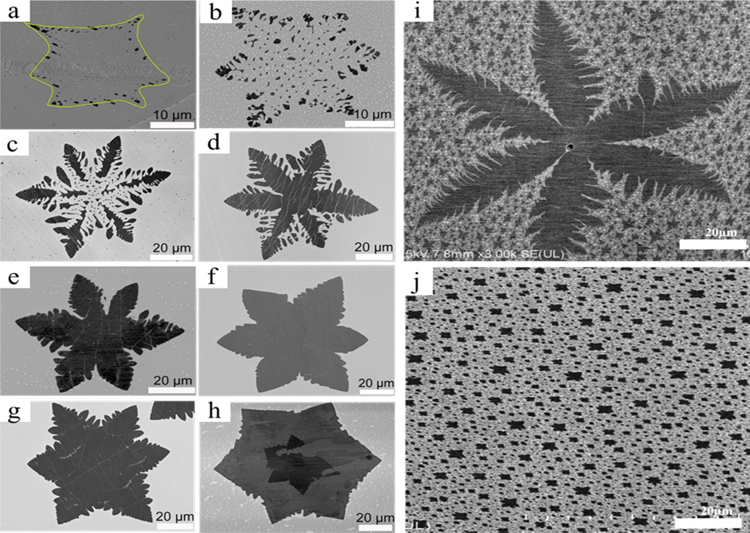 | ||
| Fig. 7 (a)–(h) Magnified SEM images of hibiscus flower-like graphene etching-controlled growth using different CH4/H2 flow rates for 30 min. Reproduced with permission from ref. 60. Copyright 2017 American Chemical Society. (i) SEM micrograph of a snowflake-like graphene growth on a Cu substrate. (j) SEM micrograph of thermal CVD graphene nuclei on copper foil. Reproduced from ref. 67 with permission from IEEE Nanotechnology, copyright 2012. | ||
Creating large domain sized graphene without grain boundaries is essential to fully reap the benefits of graphene.67 Surface diffusion of carbon resulting from H radical etching of graphene and from CH4 or other hydrocarbons on Cu foil leads to the creation of complex networks in graphene domains divided by roughly equal-width alley-like gaps.67 Controlling the dynamic balance point, nucleation, and growth is essential for synthesizing graphene with a unique form and for network alley. Snowflake-like graphene (Fig. 7i and j) formed on Cu foil in the presence of an Ar/H2/CH4 gas mixture at 1000 °C within the CVD furnace. Ar is utilized when a carrier gas is required.67 H2 acts as a growth stimulant and also an etching reagent. CH4 is dissociated by the Cu catalyst during nucleation and growth, releasing carbon, hydrocarbon radicals, and atomic hydrogen.67 Atomic hydrogen produced by Cu catalysts also improves the extraction of atomic hydrogen from methane to allow for the integration of carbon into developing graphene, concentrating solely on the few graphene flakes that are growing in size and preventing any more graphene nucleation.67 In this instance, the graphene shape and combined graphene flakes will be optimized through control of the gas flow. H2-art etched carbon atoms can be recycled to fuel the production of graphene flakes. The giant graphene flake will grow more quickly if other little graphene flakes in the same sample are sacrificed.67 Big graphene flakes are able to expand more quickly than their nearby small counterparts, and their edges are more stable than those of the surrounding graphene flakes.67 According to Tzeng et al., amid a sea of tiny graphene flakes, the art etching, recycling, feeding, and growth processes may produce “huge snow flake-like graphene” (Fig. 7i and j).67 The obtained graphene is of good quality and has minimal edge flaws. Pitfalls leading to a few flaws were found in the obtained graphene, and the authors neglected to describe the etching process.67
2.5. Snowflake-like graphene obtained via Ar/H2 gas-induced art etching
By adjusting the Ar/H2 flow rate ratio during CVD graphene growth, simple Euclidean to snowflake-like (complex fractal) (Fig. 8a–i) designs on a liquid Cu/W substrate may be achieved.59 To successfully etch the produced graphene from the Cu/W substrate in this instance, Ar is used as an inert gas with H2.59 To initiate the nucleation process and establish a channel for the expanded nuclei, a significant amount of energy is needed for both graphene growth and art etching. For the growth and art etching process in this instance, researchers employ high thermal energy at a temperature of 1160 °C.59 At this set temperature, the liquid Cu/W substrate is cleaned by annealing it in pure H2, which also permits CH4 adsorption and diffusion on the substrate surface, hence promoting nucleation in the presence of Ar/H2 as the carrier gas. Following that, CH4 was switched off, and the Ar/H2 flow was kept going for the required amount of time at the same temperature and with a particular flow rate ratio in order to art etch the graphene layer.59 The Ar flow rate ratio (800 sccm) is constantly maintained while the H2 ratio (100, 70, 50, 30, 20, 15, 10, 5, 3 sccm) is reduced. The snowflake-like pattern generated at a ratio of 800/20 sccm is shown in Fig. 8e and the hexagon-like figure art etched pattern acquired at an Ar/H2 ratio of 800/100 sccm is shown in Fig. 8a. The graphene coating was then electrochemically transferred to a 300 nm SiO2/Si substrate for characterization.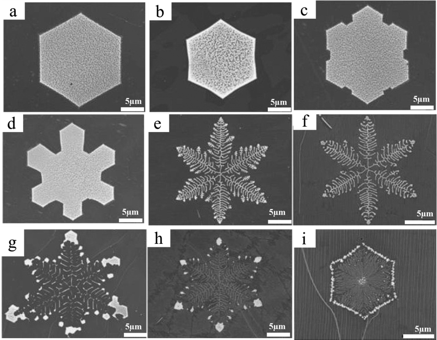 | ||
| Fig. 8 (a)–(i) SEM images of a series of etched hexagons to snowflake-like graphene patterns obtained using various Ar/H2 flow rate ratios at 1160 °C and a growth time of 30 min. Reproduced from ref. 59 with permission from American Chemical Society, copyright 2013. | ||
The findings of Geng et al. indicate that art etching takes place within the graphene film rather than at its border. Additionally, the sluggish art etching rate can be attributed to the low etching agent concentration and hindered surface diffusion between the Cu surface and the graphene film. Rather than commencing their etching simultaneously, various etched graphene patterns on the same sample are generated through distinct steps.59 Researchers looked into how temperature and catalytic type affected this graphene art etching mode and its physical source. Although they substituted a brass substrate for the Cu substrate and altered the temperature range from 1100 °C to 1160 °C, the outcomes were identical to the art etched pattern that was previously achieved.59 Also, they found that when the active art etching agent ratio was less than the Ar ratio on a potential surface, then faster surface diffusion will take place. In this instance, graphene and copper are the two potential surfaces. Liquid Cu is predicted to undergo H2 adsorption and diffusion due to its high surface free energy. In this instance, art etching occurs at the graphene film's rough edge.59 The authors did not provide sufficient explanation of the art etching mechanism to comprehend the art etching approach, nor did they describe how they managed the art etching throughout graphene growth.59
2.6. Nanopores on graphene obtained via a mixture of CH4 and dry gas-induced art etching
Graphene nanopores, tiny holes or pores in a graphene sheet, have been widely studied both theoretically and experimentally because of their potential for application in emerging technologies such as single-ion channels, single-molecule detection, or liquid purification (Fig. 9a–c).68 A theoretical report of Zhang et al. has predicted the significant potential of graphene nanopores for hydrogen storage, achieving approximately 4 mmol g−1 at 300 K and 1 atm.69 Based on evaluation from the perspective of graphene nanopores, Schlichting et al. successfully created graphene membrane nanopores via selective etching.70 Specifically, they used energetic ion irradiation followed by dry, scalable etching in O2 at 1 mbar and 300 °C, selectively enlarging ion-induced defects into larger nanopores. This method allows for independent control of the pore number and size, enabling the optimization of permeance, selectivity and the investigation of separation mechanisms for various pore sizes. In another innovation, Wang et al. have developed a novel technique for producing nanopores on graphene with a tight size distribution and a small tail deviation.71 These nanopores are useful for energy storage, molecule separation, and other electrical device applications. A technique known as cascaded compression, first reported by Wang et al., facilitates the simultaneous creation of new nanopores by compressing the pre-existing ones through gradual shrinkage or expansion.71 The size distribution becomes homogeneous and the density of nanopores increases with each stage. Additionally, several properties of the created nanopores (Fig. 9d) may be independently controlled using this approach. This compression procedure takes place in situ after graphene grows at 1035 °C using the LPCVD technique. The copper foil substrate was positioned over and parallel to the graphite electrode. By altering the electrode structure, the distance (200–2000 μm) between the graphite electrodes may be adjusted. H2 was used to heat the chamber for 24 minutes. After that, the H2 flow was stopped, and one sccm of dry air was injected for one minute to passivate the Cu surface. After that, the Cu foil is exposed to 400 V for 5 minutes while the environment is annealed with H2 (40 scccm). Next, CH4 (0.3) was injected to initiate the formation of graphene with no voltage applied between the electrodes. After 15 minutes, dry air (0–0.3 sccm) was supplied and CH4 was lowered to 0.1 sccm in order to provide an environment of exponential shrinkage for the production of nanopores. E-beam evaporation or in situ electrochemical deposition are two methods that may be used to load the Cu particles onto the graphite electrode. The copper substrate receives an applied negative voltage. As a result, the Cu particles on the graphite electrode ionize, accelerate, and force the carbon atoms in the developing graphene lattice to sputter towards the substrate. On graphene, this sputtering produces nanopores (400 V applied to make a nanopore), and the diametric expansion rate during sputter etching remains constant. In the presence of CH4, graphene grows and the nanopores naturally contract when the electric field is removed. which is controlled by a high adsorption energy barrier.71 The adsorption of the carbon source on the growth substrate is thought to be the limiting step for nanopore shrinking controlled by a high adsorption energy barrier because of the quick surface diffusion of the carbon source and the tiny size of nanopores. This compression method compresses the scattered nanopores by combining shrinkage and expansion. Small nanopore diameters and rapid surface diffusion of carbon sources are limited by nanopore shrinkage, which is controlled by a high adsorption energy barrier.71 Because of cascaded compression, the size distribution of graphene nanopores will include pore engineering, which modifies the size or structure of graphene pores. Compression that reduces the size dispersion of nanopores is called cascaded compression.71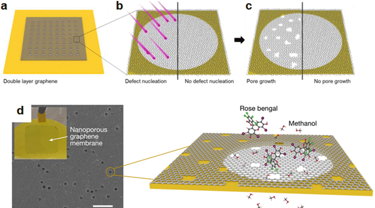 | ||
| Fig. 9 (a) Double layer graphene (DLG) is transferred to porous silicon nitride frame. (b) Energetic ion irradiation introduces defects in a selected area of the DLG membrane. (c) Selective etching in oxygen gas enlarges these defects into pores, while the untouched DLG remains unaffected. Reproduced with permission from ref. 68. Copyright 2020 American Chemical Society. (d) SEM image of nanoporous graphene transferred onto a PITEM (20 nm nominal pore size). Inset, photograph of the nano porous graphene membrane. Scale bar, 200 nm, schematic showing the size-based nanofiltration of Rose Bengal across nanoporous graphene membranes in methanol. Reproduced with permission from ref. 71. Copyight 2023, Nature Publishing Group. | ||
3. Possible mechanisms behind the art etching
The mechanism underlying the combined growth and art etching of graphene remains unclear. However, there are various indications and presumptions that provide insights into how graphene is produced art etched through regulation of growth parameters, circumstances of atmospheric pressure, and gas precursors. Carbon sources stimulate the formation of graphene in CVD processes. Subsequently, an art etching agent is introduced into the chamber, such as H2, CH4, O2, Ar, etc. to art etch the incorrect arrangement of carbon species in their structure (carbon clusters, amorphous carbon, etc.). Etching can occur as a result of precursor gas diffusion across the surface, which happens when the gas reacts with the substrate surface and passes through it. The reactive species will then exit the CVD chamber after reacting to the precursor gas. This thorough analysis revealed a distinct mechanism employing distinct gases (Fig. 10). There are two potential causes of H2 induced art etching: one is that hydrogen will react at the edge where C atoms diffuse through the substrate, and the other is that ambient hydrogen may etch graphene at random.57 CH4 causes H radicals to adsorb, diffuse, and dissociate during CH4-induced art etching. In this instance, the carbon source's dissociated H radicals will diffuse onto the substrate.72 Then in O2 aided art etching, oxygen will help to control the nucleation density of graphene. When oxygen comes into contact with the substrate, it adsorbs and diffuses onto its surface. Moreover, it generates an oxide layer through reaction with the catalyst substrate. Subsequently, the precursor gas introduced into the CVD chamber for the development of graphene will experience H radical adsorption, diffusion, and dissociation. After reacting with O2 to create a hydrocarbon, dissociated H radicals will exit the CVD chamber. Maintaining the necessary amount of precursor or reactant is crucial to getting an excellent art etched pattern and preventing excess etching. Temperature and time also play a significant role in this process. Despite discovering methods for growing and art etching graphene, researchers are currently unable to implement these techniques for large-scale production because of the material's high cost and low quality. Furthermore, we must comprehend the growth kinetics of graphene beforehand to properly comprehend the mechanism underlying a particular art etched design.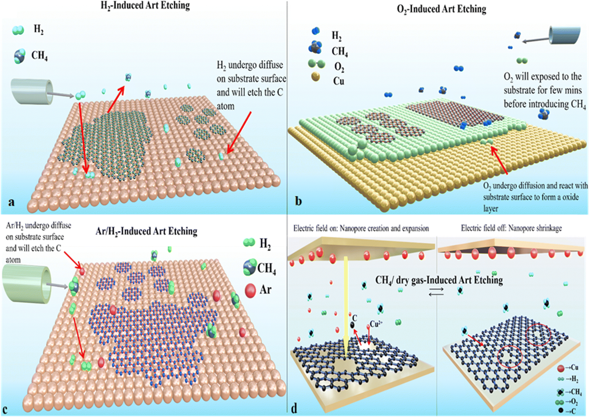 | ||
| Fig. 10 Visual diagram showing etching graphene using different gases during the CVD growth process: (a) H2-induced art etching, (b) O2-induced art etching, (c) CH4-induced etching, and (d) CH4/dry gas-induced art etching. | ||
3.1. H2-induced art etching
It is believed that etching occurs in graphene's defective regions or that art etching nuclei may form at grain boundaries. Pham et al. were insistent that the etched pattern might have resulted from hydrogen diffusion at the interface between the graphene and liquid Cu patterns.57 The increased etching rate was caused by a high concentration of H2 and impaired diffusion at the graphene–liquid copper interface (Fig. 11a).57 The H2 diffusion on isotropic liquid Cu and the physical source of the high symmetry of the art etched Cu pattern may be related. Diffusion etching with varying parameters was also documented in earlier publications. Additionally, nanoparticle etching73 differs from diffusion art etching. When the copper surface is confined, it is separated from the environment and is subject to certain limitations; when the copper surface is unconfined, it is not subject to any constraints.63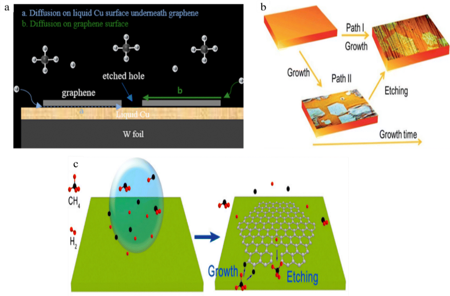 | ||
| Fig. 11 (a) Mechanism of etched Cu patterns embedded into the large-area graphene film with diffusion of etchants underneath and above the liquid Cu surface, which could be mostly responsible for the formation of notched hexagon-like graphene pattern. Reproduced from ref. 57 with permission from American Chemical Society, copyright 2018. (b) Diagram showing the two possible pathways leading to the dendritic hexagon-like graphene pattern. Reproduced from ref. 63 with permission from Royal Society of Chemical, copyright 2018. (c) Schematic illustration showing the process of etching controlled growth during CVD of hibiscus flower-like graphene in H2 diluted CH4. Reproduced from ref. 51 with permission from American Chemical Society, copyright 2017. | ||
Only the unconfined areas of the copper surface experience dendritic art etching of graphene, whereas graphene formed in confined copper surfaces do not experience art etching.63 Using the diffusion art etching, Luo et al. obtained an evolution of art etching-controlled graphene from compact to star and hibiscus shapes using the varied H2 flow rate while keeping the CH4 flow rate constant (Fig. 11c).60 The authors verified that a high H2 flow will halt art etching and progressively speed up development. Low H2 concentrations cause the growth to progressively slow down and the art etching to sharply increase. The authors construct a phase-field model to investigate the growth and art etching mechanisms.60 This simulation demonstrates how crucial it is to regulate the CH4 concentration and the rate of precursor flux onto the Cu surface in order to regulate the growth dynamics of graphene.60
3.2. O2-assisted art etching
It is possible to achieve graphene with low level nucleation density for the centimeter-scale domain by adjusting the O2 concentration and maintaining the appropriate proportions of O2/CH4 and O2/H2. A mass flow controller allows for precise regulation of O2.58 Uncertain amounts of H2O vapor impurities clean the H2 gas in commercially obtained H2. Guo et al. installed a gas purifier in the CVD (Fig. 12a) system and used a flow controller to regulate the O2 concentration. Three distinct CVD systems, O2-free (without H2O purified), O2-free CVD, and O2-assisted CVD, were used by the authors to synthesise graphene. The reaction chamber receives a direct flow of CH4 and H2 gas mixed with balanced Ar gas in the atmospheric pressure CVD system.58 The O2-free CVD system (H2O) will experience fluctuations in nucleation density due to an uncertain quantity of H2O vapor impurities. In contrast, graphene development in O2-free and O2-assisted CVD is stable, and nucleation density gradually decreases as the O2 concentration increases (Fig. 12b and c).58 The nucleation density of graphene increases in the absence of oxidants in the reaction atmosphere and reduces when there is an excess of O2.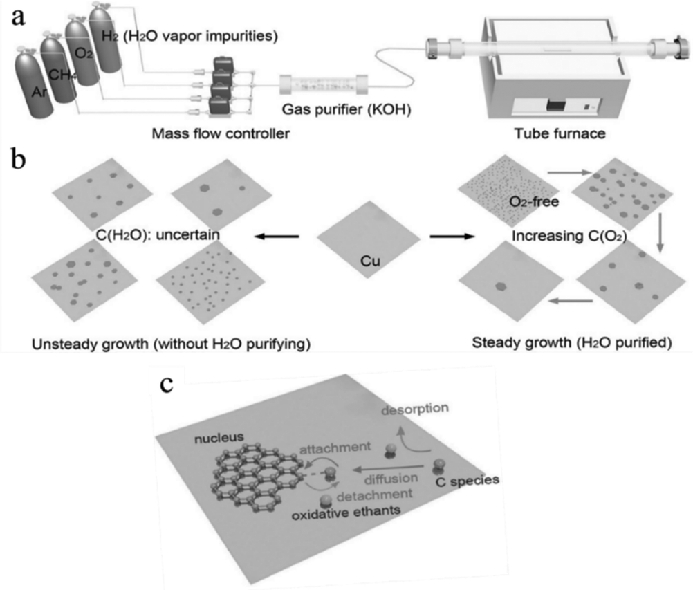 | ||
| Fig. 12 (a) Drawing of the improved CVD system. A tube filled with potassium hydroxide (KOH) as the gas purifier is installed between the reacting chamber and mass flow controllers. The majority of the H2O vapor impurities can be absorbed through the purifier. (b) Illustration of grown hexagon graphene from different CVD processes. C (H2O) and C (O2) represents the concentration of H2O vapor impurities and introduced O2, respectively. (c) Schematic of the pathways of the C species on the surface of Cu during graphene grown in the presence of oxidative etchants. Reproduced from ref. 58 with permission from American Association for the Advancement of Science, copyright 2013. | ||
It should be highlighted that the concentration of H2 is significantly higher than that of O2. At high temperatures, an O2 and H2 combustion reaction will produce H2O steam. In the graphene domain generated by O2-assisted CVD, Cu is oxidized by O2 and H2O vapor, which also facilitates the growth and art etching. When the concentration of O2 was increased while maintaining the same other parameters, etched lines and holes emerged. According to conventional wisdom, the adsorption and breakdown of CH4 will cause Cu to diffuse, which will then lead to the formation of first stable nuclei.
3.3. Ar/H2-induced art etching
For the etchants on the liquid Cu surface to initiate a successful etching process, diffusion is a pre-requisite. Due to its increased surface free energy, the liquid Cu substrate facilitates the absorption or diffusion of the active etchant.59 Geng et al. observed that etching first occurred at the rough edge of graphene and then expanded into a line structure within the graphene region if the Ar concentration was high (Fig. 13).59 However, as seen in Fig. 8a–i, etched patterns begin at the graphene film's center and develop into fractal patterns. The length of the edge-initiated etching is clearly exhibited with different rates more than the center-initiated etching. The diffusion of H2 and H atoms is considered as the efficient etchant in these two circumstances.59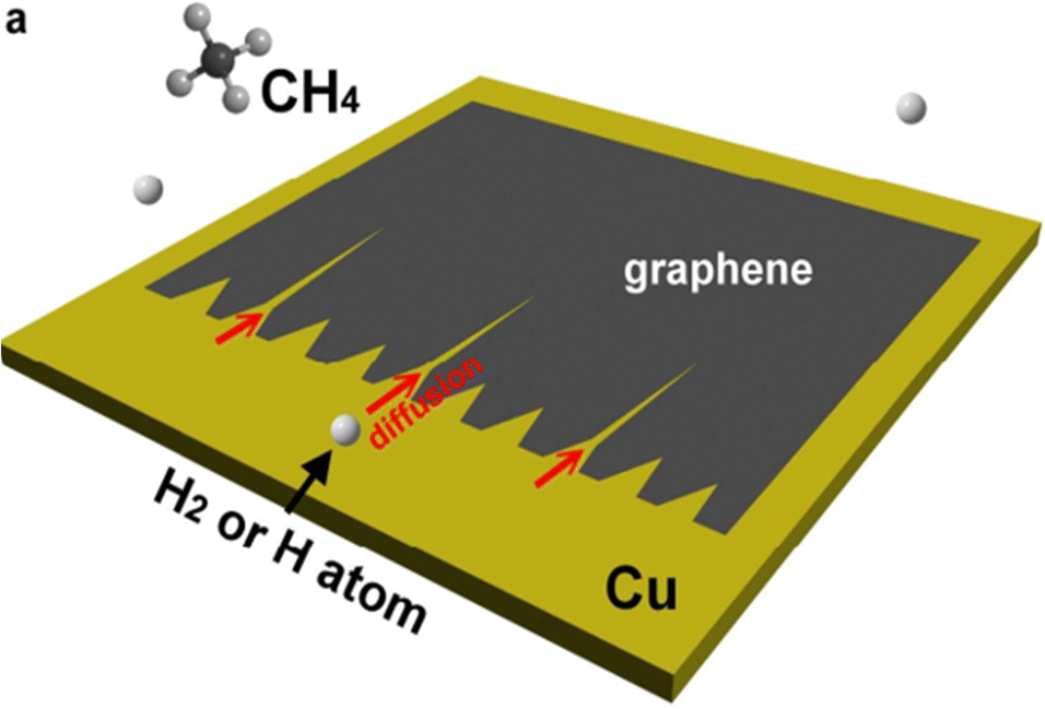 | ||
| Fig. 13 (a) Schematic of the possible mechanism of snowflake-like graphene etching, it is from the boundaries of the graphene film and etching within the graphene film. Reproduced from ref. 59 American Chemical Society, copyright 2013. | ||
3.4. CH4 and dry-gas induced art etching
During the LPCVD graphene development, sputter etching of nanopores via cascaded out in situ. In situ electrochemical deposition and e-beam evaporation are two methods used by researchers to load Cu particles onto graphite electrodes in order to produce sputtering.71 When a negative voltage is applied to a copper substrate, ionized, accelerated Cu particles on the graphite electrode strike the substrate, causing carbon atoms from the developing graphene lattice to sputter (Fig. 14).71 On graphene, sputtering caused nanopores to develop, and sputter etching causes the diameter compression is carried of the nanopores to continuously increase. When there is no electric field, the nanopores shrink, but the graphene continues to expand when CH4 is present.71 Because of the small nanopores and the rapid surface diffusion of the carbon source, the adsorption of the carbon source on the growth substrate is restricted for nanopore shrinking by a high adsorption energy barrier.71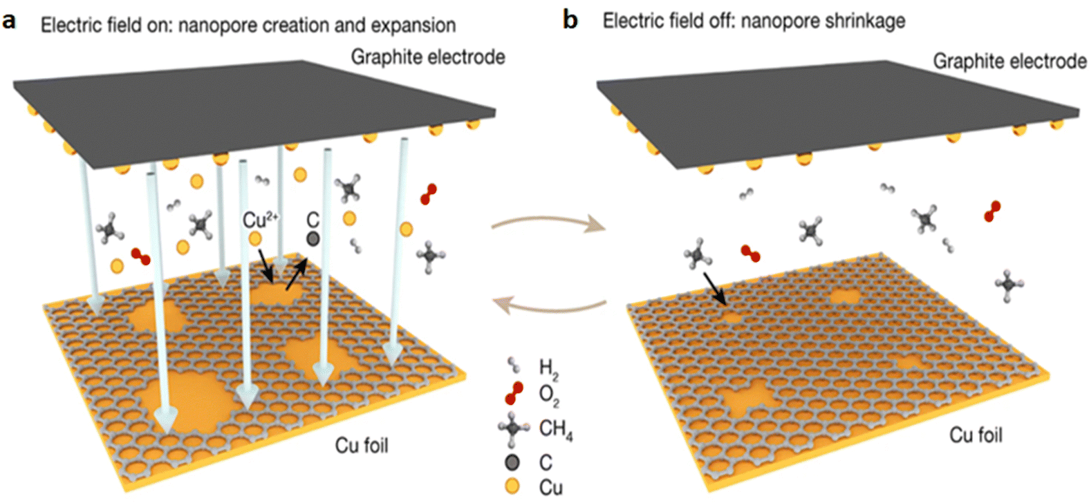 | ||
| Fig. 14 (a) Creation and expansion of nanopores by an in situ Cu sputter, (b) shrinkage of nanopores by regrowth. Reproduced from ref. 71, Springer Nature, copyright 2023. | ||
4. Summary and what is the next path of the art etching?
The graphene geometries were skillfully sculpted into a variety of Euclidean and non-Euclidean forms using these art etching techniques. To improve the understanding of the fundamental principles behind the regulated process of art etching development, an in depth understanding of graphene art etching is essential. In previous years, researchers have described the principles behind graphene art etching, resulting in the realization that the art etching can begin concurrently during CVD at the edge or at the core of the developing graphene. Chemical etching, or CVD, is a method that was first used in the early 1970s to etch graphene in order to create a surface microstructure. These microstructures aid in the creation of more intricate electronic devices and have opened up the way for the development of other specialized etching techniques, such as atomic layer etching (ALD), which aids in atomic-level etching control. For instance, Simonet et al. have successfully achieved graphene nanoribbons via the etching process in O2 plasma.74 This method is a gentle and controlled process and can minimize damage, preserving the intrinsic properties of graphene.75 ALD can potentially create high aspect ratio nanopores with smooth sidewalls, which is advantageous for applications like filtration and sensing where a precise pore geometry is essential. Therefore, ALD-produced art etched graphene is necessary for the creation of nanoscale electronics. However, to achieve special geometries of graphene such as nonporous graphene or snowflake graphene, the ALD strategy has still not yet been widely applied, due to these structures requiring extremely precise and uniform patterning at the nanoscale; besides, ALD may struggle with the consistency and complexity required for such intricate designs, especially over larger areas. Additionally, integrating ALD into these workflows can be challenging, and it might require different conditions (e.g., temperatures and gases) that are not easily compatible with the existing graphene fabrication process. To date, scientists still mainly focus on enhanced CVD techniques for art etching, which is an essential component of microfabrication procedures and micro-electro-mechanical systems (MEMS). Currently, researchers are investigating viable solutions to improve the regulation and functionalities of CVD.27 The art etched/grown graphene achieved through the innovative CVD integrated growth/etching process represents a promising advancement in the field of graphene fabrication. This method combines the strengths of chemical vapor deposition for controlled growth with the simultaneous etching, allowing for the creation of intricated patterns and structures with a high degree of precision. The controlled art etching during growth opens up new possibilities for tailoring graphene-based materials for diverse applications, ranging from electronics to sensors. The integrated growth/art etching process not only enhances the efficiency of graphene production but also provides a platform for designing custom patterns that meet specific functional requirements. This approach holds great potential for the development of advanced materials with tailored properties, paving the way for achieving breakthroughs in various technological domains. As research continues in this area, addressing scalability and reproducibility and further optimizing the growth/etching parameters will be crucial for translating these advancements into practical applications on an industrial scale.Additionally, exploring new art etching agents and expanding the scope of potential applications will contribute to unlocking the full potential of art etched-grown graphene. It also plays a pivotal role in generating nanostructures on the graphene surface, a crucial aspect for the functionality of various nanodevices, nanosensors,76,77 nanofilters and other possible applications are illustrated in Fig. 15. For instance, Wang et al. have published in 2021 about potential graphene nanopores for application in water desalination using artificial intelligence.78 Although the created optimal graphene nanopores exhibited a lower water flux compared with normally circular pores with the same area, they showed a much higher ion rejection rate, approximately about 90%. This is because the enhanced water evaporation has been reported for nanochannels where evaporation occurs through a slit or an extended air–water interface at the nanochannel edge.79 The evaluated immense potential of graphene nanopores for water desalination application is extremely promising to apply in reality. Another investigation of nanoporous graphene also revealed a uniform electronic band gap and rationally engineered emergent electronic properties, which are promising for its application in electronic devices. Therefore, Mutlu et al. have prepared nanoporous graphene for application in transistors via bottom-up synthesis with an excellent switching behavior with on–off ratios exceeding 104, which make them potentially promising for logic applications.80 Research, exemplified by Wang et al., has identified graphene nanopores as particularly suitable for fabricating ultrafast nanofilters.71 Through the precise sculpting of graphene structures, scientists can finely adjust the electrical, mechanical and chemical properties of graphene. It shows that scientists are able to precisely control the electrical, mechanical, and chemical properties of graphene by carefully shaping its configurations. Graphene has a high surface-to-volume ratio, which is remarkable. The art etching process plays a major role in revealing the reactivity of graphene. Because of its increased reactivity, graphene is better able to interact with particular gases and compounds. These adaptable qualities are useful in gas sensors that are intended to identify compounds such as oxygen,76 and ammonia.77 Therefore, the complex art etching technique improves graphene's performance and versatility in a range of technological applications. In this comprehensive review, the art etching and its possible mechanism using various gases and several promising applications of art etching of graphene have been discussed. At first, six types of graphene art etching techniques using various gases during the CVD process have been reviewed and the general mechanism of these techniques is also discussed. Art etching strategies, parameters and structure names are shown in Table 1. In all of the types, H2 plays a key role in art etching of graphene but still each sub-section in this comprehensive review is classified by different gas parameters and different etching techniques. H2-induced art etching is carried out at high H2 concentration and also with in situ increase of H2 partial pressure. O2-induced art etching helps to control the graphene nucleation sites by exposing low concentration O2 to the substrate surface to form an oxide layer on the substrate. Furthermore, the art etching will take place by H2 diffusion on the oxide substrate. In the case of CH4-induced art etching the CH4 flow was decreased for art etching and increased for regrowth while H2 was kept constant for the whole process. In the case of H2/CH4-induced art etching, the H2 rate will be set to the critical point and balancing the H2 in the critical point will control the art etching, when the H2 flow is increased over the critical point with constant CH4, then etching will destroy the graphene. If the H2 flow is decreased to below the critical point, then the growth dominates the art etching. H2/Ar-induced art etching is similar to the H2 induced art etching but in this case Ar gas will be continued for the whole process. Ar is a carrier gas which helps preventing unwanted reactions and will keep the temperature constant. CH4/dry gas-induced etching happens due to cascaded compression using two graphite electrodes.
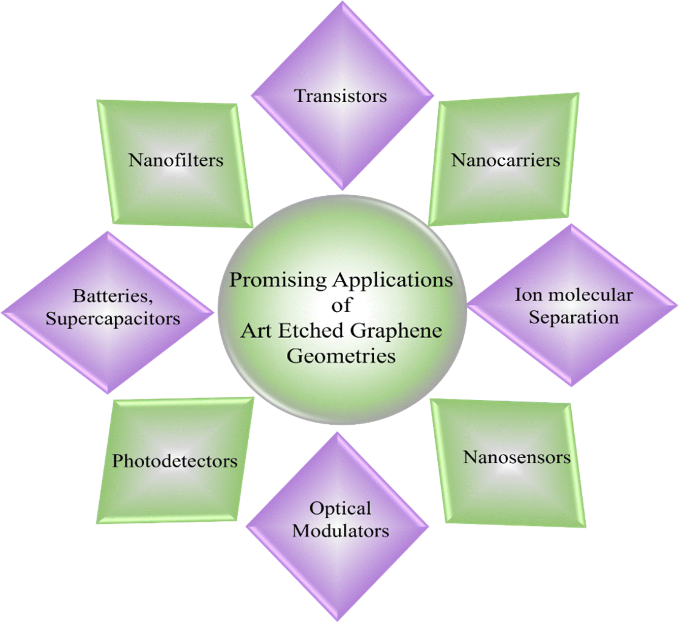 | ||
| Fig. 15 Promising applications of the Euclidean and non-Euclidean art etching of graphene geometries through the CVD process. | ||
| Materials | Art etching strategies | Structure/pattern | Art etching parameters | Applications | Ref. |
|---|---|---|---|---|---|
| Liquid Cu/W foil, H2, CH4 | Diffusion of H radicals on the Cu surface with high H2 concentration | Notched hexagon-like graphene | Art etching occurs at 1090 °C for 30 min | NA | 57 |
| Cu foil, H2 | Maintaining an equilibrium of hydrogen pressure between the art etching and growth | Hexagram-like graphene | Art etching occurs at 1000 °C for 30 min | NA | 26 |
| Cu foil, H2, Ar, CH4 | Etching on unconfined copper foil results from a gradual increase in H2in situ. | Dendritic hexagon-like graphene etching | Art etching at 1000 °C for 60 min | NA | 63 |
| Cu foil, Ar, H2, CH4 | Art etching is caused by an increase in the partial pressure of hydrogen in situ. | Hexagon-in-dodecagon-like structure | Art etching occurs at 1065 °C at 5–25 min | NA | 64 |
| Cu foil, H2, Ar, CH4, O2 | Low O2 concentration leads to etching line such as fractal etching | Perfect hexagon graphene | Annealed at 1045 °C for 30 min | NA | 58 |
| Cu foil, H2, O2 | Exposing O2 to substrate surface will helps to control the graphene nucleation | Dendritic-hexagon-like graphene | Annealed at 1000 °C for 60 min | NA | 62 |
| Cu foil, H2, CH4, O2 | In addition to aiding in substrate surface etching, O2 is crucial in altering the shape of graphene | Serrated edge hexagon-like graphene | Annealed at 1035 °C for 30 min in the presence of H2 | NA | 65 |
| Pt foil, H2, CH4 | The only thing that causes growth or etching during the APCVD and G–E–RG processes is a change in the concentration of CH4 | Hexagon-in-hexagon-like graphene | Annealing at 1040 °C for 70 min | NA | 66 |
| Cu foil, CH4, H2 | Regulating H2 flow while fixed CH4 flow induces etching during LPCVD graphene growth | Hibiscus flower-like graphene | Art etching at 1020 °C for 30 min | NA | 60 |
| Cu foil, CH4, Ar, H2 | Etching occurred by changing various Ar/H2 flow rate during APCVD growth | Snowflake-like graphene | Heated at 1160 °C heating for 30 min leads to snowflake-like pattern | NA | 59 |
| Cu foil, H2 CH4, graphite electrodes | Cascaded compression of nanopore distribution by shrinkage and expansion lead to sputter-etching during the LPCVD process | Nanopores on graphene | Art etching occurs at 1035 °C for 24 min | Ultrafast nanofilters | 71 |
Finally, the integrated growth/art etching of graphene by CVD necessitates exact control over a number of vital parameters and quality of the metal catalyst layer. Creating distinct Euclidean and non-Euclidean geometries requires the accuracy of experimental parameters. The integrated art etching/growth method is regarded practical despite its limitations. Notably, hydrogen plays a key role by diffusion, reaction and dissociation in sculpting the graphene and other used gases also contribute significantly to etch the graphene. During CVD, art etching can occur at the graphene domain boundaries or edges, especially in the substrate's unconfined areas because the carbon species at the edge react strongly with etching chemicals, and areas with a large concentration of grains are ideal locations for the nucleation of etching. As such, the combined growth/art etching method using CVD requires naturally unpredictable conditions. So, researchers must carefully adjust a number of CVD growth parameters to guarantee the synthesis of high-quality, defect-free graphene.81,82 It is essential to strike this balance when creating art etchings. Furthermore, a variety of simulation techniques can be used by researchers to clarify issues related to art etching, nucleation density, morphology, and kinetics of graphene formation. These simulation methods provide an initial prediction to obtain Euclidean and non-Euclidean graphene geometries to carry out real investigations.83
What is the next path of the art etching?
The combination of grown and art etched graphene is expected to pave the way for new research directions, especially in the areas of electronics and optoelectronics.84 Particularly, integrating produced and etched graphene with particular patterns has the potential to produce unique circuit layouts in electrical devices.85 In addition to traditional silicon-based catalysts, integrated graphene structures emerge as catalysts for the next wave of 2D electronic devices into a new era of efficiency and performance.86 Beyond electronics, etched graphene's improved conductivity makes it a good fit for energy storage technologies like batteries and supercapacitors. Graphene is a material that shows promise for application in advanced batteries due to its high surface area and conductivity.87 This material may be used to create fast-charging and high-energy-density battery technologies. Additionally, using integrated graphene structures might significantly improve the conductivity and efficiency of fuel cell components. This development may bring about a new age of improved energy utilization and conversion. Its optical characteristics also make it suitable for use in a range of modulators and photodetectors.86,88–94 In the domain of optical modulators, integrated graphene structures present opportunities for achieving significant advancements in photonics.95–97 This innovation holds the potential to reshape communication systems, pushing the boundaries of what is achievable in the realm of optical technology. It is envisaged that advancements in CVD etching methods would yield uniformly patterned, high-quality graphene with perfect characteristics that may be used in biosensors and filters. The strategic integration of graphene, adorned with specific patterns or modifications, paves the way for highly sensitive biosensors.98 This breakthrough technology promises transformative contributions to medical diagnostics by enabling the precise detection of biomolecules.99 Embracing membrane technology, etched graphene membranes redefine water filters. Capitalizing on graphene's impermeability to most substances, these membranes selectively permit the permeation of water molecules, offering a highly efficient solution for water purification. The construction of in-plane heterostructures with other 2D and 3D materials can be facilitated by the scalability of integrated etched graphene,90,100,101 potentially contributing to the development of quantum computer components. When etched graphene is smoothly incorporated into composite materials, it changes everything by improving the material's overall performance, thermal conductivity, and mechanical strength. Wide-ranging effects result from this discovery, especially in sectors where material performance is critical, like the aerospace and automobile industries. Moore's law permitting, graphene-based transistors could play a key role in expanding the possibilities of conventional silicon-based flexible and wearable technology. Applications such as foldable displays and smart textiles could greatly benefit from the use of art-etched graphene in flexible and transparent electronics.Through manipulating the material's topology by art etching, graphene can have strain and change its electrical band structure due to its inherent curvature. Some unique electrical properties that are absent in flat graphene can be found in this non-Euclidean structure. When compared to a uniform graphene layer, some capabilities cannot be found in state-of-the-art etched graphene due to its unique geometry. Furthermore, high surface area and complex connectivity are two more benefits of art etched graphene that make it potentially useful for applications requiring high adsorption capacity. This art etching effect of 2D materials (e.g. graphene) might unveil a new path for architecturization of 2D surfaces aiming to achieve the light trapping effect for achieving high performance in nanolayers, molecular sensors, etc.102 Especially, dendritic shaped art etched graphene will help in light trapping by its enhanced light absorption, multiple reflection and scattering effect. Also, the existing localized edges were carved into graphene via the zigzag art.
Abbreviations
| CVD | Chemical vapor deposition |
| LPCVD | Low-pressure chemical vapor deposition |
| APCVD | Atmospheric pressure chemical vapor deposition |
| Cu | Copper |
| Ar | Argon |
| H2 | Hydrogen |
| CH4 | Methane |
| Pt | Platinum |
| IBE | Ion beam etching |
| ALE | Atomic layer etching |
| RIE | Reactive ion etching |
| STM | Scanning tunneling microscope |
| SEM | Scanning electron microscope |
| FETs | Field-effect transistors |
| TEM | Transmission electron microscope |
| SAED | Selected area electron diffraction |
| OM | Optical microscopy |
| QDs | Quantum dots |
| 2D | Two-dimensional |
| 3D | Three-dimensional |
| rGO | Reduced graphene oxide |
| GO | Graphene oxide |
| ZZ | Zigzag |
| AC | Armchair |
| ALD | Atomic layer deposition |
| MEMS | Micro-electro-mechanical systems |
| TMDS | Transition metal dichalcogenides |
| TMC | Transition metal chalcogenide |
| EDS | Energy-dispersive X-ray spectroscopy |
| AFM | Atomic force microscopy |
| STEM | Scanning transmission electron microscopy |
| XRD | X-ray diffraction |
| XPS | X-ray photoelectron spectroscopy |
| EDS | Energy-dispersive X-ray spectroscopy |
| FET | Field-effect transistor |
| FE-SEM | Field emission scanning electron microscopy |
| AES | Auger electron spectroscopy |
| Edax | Energy dispersive X-ray analysis |
| PMMA | Polymethyl methacrylate |
| ROS | Reactive oxygen species |
| GNRs | Graphene nanoribbons |
| COL | Collagen |
| PVD | Physical vapor deposition |
Author contributions
G. D. N., T.-H. M.: writing-original draft, writing-review & editing; R. K. G.: review & editing; and P. V. P.: conceptualization, funding acquisition, project administration, supervision, writing-original draft, writing-review & editing.Conflicts of interest
The authors declare no competing financial interest.Acknowledgements
This work is supported by the National Science and Technology Council, Taiwan (Grant No. NSTC-112-2112-M-110-004-MY3).References
- A. K. Geim and K. S. Novoselov, Nat. Mater., 2007, 6, 183–191 CrossRef CAS PubMed.
- V. P. Pham, A. Mishra and G. Young Yeom, RSC Adv., 2017, 7, 16104–16108 RSC.
- S. H. Kim, G. S. Kim, J. K. Kim, J. H. Park, C. Shin, C. Choi and H. Y. Yu, IEEE Electron Device Lett., 2015, 36, 884–886 CAS.
- C. Lee, X. Wei, J. W. Kysar and J. Hone, Science, 2008, 321, 385–388 CrossRef CAS PubMed.
- D. Cohen-Tanugi and J. C. Grossman, Nano Lett., 2014, 14, 6171–6178 CrossRef CAS PubMed.
- U. Stöberl, U. Wurstbauer, W. Wegscheider, D. Weiss and J. Eroms, Appl. Phys. Lett., 2008, 93, 051906 CrossRef.
- I. Y. Lee, H. Y. Park, J. H. Park, G. Yoo, M. H. Lim, J. Park, S. Rathi, W. S. Jung, J. Kim, S. W. Kim, Y. Roh, G. H. Kim and J. H. Park, Nanoscale, 2014, 6, 3830–3836 RSC.
- A. A. Balandin, S. Ghosh, W. Bao, I. Calizo, D. Teweldebrhan, F. Miao and C. N. Lau, Nano Lett., 2008, 8, 902–907 CrossRef CAS PubMed.
- P. V. Pham, R. Soc. Open Sci., 2018, 5, 1–6 Search PubMed.
- P. V. Pham, Nature-Inspired Self-Cleaning Surfaces, Nanotechnol, Era, 2023, p. 120 Search PubMed.
- A. H. Castro Neto, F. Guinea, N. M. R. Peres, K. S. Novoselov and A. K. Geim, Rev. Mod. Phys., 2009, 81, 109–162 CrossRef CAS.
- K. S. Novoselov, A. K. Geim, S. V. Morozov, D. Jiang, Y. Zhang, S. V. Dubonos, I. V. Grigorieva and A. A. Firsov, Science, 2004, 306, 666–669 CrossRef CAS PubMed.
- J. W. Park, J. T. Lim, J. S. Oh, S. H. Kim, P. P. Viet, M. S. Jhon and G. Y. Yeom, J. Vac. Sci. Technol., A, 2013, 31, 031101 CrossRef.
- L. A. Falkovsky, J. Phys.: Conf. Ser., 2008, 129, 012004 CrossRef.
- N. Ghofraniha and C. Conti, J. Opt., 2019, 21, 053001 CrossRef CAS.
- J. Wang, X. Xu, X. Mu, F. Ma and M. Sun, Mater. Today Phys., 2017, 3, 93–117 CrossRef.
- E. Pollmann, A. Maas, D. Marnold, A. Hucht, R. M. Neubieser, M. Stief, L. Madauß and M. Schleberger, 2D Mater., 2022, 9, 035001 CrossRef CAS.
- K. Nassiri Nazif, A. Daus, J. Hong, N. Lee, S. Vaziri, A. Kumar, F. Nitta, M. E. Chen, S. Kananian, R. Islam, K. H. Kim, J. H. Park, A. S. Y. Poon, M. L. Brongersma, E. Pop and K. C. Saraswat, Nat. Commun., 2021, 12, 1–9 CrossRef PubMed.
- A. Cohen, A. Patsha, P. K. Mohapatra, M. Kazes, K. Ranganathan, L. Houben, D. Oron and A. Ismach, ACS Nano, 2021, 15, 526–538 CrossRef CAS PubMed.
- A. Qadir, T. K. Le, M. Malik, K. Aniya, A. Min-Dianey, I. Saeed, Y. Yu, J. R. Choi and P. VPham, RSC Adv., 2021, 11, 23860–23880 RSC.
- K. Celebi, M. T. Cole, J. W. Choi, F. Wyczisk, P. Legagneux, N. Rupesinghe, J. Robertson, K. B. K. Teo and H. G. Park, Nano Lett., 2013, 13, 967–974 CrossRef CAS PubMed.
- V. P. Pham, K. N. Kim, M. H. Jeon, K. S. Kim and G. Y. Yeom, Nanoscale, 2014, 6, 15301–15308 RSC.
- V. P. Pham and G. Y. Yeom, Adv. Mater., 2016, 28, 9024–9059 CrossRef CAS PubMed.
- J. Shim, H. S. Kim, Y. S. Shim, D. H. Kang, H. Y. Park, J. Lee, J. Jeon, S. J. Jung, Y. J. Song, W. S. Jung, J. Lee, S. Park, J. Kim, S. Lee, Y. H. Kim and J. H. Park, Adv. Mater., 2016, 28, 5293–5299 CrossRef CAS PubMed.
- G. Nandamuri, S. Roumimov and R. Solanki, Nanotechnology, 2010, 21, 145604 CrossRef CAS PubMed.
- I. Vlassiouk, M. Regmi, P. Fulvio, S. Dai, P. Datskos, G. Eres and S. Smirnov, ACS Nano, 2011, 5, 6069–6076 CrossRef CAS PubMed.
- P. V. Pham, Chem. Vap. Depos. Nanotechnol., 2019, 42–48 Search PubMed.
- V. P. Pham, M. T. Nguyen, J. W. Park, S. S. Kwak, D. H. T. Nguyen, M. K. Mun, H. D. Phan, D. S. Kim, K. H. Kim, N. E. Lee and G. Y. Yeom, 2D Mater., 2017, 4, 025049 CrossRef.
- Y. Xu, H. Cao, Y. Xue, B. Li and W. Cai, Nanomaterials, 2018, 8, 942 CrossRef PubMed.
- R. Narayan and S. O. Kim, Nano Converge., 2015, 2, 20 CrossRef PubMed.
- Z. Li, R. J. Young, C. Backes, W. Zhao, X. Zhang, A. A. Zhukov, E. Tillotson, A. P. Conlan, F. Ding, S. J. Haigh, K. S. Novoselov and J. N. Coleman, ACS Nano, 2020, 14, 10976–10985 CrossRef CAS PubMed.
- T. K. Le, P. V. Pham, C. L. Dong, N. Bahlawane, D. Vernardou, I. Mjejri, A. Rougier and S. W. Kim, J. Mater. Chem. C, 2022, 10, 4019–4071 RSC.
- T. O. Terasawa and K. Saiki, Carbon N. Y., 2012, 50, 869–874 CrossRef CAS.
- Z. Bo, Y. Yang, J. Chen, K. Yu, J. Yan and K. Cen, Nanoscale, 2013, 5, 5180–5204 RSC.
- V. P. Pham, Y. W. Jo, J. S. Oh, S. M. Kim, J. W. Park, S. H. Kim, M. S. Jhon and G. Y. Yeom, Jpn. J. Appl. Phys., 2013, 52, 075102 CrossRef.
- V. P. Pham, K. H. Kim, M. H. Jeon, S. H. Lee, K. N. Kim and G. Y. Yeom, Carbon N. Y., 2015, 95, 664–671 CrossRef CAS.
- L. Sun, B. Chen, W. Wang, Y. Li, X. Zeng, H. Liu, Y. Liang, Z. Zhao, A. Cai, R. Zhang, Y. Zhu, Y. Wang, Y. Song, Q. Ding, X. Gao, H. Peng, Z. Li, L. Lin and Z. Liu, ACS Nano, 2022, 16, 285–294 CrossRef CAS PubMed.
- P. V. Pham, Atmospheric Pressure Chemical Vapor Deposition of Graphene, IntechOpen, 2019.
- M. C. Lemme, D. C. Bell, J. R. Williams, L. A. Stern, B. W. H. Baugher, P. Jarillo-Herrero and C. M. Marcus, ACS Nano, 2009, 3, 2674–2676 CrossRef CAS PubMed.
- W. S. Lim, Y. Y. Kim, H. Kim, S. Jang, N. Kwon, B. J. Park, J. H. Ahn, I. Chung, B. H. Hong and G. Y. Yeom, Carbon N. Y., 2012, 50, 429–435 CrossRef CAS.
- A. Dey, A. Chroneos, N. S. J. Braithwaite, R. P. Gandhiraman and S. Krishnamurthy, Appl. Phys. Rev., 2016, 3, 021301 Search PubMed.
- K. C. Yang, S. W. Park, M. H. Jeon, V. P. Pham, D. Y. Lee, T. H. Shim, J. G. Park and G. Y. Yeom, Vacuum, 2016, 127, 82–87 CrossRef CAS.
- S. Kondo, H. Kondo, Y. Miyawaki, H. Sasaki, H. Kano, M. Hiramatsu and M. Hori, Jpn. J. Appl. Phys., 2011, 50, 075101 CrossRef.
- D. Bischoff, T. Krähenmann, S. Dröscher, M. A. Gruner, C. Barraud, T. Ihn and K. Ensslin, Appl. Phys. Lett., 2012, 101, 203103 CrossRef.
- R. Ye, D. K. James and J. M. Tour, Acc. Chem. Res., 2018, 51, 1609–1620 CrossRef CAS PubMed.
- R. Ye, D. K. James and J. M. Tour, Adv. Mater., 2019, 31, 1803621 CrossRef PubMed.
- K. G. Libbrecht, Rep. Prog. Phys., 2005, 68, 855–895 CrossRef.
- X. Wang and H. Dai, Nat. Chem., 2010, 2, 661–665 CrossRef CAS PubMed.
- Z. Shi, R. Yang, L. Zhang, Y. Wang, D. Liu, D. Shi, E. Wang and G. Zhang, Adv. Mater., 2011, 23, 3061–3065 CrossRef CAS PubMed.
- D. Geng, E. Gao, H. Wang, J. Xu, Z. Xu and G. Yu, Adv. Mater. Interfaces, 2016, 3, 1–7 Search PubMed.
- L. Fan, J. Zou, Z. Li, X. Li, K. Wang, J. Wei, M. Zhong, D. Wu, Z. Xu and H. Zhu, Nanotechnology, 2012, 23, 115605 CrossRef PubMed.
- S. Chen, J. Gao, B. M. Srinivasan, G. Zhang, V. Sorkin, R. Hariharaputran and Y. W. Zhang, 2D Mater., 2019, 6, 015031 CrossRef CAS.
- Q. Yuan, J. Gao, H. Shu, J. Zhao, X. Chen and F. Ding, J. Am. Chem. Soc., 2012, 134, 2970–2975 CrossRef CAS PubMed.
- M. Li, L. Li, Y. Fan, F. Jiao, D. Geng, W. Hu, M. Li, Y. Fan, F. Jiao, D. Geng, W. Hu and L. Li, Adv. Mater. Interfaces, 2022, 9, 2201334 CrossRef.
- B. Wang, X. Ma, M. Caffio, R. Schaub and W. X. Li, Nano Lett., 2011, 11, 424–430 CrossRef CAS PubMed.
- H. Röder, E. Hahn, H. Brune, J. P. Bucher and K. Kern, Nature, 1993, 366, 141–143 CrossRef.
- P. V. Pham, ACS Omega, 2018, 3, 8036–8041 CrossRef CAS PubMed.
- Y. Hao, M. S. Bharathi, L. Wang, Y. Liu, H. Chen, S. Nie, X. Wang, H. Chou, C. Tan, B. Fallahazad, H. Ramanarayan, C. W. Magnuson, E. Tutuc, B. I. Yakobson, K. F. McCarty, Y. W. Zhang, P. Kim, J. Hone, L. Colombo and R. S. Ruoff, Science, 2013, 342, 720–723 CrossRef CAS PubMed.
- D. Geng, B. Wu, Y. Guo, B. Luo, Y. Xue, J. Chen, G. Yu and Y. Liu, J. Am. Chem. Soc., 2013, 135, 6431–6434 CrossRef CAS PubMed.
- B. Luo, E. Gao, D. Geng, H. Wang, Z. Xu and G. Yu, Chem. Mater., 2017, 29, 1022–1027 CrossRef CAS.
- Y. Yin and A. P. Alivisatos, Nature, 2004, 437, 664–670 CrossRef PubMed.
- I. Vlassiouk, P. Fulvio, H. Meyer, N. Lavrik, S. Dai, P. Datskos and S. Smirnov, Carbon N. Y., 2013, 54, 58–67 CrossRef CAS.
- Z. M. Gebeyehu, A. Arrighi, M. V. Costache, C. M. Sotomayor-Torres, M. J. Esplandiu and S. O. Valenzuela, RSC Adv., 2018, 8, 8234–8239 RSC.
- Y. Y. Stehle, X. Sang, R. R. Unocic, D. Voylov, R. K. Jackson, S. Smirnov and I. Vlassiouk, Nano Lett., 2017, 17, 7306–7314 CrossRef CAS PubMed.
- W. Guo, F. Jing, J. Xiao, C. Zhou, Y. Lin and S. Wang, Adv. Mater., 2016, 28, 3152–3158 CrossRef CAS PubMed.
- T. Ma, W. Ren, X. Zhang, Z. Liu, Y. Gao, L. C. Yin, X. L. Ma, F. Ding and H. M. Cheng, Proc. Natl. Acad. Sci. U. S. A., 2013, 110, 20386–20391 CrossRef CAS PubMed.
- Y. Tzeng, K. Liang, C. Y. Liu, C. C. Chang and Y. Wu, Proc. IEEE Conf. Nanotechnol., 2012, 1–4 Search PubMed.
- K. He, A. W. Robertson, C. Gong, C. S. Allen, Q. Xu, H. Zandbergen, J. C. Grossman, A. I. Kirkland and J. H. Warner, Nanoscale, 2015, 7, 11602–11610 RSC.
- X. Zhang, S. Cao, N. Zhang, L. Wang, X. Chen and Z. Li, Mater. Chem. Phys., 2018, 209, 134–145 CrossRef CAS.
- K. P. Schlichting and D. Poulikakos, ACS Appl. Mater. Interfaces, 2020, 12, 36468–36477 CrossRef CAS PubMed.
- J. Wang, C. Cheng, X. Zheng, J. C. Idrobo, A. Y. Lu, J. H. Park, B. G. Shin, S. J. Jung, T. Zhang, H. Wang, G. Gao, B. Shin, X. Jin, L. Ju, Y. Han, L. J. Li, R. Karnik and J. Kong, Nature, 2023, 623, 956–963 CrossRef CAS PubMed.
- H. B. Do, Q. H. Luc, P. V. Pham, A. V. Phan-Gia, T. S. Nguyen, H. M. Le and M. M. DeSouza, Micromachines, 2023, 14, 1606 CrossRef PubMed.
- C. M. Schumacher, F. M. Koehler, A. C. C. Rotzetter, R. A. Raso and W. J. Stark, J. Phys. Chem. C, 2012, 116, 13693–13698 CrossRef CAS.
- P. Simonet, D. Bischoff, A. Moser, T. Ihn and K. Ensslin, J. Appl. Phys., 2015, 117, 184303 CrossRef.
- P. V. Pham, T. H. Mai, H. B. Do, M. Vasundhara, V. H. Nguyen, T. Nguyen, H. VanBui, V. D. Dao, R. K. Gupta, V. K. Ponnusamy and J. H. Park, Chem. Soc. Rev., 2024, 53, 5190–5226 RSC.
- C. W. Chen, S. C. Hung, M. D. Yang, C. W. Yeh, C. H. Wu, G. C. Chi, F. Ren and S. J. Pearton, Appl. Phys. Lett., 2011, 99, 243502 CrossRef.
- N. Yagmurcukardes, A. Bayram, H. Aydin, M. Yagmurcukardes, Y. Acikbas, F. M. Peeters and C. Celebi, IEEE Sens. J., 2022, 22, 3888–3895 CAS.
- Y. Wang, Z. Cao and A. Barati Farimani, npj 2D Mater. Appl., 2021, 5, 1–9 CrossRef.
- A. Ronghe and K. G. Ayappa, Langmuir, 2023, 39, 8787–8800 CrossRef CAS PubMed.
- R. D. Mccurdy, G. C. Veber, F. R. Fischer, M. F. Crommie, J. Bokor, Z. Mutlu, P. H. Jacobse, R. D. Mccurdy, J. P. Llinas, Y. Lin, G. C. Veber, F. R. Fischer, M. F. Crommie and J. Bokor, Adv. Funct. Mater., 2021, 31, 2103798 CrossRef.
- K. N. Kim, V. P. Pham and G. Y. Yeom, ECS J. Solid State Sci. Technol., 2015, 4, N5095–N5097 CrossRef CAS.
- P. V. Pham, C, 2018, 4, 34 Search PubMed.
- M. A. Iqbal, M. Malik, W. Shahid, S. Irfan, A. C. Alguno, K. Morsy, R. Y. Capangpangan, P. V. Pham and J. R. Choi, Sci. Rep., 2022, 12, 1–12 CrossRef PubMed.
- V. P. Pham, H. S. Jang, D. Whang and J. Y. Choi, Chem. Soc. Rev., 2017, 46, 6276–6300 RSC.
- A. DiBartolomeo, F. Giubileo, L. Iemmo, F. Romeo, S. Russo, S. Unal, M. Passacantando, V. Grossi and A. M. Cucolo, Appl. Phys. Lett., 2016, 109, 23510 CrossRef.
- V. Balasubramani, P. V. Pham, A. Ibrahim, J. Hakami, M. Z. Ansari and T. K. Le, Opt. Mater., 2022, 129, 112449 CrossRef CAS.
- T. Khac Le, A. The-Hung Mai, M. Aamir Iqbal, D. Vernardou, V.-D. Dao, V. Kumar Ponnusamy, G. Chandra Sekhar Rout and P. VPham, RSC Adv., 2023, 13, 31273–31291 RSC.
- K. A. A. Min-Dianey, T. K. Le, J. R. Choi and P. V. Pham, Nanomaterials, 2021, 11, 816 CrossRef CAS PubMed.
- M. Malik, M. A. Iqbal, J. R. Choi and P. V. Pham, Front. Chem., 2022, 10, 905404 CrossRef CAS PubMed.
- J. Xu, Y. J. Song, J. H. Park and S. Lee, Solid. State. Electron., 2018, 144, 86–89 CrossRef CAS.
- M. Aamir Iqbal, M. Malik, T. Khac Le, N. Anwar, S. Bakhsh, W. Shahid, S. Shahid, S. Irfan, M. Al-Bahrani, K. Morsy, H.-B. Do, V. Kumar Ponnusamy and P. V. Pham, ACS Mater. Lett., 2023, 5, 1027–1060 CrossRef.
- M. T. Rispens and J. C. Hummelen, Fullerenes From Synth. Optoelectron. Prop., 2002, 60, 387–435 Search PubMed.
- K. A. Kossi, H. Zhang, N. L. P. M. Bouana, A. Imran, P. V. Pham and X. Xia, Mater. Today Commun., 2022, 33, 104323 CrossRef.
- M. A. Iqbal, N. Anwar, M. Malik, M. Al-Bahrani, M. R. Islam, J. R. Choi, P. V. Pham and X. Liu, Adv. Mater. Interfaces, 2023, 10, 2202208 CrossRef CAS.
- U. Farooq, K. A. A. Min-Dianey, P. Rajagopalan, M. Malik, D. M. Kongnine, J. R. Choi and P. V. Pham, Nanomaterials, 2022, 12, 712 CrossRef CAS PubMed.
- G. A. Nowsherwan, A. Samad, M. A. Iqbal, T. Mushtaq, A. Hussain, M. Malik, S. Haider, P. V. Pham and J. R. Choi, Nanomaterials, 2022, 12, 1767 CrossRef CAS PubMed.
- S. Zafar, M. A. Iqbal, M. Malik, W. Shahid, S. Irfan, M. Y. Shabir, P. V. Pham and J. Ryeol Choi, Appl. Sci., 2022, 12, 1–10 Search PubMed.
- L. H. Nguyen, D. A. Dinh, L.-A. P. Thi, P. V. Pham, P. Singh, P. Raizada, K.-Y. A. Lin and V.-H. Nguyen, Environ. Sci. Pollut. Res. 2024, 2023, 1–21 Search PubMed.
- M. Malik, M. Aamir Iqbal, Y. Iqbal, M. Malik, S. Bakhsh, S. Irfan, R. Ahmad and P. V. Pham, Inorg. Chem. Commun., 2022, 145, 109980 CrossRef CAS.
- M. A. Iqbal, M. Malik, W. Shahid, W. Ahmad, K. A. A. Min-Dianey, P. V. Pham, M. A. Iqbal, M. Malik, W. Shahid, W. Ahmad, K. A. A. Min-Dianey and P. V. Pham, 21st Century Nanostructured Materials: Physics, Chemistry, Classification, and Emerging Applications in Industry, Biomedicine, and Agriculture, IntechOpen, 2022 Search PubMed.
- P. V. Pham, T. H. Mai, H. B. Do, V. K. Ponnusamy and F. C. Chuang, Micromachines, 2023, 14, 1060 CrossRef PubMed.
- W. Ma, P. Alonso-González, S. Li, A. Y. Nikitin, J. Yuan, J. Martín-Sánchez, J. Taboada-Gutiérrez, I. Amenabar, P. Li, S. Vélez, C. Tollan, Z. Dai, Y. Zhang, S. Sriram, K. Kalantar-Zadeh, S. T. Lee, R. Hillenbrand and Q. Bao, Nature, 2018, 562, 557–562 CrossRef CAS PubMed.
| This journal is © The Royal Society of Chemistry 2024 |