
An Ag–Au-PANI core–shell nanowire network for visible-to-infrared data encryption and supercapacitor applications†
Yeongju
Jung‡
a,
Kyung Rok
Pyun‡
a,
JinKi
Min
a,
Hyeokjun
Yoon
a,
Minjae
Lee
ab,
Byung-Wook
Kim
 c,
Jinwoo
Lee
*d and
Seung Hwan
Ko
*ae
c,
Jinwoo
Lee
*d and
Seung Hwan
Ko
*ae
aApplied Nano and Thermal Science Lab, Department of Mechanical Engineering, Seoul National University, 1 Gwanak-ro, Gwanak-gu, Seoul, 08826, South Korea. E-mail: maxko@snu.ac.kr
bElectronic Devices Research Team, Hyundai Motor Group, 37, Cheoldobangmulgwan-ro, Uiwang-si, Gyeonggi-do 16082, South Korea
cDepartment of Civil Engineering and Engineering Mechanics, Columbia University, New York, NY 10027, USA
dDepartment of Mechanical, Robotics, and Energy Engineering, Dongguk University, 30 Pildong-ro 1-gil, Jung-gu, Seoul, 04620, South Korea. E-mail: jlee484@dgu.ac.kr
eInstitute of Advanced Machinery and Design (SNU-IAMD), Seoul National University, Gwanak-ro, Gwanak-gu, Seoul, 08826, South Korea
First published on 17th March 2023
Abstract
The intriguing electrochemical properties of polyaniline (PANI) have enabled the functionalization of other nanomaterials and facilitated the development of various smart devices. In this study, we demonstrate an Ag–Au-PANI multilayered core–shell nanowire network that works both as an electrochromic supercapacitor and visible-to-infrared multispectral display. By laminating the silver nanowires (AgNWs) with gold and subsequent laser sintering, we fabricated a highly conductive nanowire network electrode. To functionalize the metallic nanowire network, we electrodeposited PANI such that the resultant nanowire network can operate as an electrochromic supercapacitor device. Due to the reversibly variable optical properties of PANI by its unique redox processes, the electrochromic supercapacitor presented herein can display the energy storage level by its visible color and also by its temperature in the absence of light. In addition, since the identical architecture and material make-up can be utilized for the display application, we also demonstrate the data encryptable display that operates both in the visible and infrared wavelength region.
Introduction
The recent emergence of conductive polymers has endowed a new class of electronics with interesting properties, and of all conductive polymers, PANI exhibits fascinating characteristics such as facile synthesis, electrochemical stability, extraordinary redox process, and relatively high electrical conductivity.1 Exploiting these intrinsic properties of PANI, a large number of studies demonstrated potential electronics with PANI such as electrocatalysts,2 sensors,3 batteries,4,5 supercapacitors,6,7 and electrochromic displays.8,9 Among practical applications based on PANI, electrochromic supercapacitor devices have drawn considerable attention because these devices can not only store energy but also display the level of energy storage by color variation in the presence of electrical input.10 As exemplified by previous studies,9,11 PANI possesses the potential to be utilized as the backbone for electrochromic supercapacitors due to its intrinsically high specific capacitance and variable optical properties that arise from its unique redox process.1 Furthermore, it has been reported that the redox reactions of PANI serve to change the infrared emissivity,12,13 suggesting that the material is capable of modulating the optical characteristics in both visible and infrared ranges.Despite the favorable electrochemical properties of PANI for electrochromic supercapacitor applications, the supercapacitor electrodes must attain a large surface area to obtain high energy density, and, in this regard, nanomaterials offer a viable solution to increase the surface area. Of various nanomaterials, metal nanowire (NW) networks exhibit fascinating characteristics for supercapacitor electrodes: they show remarkable electrical conductivity as a current collector and can also form a percolation network that provides excellent mechanical properties to be applied for the mechanically deformable electrode.14 Due to the desirable characteristics of the metal NWs, there have been extensive studies that utilized metal NWs to develop highly advanced smart devices such as electromagnetic interference shielding,15,16 physiological monitoring,17 virtual reality haptic interface,18 sensors,19,20 and air filters.21 Likewise for supercapacitors, a myriad of reports utilized metal NW networks as a current collector and deposited other supercapacitive materials such as metal oxides,22,23 conductive polymers,24,25 and hybrid composites26 to fabricate core–shell NW-based supercapacitors. Many of these reports demonstrated interesting studies on electrochromic supercapacitors in the visible wavelength region,23,27,28 but there is no PANI NW-based study that modulates the optical properties of supercapacitors in the infrared-visible multispectral wavelength regions according to the authors' best knowledge. Thus, we expected that if we can laminate the metal NWs with PANI, the fascinating properties of PANI will functionalize metal NWs into both a supercapacitor and electrochromic device with a single material architecture, implying that such functionalities will allow the supercapacitive devices to display the level of energy storage both in the visible and infrared wavelength spectrum. Also, the electrical conductivity of the metal NWs will contribute to the performance of the device because the NWs will serve as a current collector of the device, and the incorporation of the NWs will allow the device to be mechanically deformable under applied stress.
In addition, the identical structure of the NW-based full-cell supercapacitor can be utilized for multispectral display systems if the NW-based electrode can be patterned into any type of arbitrary shape. Thus, with patterning, we can induce the electrochromic effect on a specific region of the NW-based electrode for both visible and infrared wavelengths while the rest of the electrode remains unaffected. Although there exist several patterning methods such as lithography, laser patterning offers a cost-effective and powerful patterning process for the NW-based electrode because laser irradiation can join NWs at the junctions both electrically and mechanically by plasmonic welding.29,30 The ability to pattern the electrochromic electrode enables several practical applications as the patterned electrochromic device can deliver useful information. In this regard, the focus of this study is to morph these interesting features of the metal–PANI core–shell NWs into innovative yet practical technologies.
Here, we present all-nanowire-based electronics that function both as an electrochromic energy storage device and visible-to-infrared data encryption device based on the identical core–shell NW architecture. To fabricate the multi-layered core–shell NWs, we synthesized the Ag–Au core–shell NWs (AANWs) based on the solution process, and irradiated laser onto AANWs to make a highly conductive NW network by plasmonic welding and to further pattern the electrode. The subsequent PANI electrodeposition on the NW network produces multi-layered core–shell NWs that can be utilized as electrochromic supercapacitors. Due to the variable optical properties of PANI during the reversible redox process, the electrochromic supercapacitor proposed herein can inform the level of energy storage in two ways: (1) by its visible colors in the presence of light and (2) by temperature in the absence of light. In addition to the electrochromic supercapacitor application, the identical system can be utilized for multispectral data encryption display that only delivers information to whoever has access to it. Unlike previous studies, the data encryption display based on PANI in this work, for the first time, can operate regardless of day and night because the device can control the optical properties in visible and infrared wavelengths. Furthermore, all the devices proposed herein are capable of withstanding external bending stress due to their all-nanowire-based architecture. From this perspective, we expect that this work will make significant contributions to future nanotechnologies and serve to facilitate the imminent advance of smart electronics for real-life applications since metal–PANI core–shell NW composites can also be utilized in diverse applications such as chemical sensors,31 electrocatalysts,32 heavy metal removal,33 energy harvesting,34 and electromagnetic composites.35,36
Results and discussion
As Fig. 1 delineates, PANI in the leucoemeraldine (LE) state can impart light green color to the multi-layered core–shell NWs, whereas the NWs turn dark green when PANI is oxidized to the emeraldine salt (ES) state. It has been previously reported that the difference in the band gap energy due to the redox processes leads to the electrochromic behavior of PANI in the visible wavelength.37 Hence, in the presence of the programmed electrical input, PANI can switch between LE and ES states, which correspond to reduction and oxidation states, respectively. Just as the electrochromic optical change in the visible wavelength, the emissivity difference originates from the reversible redox processes of PANI.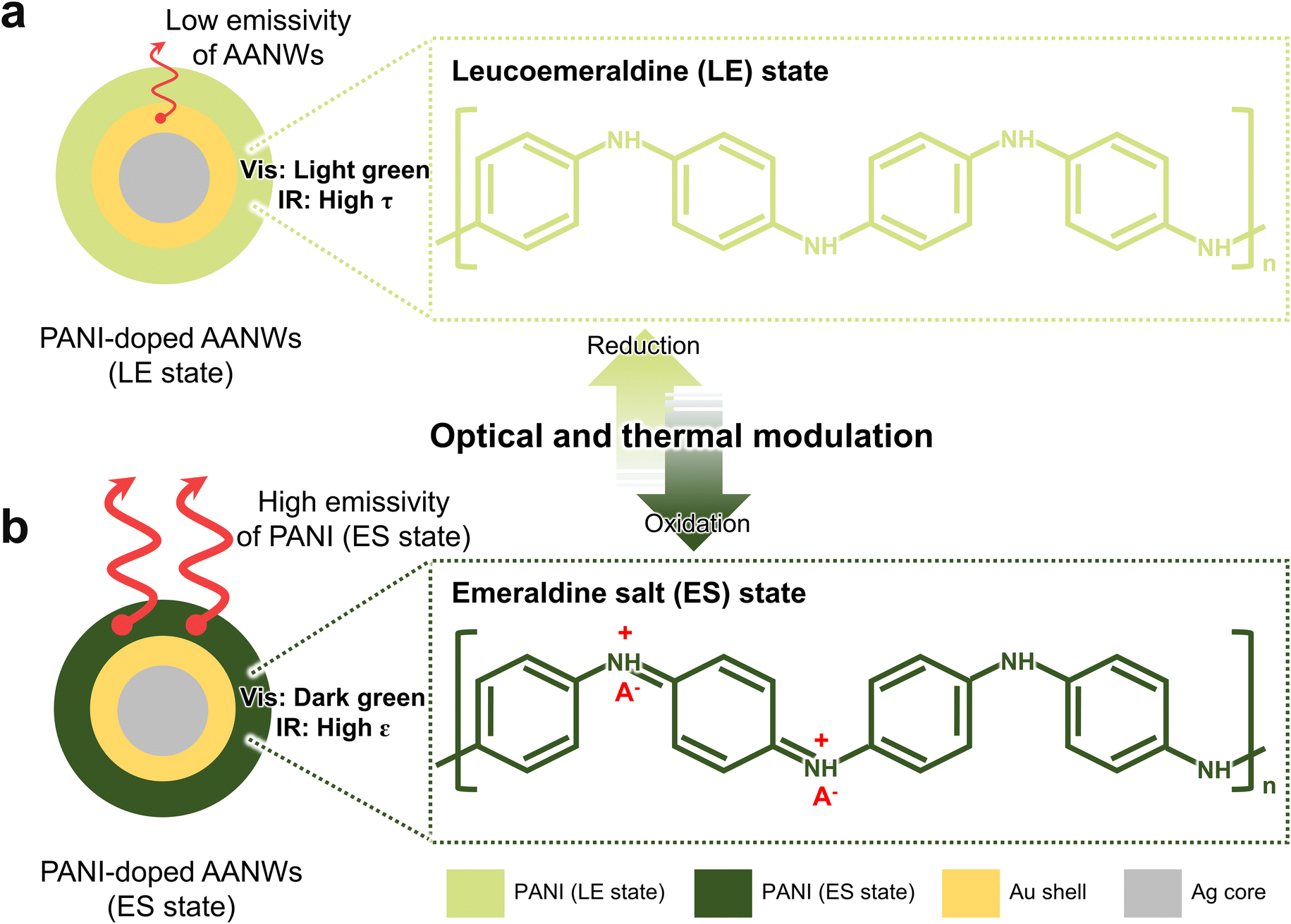 | ||
| Fig. 1 Mechanism of electrochromic effect for PANI-doped AANWs. (a) Optical and thermal properties of PANI-doped AANWs when PANI is in the LE state and (b) when PANI is in the ES state. | ||
However, the infrared optical modulation of PANI-doped AANWs, on the other hand, follows a different phenomenon. Fig. 1a and b explain the underlying mechanism for the emissivity change of PANI-doped AANWs in the infrared region. When in the LE state, PANI becomes highly transparent in the infrared region, as a result it displays low emissivity of Au and Ag, which are the inner layers of the multi-layered core–shell NWs (Fig. 1a). However, the ES state exhibits low transmittance and high emissivity as illustrated in Fig. 1b, so PANI in the ES state on the outer surface of the core–shell NWs serves to ‘mask’ the optical properties of Au and Ag with its high emissivity.12 In other words, the infrared emissivity change for PANI-doped AANWs directly corresponds to the emissivity difference of Au/Ag and PANI in the ES state.
The graphical representation in Fig. 2a illustrates a series of fabrication processes for PANI-doped AANWs in three essential steps. With the synthesized AANWs based on the modified method previously reported by our group,38 we utilized the vacuum filtration of AANWs on a hydrophilic porous polyethersulfone (PES) substrate to produce a thin film of the core–shell NWs. Fig. S1† shows the scanning electron microscopy (SEM) image of the porous PES substrate that we utilized in this work. Subsequently, selective laser irradiation on the NWs serves to weld their junctions by providing sufficient thermal energy to forge an electrically conductive NW network. Here, the laser annealing process not only enhances the electrical conductivity of the NW network but also strengthens the mechanical adhesion of the NWs and the substrate. Therefore, simple water rinsing only removes the NWs that have not been laser-welded, leaving the mechanically stable NW electrode behind. This process enables a direct patterning of the NW electrode into the desired shape at room temperature and in an ambient atmosphere without resorting to a rather expensive and complicated lithography technique. Finally, the following electrodeposition process conformally laminates PANI on top of the Au layer of AANWs.
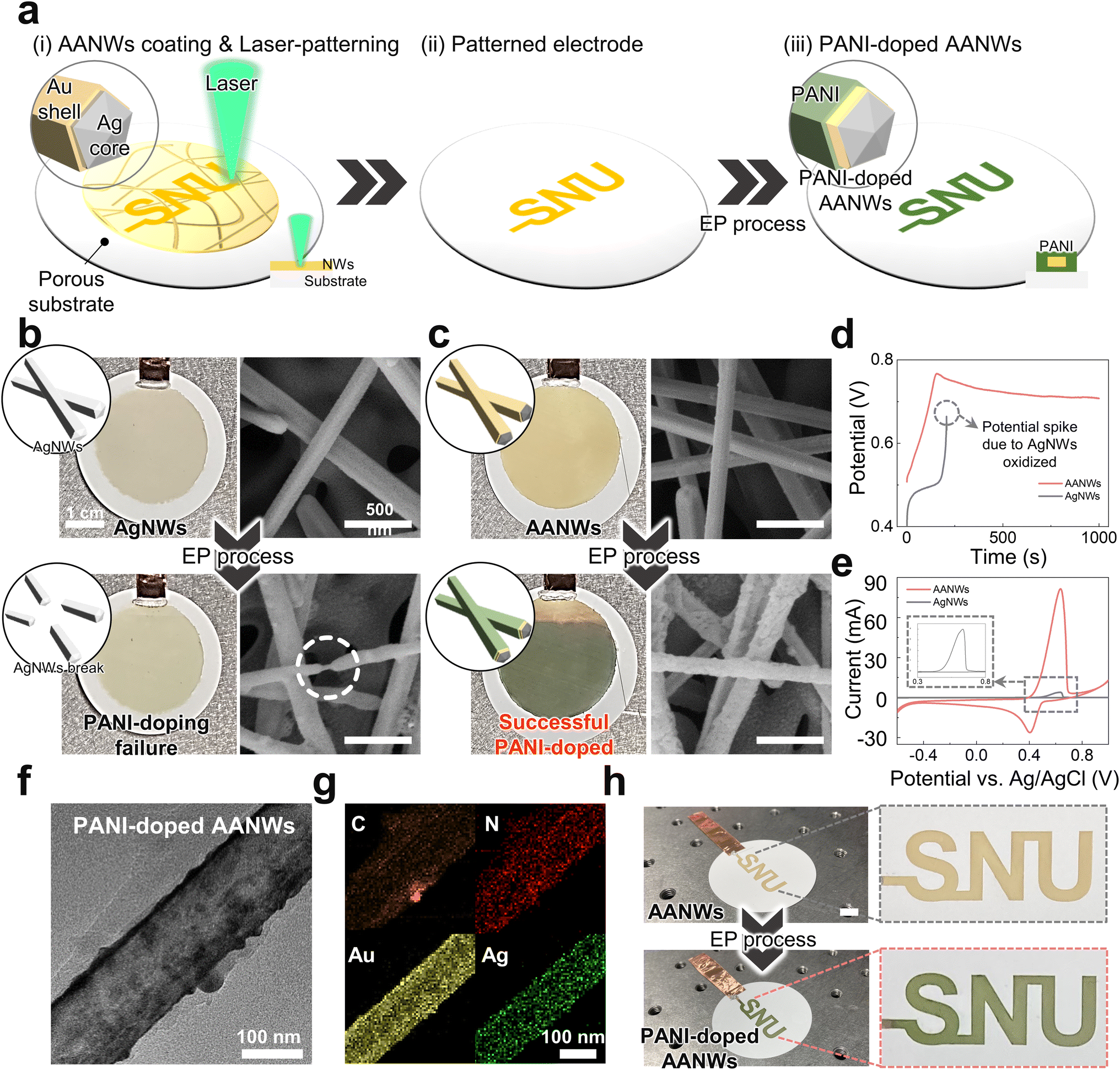 | ||
| Fig. 2 Fabrication process and material characterization of PANI-doped AANWs. (a) Simplified illustration of fabrication steps to make PANI-doped AANWs. (b) Visible light snapshot and SEM images of pristine AgNWs and AgNWs after PANI electrodeposition. When PANI is electrodeposited on AgNWs, the process causes the Ag oxidation and mechanical fracture of AgNWs. (c) Visible light snapshot and SEM images of pristine AANWs and AANWs after PANI electrodeposition. (d) Voltage profile of AgNWs and AANWs when PANI is being electrodeposited. (e) Cyclic voltammetry analysis of AANWs and AgNWs. The inset figure shows the magnified view of the cyclic voltammetry of AgNWs. (f) A TEM image of PANI-doped AANWs. (g) EDX of PANI-doped AANWs. (h) Snapshots of laser-patterned AANW and PANI-doped AANW electrodes. | ||
The Au layer in this work acts as an anti-oxidative agent as it prevents the oxidation of silver during the electrodeposition of PANI. The top view of the electrode and SEM image in Fig. 2b shows that the direct electrodeposition process of PANI does not occur on the surface of AgNWs. In fact, it causes the NWs to break into parts due to the instant oxidation of silver,39 whereas the electrodeposition on AANWs produces PANI-laminated core–shell NWs due to the electrochemical stability of Au. The SEM image in Fig. 2c implies that the NWs do not become fractured during the PANI electrodeposition. Furthermore, the increased thickness and relatively rough texture of NWs in the SEM image prove that PANI conformally laminates the AANWs . The voltage curve of constant current electrodeposition for PANI growth on the NW surface as in Fig. 2d substantiates this point. Compared to AANWs which depict a gradual increase and a successive plateauing of voltage over time, AgNWs produce an abrupt voltage spike as they are instantly oxidized. Likewise, the cyclic voltammetry (CV) analysis in Fig. 2e also offers electrochemical evidence of AgNW oxidation. The result shows that AgNWs only exhibit a tiny oxidation peak during the forward scan as in the inset of the figure whereas AANWs show much larger oxidation and reduction peaks. All of these results corroborate that the oxidation occurs shortly after electrodeposition of PANI starts, and the oxidation of silver in the course of electrodeposition creates an electrochemical barrier for the PANI nucleation on the surface of AgNWs. The transmission electron microscopy (TEM) images in Fig. 2f present the synthesized PANI-doped AANWs and show that the diameter of the multi-layered core–shell is approximately 170 nm. AgNWs, which we synthesized in this work, are 140 nm thick and 50–70 μm long, suggesting that the PANI–Au shell has a thickness of 30 nm. The chemical composition of carbon and nitrogen from the energy-dispersive X-ray spectroscopy (EDX) results in Fig. 2g implies the presence of the PANI lamination as a shell of the NW. Also, Raman spectroscopy offers the chemical bonding analysis for carbon-based and conductive polymers, and Fig. S2† compares the Raman intensity of PANI-doped AANWs and pristine AANWs. The result confirms the presence of PANI as an NW shell because the PANI-doped AANWs contain the intrinsic Raman peaks of PANI at 1178 cm−1 and 1600 cm−1, each of which is related to the C–C stretching vibration of benzene and C–H vibrations of aromatic rings of PANI, respectively.40,41 Lastly, the thermogravimetric analysis (TGA) results in Fig. S3† imply that the weight composition of PANI and AANWs respectively corresponds to 52% and 48% because AANWs does not experience a substantial weight reduction throughout the course of temperature elevation up to 800 °C. Meanwhile, the pristine AANWs do not contain any of these peaks since they are solely comprised of metals. Fig. 2h presents the laser-patterned electrode (the alphabet letters, S, N, U) based on AANWs and PANI-doped AANWs after electrodeposition of PANI on AANWs.
Fig. 3 characterizes the optical properties of the PANI-doped AANWs during their transformation from the ES state into the LE state. First, we optimized the electrodeposition condition of PANI to maximize its optical property modulation, so we used polymerization charge as a measure of the electrodeposition condition for PANI since the polymerization charge is directly correlated with the thickness of PANI (Fig. S4†). Fig. 3a reveals the considerable effect of polymerization charge on the emissivity change for both LE and ES states, suggesting the importance of material optimization. For instance, at the polymerization charge of 2C, there is only a negligible difference in the emissivity between the two redox states, and the emissivity difference begins to widen from 3C. The polymerization charge of 4C produces the maximum emissivity difference of 0.34, which then decreases starting from 5C. We also measured the infrared emissivity of PANI-doped AANWs that were electrodeposited with the polymerization charge of 4C using Fourier-transform infrared spectroscopy (FTIR) as in Fig. 3b. The electrical voltage input from −0.2 V to 0.7 V resulted in a dramatic emissivity increase in the infrared wavelength range, suggesting that the electrical input can be utilized to modulate the emissivity of the NW composite structure. In addition to the infrared emissivity modulation, the electrical input to the 4C sample affects the visible reflectance of the composite. For instance, as the electrical input voltage varies from −0.2 V to 0.7 V, the peak of visible reflectance shifts from 600 nm to 500 nm (Fig. 3c).
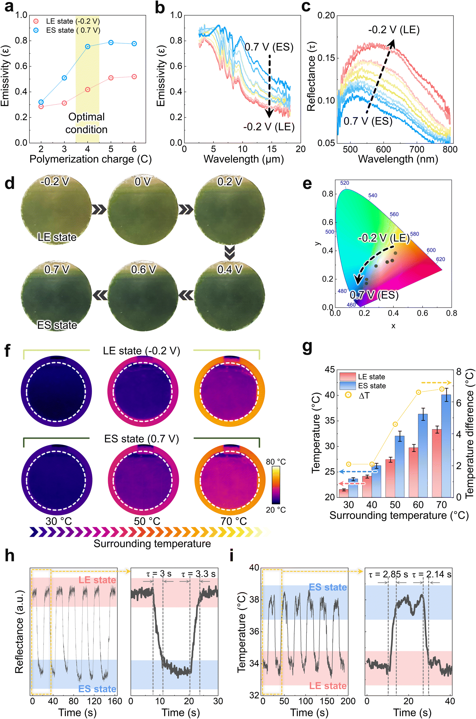 | ||
| Fig. 3 Optical characterization of PANI-doped AANWs. (a) Emissivity difference between the LE and ES states of PANI-doped AANWs with varying polymerization charge. (b) FTIR analysis of PANI-doped AANWs in the LE and ES states. (c) UV-Vis analysis of PANI-doped AANWs in the LE and ES states. (d) Visible light photographs of PANI-doped AANWs at different voltage inputs from −0.2 V to 0.7 V. (e) 1931 CIE diagram with the points of PANI-doped AANWs from −0.2 V to 0.7 V. (f) Infrared light photographs of PANI-doped AANWs at different voltage inputs from −0.2 V to 0.7 V. (g) Temperature and temperature difference between the LE and ES states in relation to the surrounding temperature. (h) The reflectance of PANI-doped AANWs as the material is repeatedly switched between two states. The inset figure shows the magnified view from 0 s to 30 s. (i) The temperature profile of PANI-doped AANWs as it is switched between two states. The inset figure shows the magnified view from 0 s to 40 s. | ||
To visualize the results in Fig. 3b andc, we captured the visible light and infrared thermal images of the PANI-doped AANW full-cell device in the course of the state transition as shown in Fig. 3d and f. For the full-cell device assembly, we sandwiched two films of PANI-doped AANWs with the gel-based electrolyte in between, and for the gel electrolyte, we used poly 2-acrylamido-2-methyl-1-propanesulphonic acid (PAMPS) and hydrochloric acid (HClO4), which can prevent electrolyte leakage and yet facilitate ion diffusion. When −0.2 V is applied to the sample, it produces the moccasin green color and is then converted into lunar green at 0.7 V. Fig. 3e exhibits the corresponding electrochromic shift from the light to the dark green chromatic coordinates within the 1931 CIE color gamut as PANI transforms from the LE state into the ES state. Besides the electrochromic properties of PANI-doped AANWs, the LE and ES states of the NW composite demonstrate a distinctive emissivity difference. Fig. 3f presents the infrared (IR) camera snapshots of each state at different surrounding temperatures, and it indicates that the ES state shows a much higher temperature than the LE state at the same surrounding temperature. The temperature discrepancy under the identical thermal condition presumably originates from the emissivity change in accordance with the surrounding temperature. To present it in a quantified manner, Fig. 3g shows the temperature of PANI at LE and ES states, and it indicates that ΔT starts to widen as the surrounding temperature increases. For instance, at 30 °C and 40 °C of the surrounding temperature, the temperature difference remained at around 2 °C, but it started to escalate rapidly up to about 7 °C when the surrounding temperature was raised up to 70 °C. Therefore, the overall result implies that the single input source can be used to modulate both the visible and IR emissivity difference of PANI-doped AANWs, thus validating its potential usage for data encryption display.
To test the cyclic switchability of PANI-doped AANWs between LE and ES states, we measured optical reflectance while alternating the states of PANI repeatedly as in Fig. 3h. PANI-doped AANWs demonstrated decent reliability to switch between the LE and ES states as it generated consistent optical output in a highly controlled manner. Also, the NW composite exhibits a rapid response time to convert from one state to the other interchangeably. The result shows that it takes less than 3.3 seconds to switch between the LE and ES states as it is depicted in the magnified view. Likewise, we measured the temperature of PANI-doped AANWs with the IR camera during repeated alternation between two states to verify its consistency to reproduce the temperature change by emissivity modulation (Fig. 3i). Just like the reflection change, the NW composite also exhibits a fast response time of less than 2.85 seconds to produce temperature change as it is converted to the LE state and back to the ES state. The rapid switchability between two redox states of the multilayered core–shell NWs shown herein serves as an essential feature for both electrochromic supercapacitor and encryption display applications because it would signify how much data the device can deliver to the user in a limited period of time.
To characterize PANI-doped AANWs for supercapacitor applications, we examined the capacitive performance by conducting CV tests with varying scanning rates of 5, 10, 20, 50, 100, and 200 mV s−1 with 1 M HClO4 gel-electrolyte (Fig. 4a). We set the voltage window as −0.2 V and 0.7 V to match the device operating range of the optical and thermal modulation. The CV curve illustrates a classical supercapacitive feature, and this geometrical characteristic is well preserved even when the CV is swept with high scanning rates, owing to the high surface area and chemical stability of PANI-doped AANWs. The galvanostatic charge–discharge (GCD) curves of Fig. 4b depict highly symmetrical triangles, which indicate the supercapacitive characteristic of the NW composite during the charging/discharging processes.42 From the GCD curves, the specific areal capacitance of the device was calculated to be 40.2, 37.1, and 34.1 mF cm−2 at 0.1, 0.5, and 1 mA cm−2 respectively, which is comparable to the previous NW-based supercapacitors without electrochromic properties (Table 1). Indeed, when compared with the recent supercapacitor studies, the specific areal capacitance of this work is lower than that of rigid devices and comparable to flexible devices. The reason for the slightly lower supercapacitive performance originates from the flexibility and electrochromic characteristics of the device as shown in Table S1.† It requires a large mass loading of PANI to attain high areal capacitance, but the excessive mass loading exerts a negative effect on flexibility and electrochromic properties. Especially, the excessive mass loading can negate the IR modulation capability of PANI-doped AANWs because it can affect the optical properties of the material composite. Also, the device in this study demonstrates a power density of 0.9 mW cm−2 and energy density of 4.525 μW cm−2 as presented in Fig. S5.†Fig. 4c shows the specific capacitance of the device with varying current density from 0.1 mA cm−2 to 2 mA cm−2, and it reveals that the current density of 2 mA cm−2 produces a specific capacitance of 30.11 mF cm−2, which corresponds to 75% of specific capacitance with 0.1 mA cm−2. Furthermore, we recorded the specific capacitance of the supercapacitor in relation to the cycle number as plotted in Fig. 4d, in which a single charging/discharging process corresponds to one cycle with 1 mA cm−2. The graph demonstrates that the device can retain a stable specific capacitance of over 80% of its original capacitance after 1000 GCD cycles. The reason for the degradation of capacitance retention mainly originates from the volume change of the PANI electrode as it shrinks and expands three-dimensionally during the charging and discharging processes. Such a volume change of the electrode causes a decrease in the electrical conductivity of the material and disturbs the chain structure of PANI over time.43
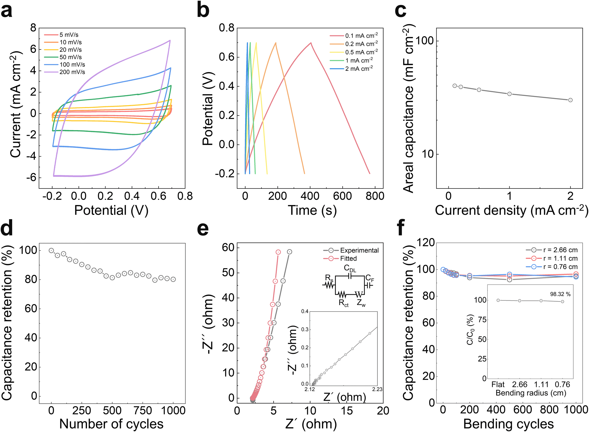 | ||
| Fig. 4 Characterization and performance evaluation of electrochromic supercapacitor application. (a) Cyclic voltammetry of the PANI-doped AANW-based supercapacitor with a scanning speed of 5 to 200 mV s−1. (b) Galvanostatic charging discharging profile of PANI-doped AANWs with different current densities of 0.1 to 2 mA cm−2. (c) Areal capacitance profile with varying current densities applied to the device. (d) Capacitance retention of the PANI-doped AANW supercapacitor in relation to the number of charging/discharging cycles. (e) Nyquist plot of the PANI-doped AANW supercapacitor, in which the graphs in gray and red correspond to experimental and equivalent circuit model data, respectively. The inset figure magnifies the high-frequency region of the Nyquist plot. (f) Capacitance retention of the PANI-doped AANW supercapacitor in relation to the number of bending cycles with different bending radius curvatures. The inset figure demonstrates the capacitance retention of the device with decreasing bending radius curvature. | ||
| Ref. | Material | Areal specific capacitance | Electrochromic function |
|---|---|---|---|
| This work | Ag–Au-PANI NWs | 40.2, 37.1, and 34.1 mF cm − 2 at 0.1, 0.5, and 1 mA cm − 2 | Yes, in the infrared-visible region |
| 52 | Te/Au/MnO2 core–shell | 79.8 mF cm−2 at 0.4 mA cm−2 | No |
| 53 | AgNWs | 2.09 mF cm−2 at a scan rate of 5 mV s−1 | No |
| 54 | SiNWs | 0.18 to 0.14 mF cm−2 at 0.1 to 2.3 mA cm−2 | No |
| 55 | Cu3(HHTP)2 nanowire array | 41.1 μF cm−2 at 0.5 A g−1 | No |
| 56 | PEDOT:PSS-glued MoO3 | 15.7 mF cm−2 at 0.02 mA cm−2 | Transparent |
| 57 | Ru/Si NWs | 18 mF cm−2 at 1 mA cm−2 | No |
| 58 | α-MnO2 nanowires | 250 mF cm−2 at 0.5 mA | No |
| 59 | MnOOH/nitrogen-doped graphene hybrid nanowires | 173.2 mF cm−2 at current densities of 1 mA cm−2 | No |
| 60 | MnO2 porous nanowires | Maximum value of 24.7 mF cm−2 at 0.1 mA cm−2 | No |
| 61 | Cu@CuO nanowires/carbon nanotubes | 193.8 mF cm−2 at 0.002 A cm−2 | No |
Moreover, the Nyquist plot in Fig. 4e allows us to examine the electrochemical properties of the PANI-doped AANW-based supercapacitor. The real-axis intercept in the high-frequency region of the Nyquist plot corresponds to the equivalent series resistance (ESR) or the cumulative resistance of the entire device system that includes the NW electrode, electrolyte, and interfacial contacts.44 The inset figure demonstrates an extremely low ESR value of 2.12 Ω, owing to the outstanding electrical conductivity of the plasmonically nano-welded NW network. In addition to the ESR, the absence of a semi-circle in the high-frequency region in the plot signifies a rapid charge transfer at the interface between the electrode and electrolyte, and the 45° Warburg element in the intermediate frequency region indicates the rapid ion diffusion at the interfacial surface.44–47 These electrochemical properties of PANI-doped AANWs generally arise from the high electrical conductivity and large surface area of the NW network, thus confirming the outstanding supercapacitor performance of the NW composite that was discussed earlier. We also compared the experimental result with the simulated result derived from the equivalent circuit in the inset of the figure. In the equivalent circuit diagram, Rs corresponds to the resistance that arises from the electrolyte ionic conductivity and electronic conductivity of the electrodes, where Rs value can be derived from the x-intercept at the high-frequency region. CDL represents double-layer capacitance, and Rct is the charge-transfer resistance that originates from the faradaic reactions. Finally, ZW is the Warburg impedance from the ion diffusion and CF signifies the resistance of ionic conductivity.48 The values we used for the equivalent circuit parameters such as Rs, CDL, Rct, Zw and CF are 2.218 Ω, 12.08 F, 237.5 Ω, 1.01 × 10⁻⁵ S s−0.5, and 0.246 F, respectively. The simulated result from the equivalent circuit highly resembles the experimental data, considering that they both have very close Rs values and do not display a semi-circle in the high-frequency region. The only major difference between the two plots is the slope in the low-frequency region: the simulated result shows a steeper slope, signifying an ideal capacitor behavior. Utilizing NWs as a backbone material offers mechanical stability to withstand a high degree of mechanical stress, so we tested the mechanical robustness of PANI-doped AANWs as shown in Fig. 4f, where we applied cyclic bending stress to the device because one of the main causes of mechanical failure for mechanically deformable electronics originates from fatigue stress. The bending test result suggests that the device is capable of retaining normalized capacitance that is higher than 94.5% of its original capacitance even after 1000 bending cycles for all bending radius curvatures of 0.76, 1.11, and 2.66 cm as demonstrated in Fig. S6.† Besides the fatigue stress, the inset of Fig. 4f indicates that the supercapacitor can retain 98.3% of its capacitance when a bending radius curvature of 0.76 cm is applied. The result illustrates that the supercapacitor presented herein can maintain a stable charging/discharging characteristic regardless of external mechanical force. Based on these figures, we expect that the device's capability to resist a high magnitude of external mechanical stress allows its potential applications to be utilized on the highly deformable surface or further employed for wearable purposes.
Another practical application of PANI-doped AANWs lies in the display technology since the PANI-doped AANWs based full-cell with the gel-electrolyte resembles the electrochromic display architecture. Fig. 5a presents the graphical illustration of the data encryptable display architecture, in which two layers of PANI-doped AANWs on the hydrophilic PES porous membranes sandwich the gel electrolyte with the nanowire composites facing outward. Then, selective laser ablation electrically disconnects the electrode to be displayed from the background electrode. For example, we laser-ablated the perimeter of the alphabet letters, S, N, and U, such that these letters can stand out by the electrochromic effect when 0.7 V is applied to induce the ES state. Thus, since the rest of the electrode remains in the LE state, the patterned electrode can be encrypted if it is in the LE state, and it can readily be decrypted if it turns into the ES state. Fig. 5b shows the full-cell device, and it can operate as a data encryption display for both the visible and infrared wavelength realms. Fig. 5c demonstrates the snapshots of device encryption and decryption that were captured with the visible camera and infrared thermal imaging cameras. The encrypted letters can be clearly observed when 0.7 V is applied to oxidize the patterned region for both the visible and infrared wavelengths.
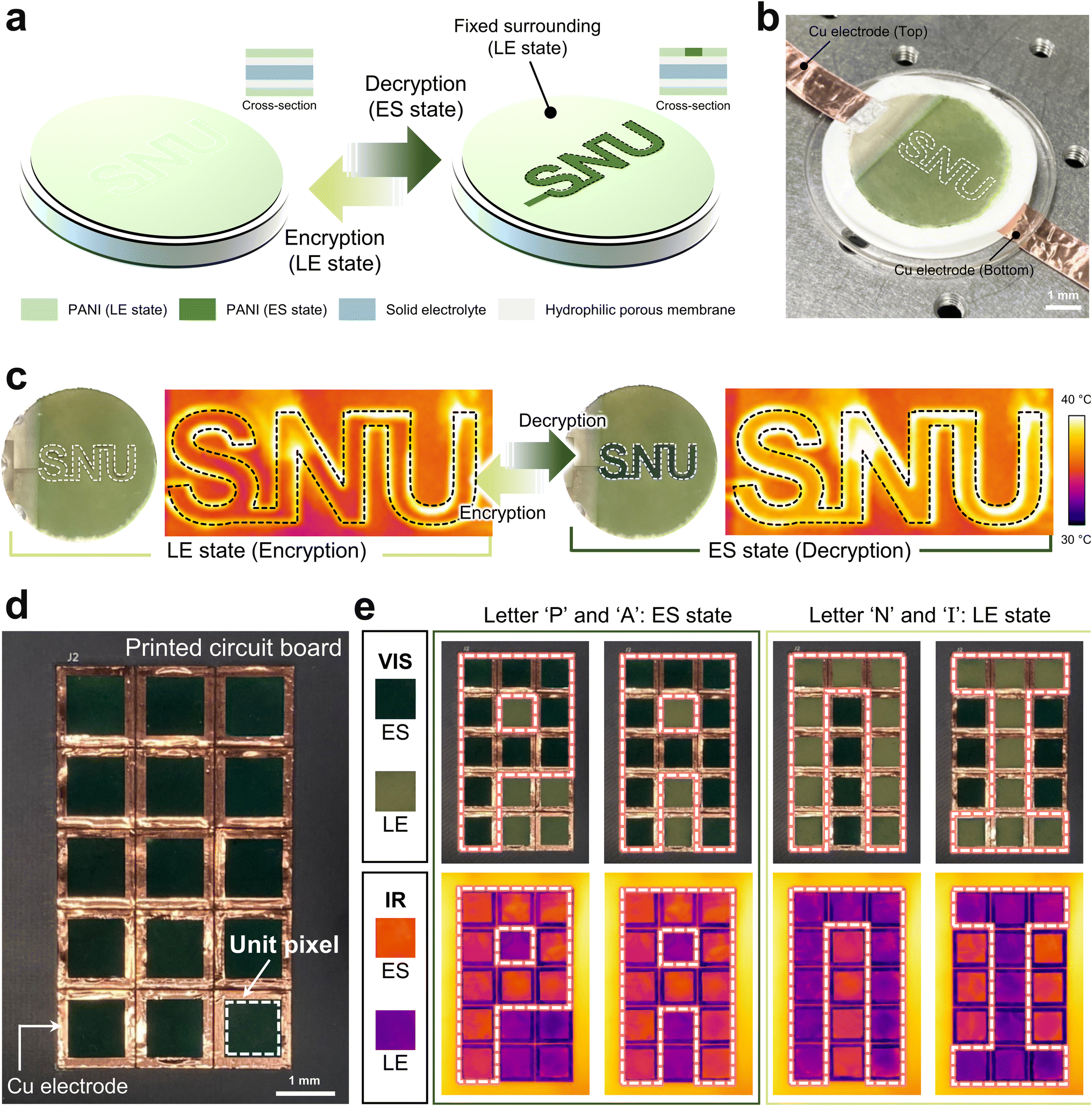 | ||
| Fig. 5 Data encryptable display application. (a) Graphical illustration of the full cell device for the display application. (b) Top view photograph of the full-cell device. (c) Laser patterned display device in swtiching between the encryption and decryption mode that displays the alphabets, SNU, in the visible light and IR views. (d) Top view of the multi-pixel display device with PCB integration. (e) Multi-pixel display device that displays the word, PANI, in visible light and IR views. | ||
Besides the laser patterned region, another type of display system can be made by assembling multiple miniature electrochromic devices such that each device unit works as a pixel. Fig. 5d demonstrates the multi-pixel display consisting of a 3 × 5 pixel array, and the printed circuit board provides the programmed electrical input to each pixel such that, for instance, it can display the desired alphabet letter. Fig. 5e shows that the letters, P, A, N, and I, are decrypted as certain pixels are converted to the ES state, while the rest of the pixels stay in the LE state. To corroborate that the multi-pixel display operates properly as programmed, we applied two different inputs to show the alphabet letters in the figure: the letters, P and A, are converted to the ES state whereas the pixels other than the letters, N and I, switched into the ES states. As for the multi-pixel display, the visible and infrared snapshots, which were taken by the visible light and infrared thermal imaging cameras respectively, substantiate that the multi-pixel display operates well with high visibility for both the visible and infrared wavelengths.
Conclusion
In this work, we demonstrated a polymer–metal multilayered NW network that can function both as a multispectral electrochromic supercapacitor and data encryptable display. The laser irradiation allowed the selective sintering of the NWs and patterning of the electrode, and the subsequent electrodeposition of PANI fully functionalized the NWs into practical smart devices. The electrochromic supercapacitor based on PANI-doped AANWs showed a high specific capacitance of 40.2 mF cm−2 at 0.1 mA cm−2 and is capable of displaying the level of energy stored by its varying optical properties. Besides the supercapacitor device, we also developed two types of data encryptable display platforms: patterned and multi-pixel displays. These display platforms deliver visual information when a certain part of the electrode region is converted into the ES state and changes the optical properties while the rest of the electrode remains in the LE state. Owing to the material design and deliberate optimization of PANI-doped AANWs, the electrochromic device based on PANI can modulate its optical properties both in visible and infrared wavelength spectra for the first time. In this regard, we expect that all the results and smart devices presented in this work will contribute to the development of next-generation nanomaterials and innovative device technologies.Experimental section
Synthesis of Ag–Au core–shell nanowires
The Ag–Au core–shell nanowires were synthesized by harnessing similar methods that have been reported.38,49,50 In order to prepare the Au growth solution, 30 mg of hydrogen tetrachloroaurate(III) hydrate (HAuCl4·xH2O, FW 339.79, Sigma-Aldrich) and 17 mg of sodium hydroxide (NaOH, Samchun Chemicals) were mixed in 70 ml of distilled water. After the color of the mixture turned from yellow to transparent, 33 mg of sodium sulfite (Na2SO3, Sigma-Aldrich) was added. Another solution was prepared by dissolving 800 mg of poly(vinylpyrrolidone) (PVP, Mw 55,000, Sigma-Aldrich), 70 mg of NaOH, 300 mg of L-ascorbic acid (L-AA, Samchun Chemicals), and 10 mg of Na2SO3 into 100 ml of Ag nanowire solution (Ag: 20 mg). Consequently, the Au growth solution was gently mixed with the solution containing Ag nanowires. After 30 minutes, the Au shell was well attached to the core Ag nanowires. Finally, the synthesized core–shell nanowires were washed several times through centrifugation and utilized by dispersing them into isopropanol.Preparation of the AANW electrode
The synthesized AANWs were deposited onto a PES membrane (Sigma-Aldrich) via vacuum filtration. Subsequently, the deposited AANWs were laser-annealed using a 532 nm continuous wave laser (Sprout-G-5W, Lighthouse Photonics) at a power of 0.3 mW, and a scanning speed of 350 mm s−1.Preparation of PANI-doped AANW films
The electropolymerization of PANI films was conducted using an electrochemical workstation (VersaSTAT 3, Princeton Applied Research) with a three-electrode system, consisting of an AANW electrode as the working electrode, a platinum (Pt) mesh electrode as the counter electrode, and an Ag/AgCl electrode as the reference electrode. The as-fabricated AANW electrode was submerged into a solution of 1 M hydrochloric acid (HClO4, SAMCHUN Chemicals) and 0.5 M aniline (SAMCHUN Chemicals), and then electropolymerization was carried out at a constant current density of 0.2 mA cm−2. Subsequently, the resulting electropolymerized PANI films were rinsed with deionized water.Material characterization
The scanning electron microscopy (SEM) images and transmission electron microscopy (TEM) images were acquired using a JSM-7600f from JEOL and Tecnai F20 from FEI, respectively. In addition, Raman spectra were obtained using a Raman micro-spectroscopy system (Renishaw inVia-reflex model with a 514 nm diode laser).Optical measurement
The visible reflectance spectra and infrared emissivity spectra of the PANI-doped AANW films were measured using a UV-Vis (V-770, Jasco) spectroscopy system and an FTIR (Spectrum Paragon, PerkinElmer) spectroscopy system, respectively. The temperature graph of the thermal images was measured with an IR camera (FLIR A645 sc).Assembly of the full-cell device
The gel electrolyte was prepared as described previously in ref. 51. In brief, the monomer (2-acrylamido-2-methyl-1-propanesulfonic acid) and cross-linker (N,N′-methylenebis (acrylamide)) were dissolved in 1 M HClO4 solution. After the solution became transparent, the initiator (ammonium persulfate) was added to the solution. Subsequently, the solution was poured into a mold and treated at 60 °C for 3 hours to form the gel electrolyte. Two identical sets of PANI-doped AANW films were prepared and their ends were connected to a copper electrode. Finally, the full-cell device was assembled by converting two PANI-doped AANW films on both sides of the gel electrolyte.Electrochemical performance measurement of the supercapacitor
The electrochemical properties of supercapacitors were measured using an electrochemical workstation (VersaSTAT 3, Princeton Applied Research) with a two-electrode test method.Preparation of the encryptable device
As-fabricated PANI-doped AANW films were patterned into the desired design (the word ‘SNU’) via a laser ablation process using a 355 nm pulsed laser (Nanio Air 355-3-V, InnoLas Photonics) with a two-axis galvano micro-scanner.Preparation of a 3 × 5 pixel array
As-prepared PANI-doped AANW films were cut into the desired size (1 mm × 1 mm). The square-shaped PANI-doped AANW unit film was integrated into the printed circuit board to form a 3 × 5 pixel array.Author contributions
Y. J. and K. R. P. contributed equally to this work. Y. J. and K. R. P. conceived the work. J. M. and H. Y. synthesized the AgNWs and Ag–Au core–shell wires. Y. J. and K. R. P. prepared all the samples for the optical characterization of PANI-doped AANWs. Y. J., K. R. P. and J. L. conducted the experiments for supercapacitor characterization, and Y. J. and K. R. P. designed and obtained the data for the encryptable display device. Y. J., K. R. P., M. L., B. K., J. L., and S. H. K. discussed the outcomes. J. L. wrote the manuscript and S. H. K. revised the manuscript. S. H. K. funded and directed the overall project.Conflicts of interest
The authors declare no conflict of interest.Acknowledgements
This work was supported by the National Research Foundation of Korea (NRF) Grant (NRF-2021R1A2B5B03001691) and the Hyundai Motor Company (HR-210433.0003).References
- F. Kazemi, S. Naghib and Z. Mohammadpour, Mater. Today Chem., 2020, 16, 100249 CrossRef CAS.
- R. Tanwar, B. Kaur and U. K. Mandal, Appl. Catal., B, 2017, 211, 305–322 CrossRef CAS.
- L. Kumar, I. Rawal, A. Kaur and S. Annapoorni, Sens. Actuators, B, 2017, 240, 408–416 CrossRef CAS.
- G. Shim, M. X. Tran, G. Liu, D. Byun and J. K. Lee, Energy Storage Mater., 2021, 35, 739–749 CrossRef.
- P. Luo, Y. Xiao, J. Yang, C. Zuo, F. Xiong, C. Tang, G. Liu, W. Zhang, W. Tang and S. Wang, Chem. Eng. J., 2022, 433, 133772 CrossRef CAS.
- L. Wang, X. Feng, L. Ren, Q. Piao, J. Zhong, Y. Wang, H. Li, Y. Chen and B. Wang, J. Am. Chem. Soc., 2015, 137, 4920–4923 CrossRef CAS PubMed.
- X. Wang, D. Zhang, H. Zhang, L. Gong, Y. Yang, W. Zhao, S. Yu, Y. Yin and D. Sun, Nano Energy, 2021, 88, 106242 CrossRef CAS.
- X. Huang, Q. Niu, S. Fan and Y. Zhang, Chem. Eng. J., 2021, 417, 128126 CrossRef CAS.
- T. An, Y. Ling, S. Gong, B. Zhu, Y. Zhao, D. Dong, L. W. Yap, Y. Wang and W. Cheng, Adv. Mater. Technol., 2019, 4, 1800473 CrossRef.
- P. Yang, P. Sun and W. Mai, Mater. Today, 2016, 19, 394–402 CrossRef CAS.
- K. Zhou, H. Wang, J. Jiu, J. Liu, H. Yan and K. Suganuma, Chem. Eng. J., 2018, 345, 290–299 CrossRef CAS.
- L. Zhang, B. Wang, X. Li, G. Xu, S. Dou, X. Zhang, X. Chen, J. Zhao, K. Zhang and Y. Li, J. Mater. Chem. C, 2019, 7, 9878–9891 RSC.
- H. Li, K. Xie, Y. Pan, M. Yao and C. Xin, Synth. Met., 2009, 159, 1386–1388 CrossRef CAS.
- J. Jung, H. Cho, R. Yuksel, D. Kim, H. Lee, J. Kwon, P. Lee, J. Yeo, S. Hong and H. E. Unalan, Nanoscale, 2019, 11, 20356–20378 RSC.
- J. Jung, H. Lee, I. Ha, H. Cho, K. K. Kim, J. Kwon, P. Won, S. Hong and S. H. Ko, ACS Appl. Mater. Interfaces, 2017, 9, 44609–44616 CrossRef CAS PubMed.
- K. Liu, W. Liu, W. Li, Y. Duan, K. Zhou, S. Zhang, S. Ni, T. Xu, H. Du and C. Si, Adv. Compos. Hybrid Mater., 2022, 5, 1078–1089 CrossRef CAS.
- P. Won, J. J. Park, T. Lee, I. Ha, S. Han, M. Choi, J. Lee, S. Hong, K.-J. Cho and S. H. Ko, Nano Lett., 2019, 19, 6087–6096 CrossRef CAS PubMed.
- D. Kim, J. Bang, W. Lee, I. Ha, J. Lee, H. Eom, M. Kim, J. Park, J. Choi and J. Kwon, J. Mater. Chem. A, 2020, 8, 8281–8291 RSC.
- M. Razeghi, M. Üstünçelik, F. Shabani, H. V. Demir and T. S. Kasırga, Nanoscale Horiz., 2022, 7, 396–402 RSC.
- B. Shi, T. Wang, L. Shi, J. Li, R. Wang and J. Sun, Appl. Mater. Today, 2020, 19, 100610 CrossRef.
- S. Han, J. Kim, Y. Lee, J. Bang, C. G. Kim, J. Choi, J. Min, I. Ha, Y. Yoon and C.-H. Yun, Nano Lett., 2021, 22, 524–532 CrossRef PubMed.
- W. Seo, D. Kim, S. Kim and H. Lee, Materials, 2021, 14, 3934 CrossRef CAS PubMed.
- S. Wang, H. Xu, T. Hao, M. Xu, J. Xue, J. Zhao and Y. Li, Appl. Surf. Sci., 2022, 577, 151889 CrossRef CAS.
- H. Moon, H. Lee, J. Kwon, Y. D. Suh, D. K. Kim, I. Ha, J. Yeo, S. Hong and S. H. Ko, Sci. Rep., 2017, 7, 1–10 CrossRef PubMed.
- R. Yuksel, E. Alpugan and H. E. Unalan, Org. Electron., 2018, 52, 272–280 CrossRef CAS.
- T. G. Yun, D. Kim, Y. H. Kim, M. Park, S. Hyun and S. M. Han, Adv. Mater., 2017, 29, 1606728 CrossRef PubMed.
- T. Hao, S. Wang, H. Xu, X. Zhang, J. Xue, S. Liu, Y. Song, Y. Li and J. Zhao, Chem. Eng. J., 2021, 426, 130840 CrossRef CAS.
- T. G. Yun, M. Park, D.-H. Kim, D. Kim, J. Y. Cheong, J. G. Bae, S. M. Han and I.-D. Kim, ACS Nano, 2019, 13, 3141–3150 CrossRef CAS PubMed.
- J. Lee, P. Lee, H. Lee, D. Lee, S. S. Lee and S. H. Ko, Nanoscale, 2012, 4, 6408–6414 RSC.
- S. Han, S. Hong, J. Ham, J. Yeo, J. Lee, B. Kang, P. Lee, J. Kwon, S. S. Lee and M. Y. Yang, Adv. Mater., 2014, 26, 5808–5814 CrossRef CAS PubMed.
- R.-R. Wang, M.-L. Zheng, W.-C. Zhang, J. Liu, T. Li, X.-Z. Dong and F. Jin, Nano Lett., 2022, 22, 9823–9830 CrossRef CAS PubMed.
- T. Ji, R. Tu, L. Mu, X. Lu and J. Zhu, Appl. Catal., B, 2018, 220, 581–588 CrossRef CAS.
- K. Zhu, Y. Gao, X. Tan and C. Chen, ACS Sustainable Chem. Eng., 2016, 4, 4361–4369 CrossRef CAS.
- D. Park, M. Kim and J. Kim, J. Alloys Compd., 2021, 884, 161098 CrossRef CAS.
- Z. Zhang, M. Liu, M. M. Ibrahim, H. Wu, Y. Wu, Y. Li, G. A. Mersal, I. H. El Azab, S. M. El-Bahy and M. Huang, Adv. Compos. Hybrid Mater., 2022, 5, 1054–1066 CrossRef CAS.
- H. Cheng, Y. Pan, Q. Chen, R. Che, G. Zheng, C. Liu, C. Shen and X. Liu, Adv. Compos. Hybrid Mater., 2021, 4, 505–513 CrossRef CAS.
- A. Korent, K. Ž. Soderžnik, S. Šturm and K. Ž. Rožman, J. Electrochem. Soc., 2020, 167, 106504 CrossRef CAS.
- H. Lee, S. Hong, J. Lee, Y. D. Suh, J. Kwon, H. Moon, H. Kim, J. Yeo and S. H. Ko, ACS Appl. Mater. Interfaces, 2016, 8, 15449–15458 CrossRef CAS PubMed.
- F.-W. Li, T.-C. Yen, S. Manavalan and G.-S. Liou, ACS Appl. Polym. Mater., 2021, 3, 2971–2978 CrossRef CAS.
- T. Fan, S. Tong, W. Zeng, Q. Niu, Y. Liu, C.-Y. Kao, J. Liu, W. Huang, Y. Min and A. J. Epstein, Synth. Met., 2015, 199, 79–86 CrossRef CAS.
- A. B. Rohom, P. U. Londhe, S. Mahapatra, S. Kulkarni and N. Chaure, High Perform. Polym., 2014, 26, 641–646 CrossRef.
- Y. Gogotsi and R. M. Penner, ACS Nano, 2018, 12, 2081–2083 CrossRef CAS PubMed.
- H. Wang, J. Lin and Z. X. Shen, J. Sci.: Adv. Mater. Devices, 2016, 1, 225–255 Search PubMed.
- J. Lee, J. Lee, J. Kwon, H. Lee, H. Eom, Y. Yoon, I. Ha, M. Yang and S. H. Ko, Langmuir, 2017, 33, 1854–1860 CrossRef CAS PubMed.
- S. Park, A. W. M. Tan, J. Wang and P. S. Lee, Nanoscale Horiz., 2017, 2, 199–204 RSC.
- X. Wang, C. Yan, A. Sumboja and P. S. Lee, Nano Energy, 2014, 3, 119–126 CrossRef CAS.
- J. Gamby, P. Taberna, P. Simon, J. Fauvarque and M. Chesneau, J. Power Sources, 2001, 101, 109–116 CrossRef CAS.
- M. Jiang and X. Zhang, J. Alloys Compd., 2019, 794, 13–20 CrossRef CAS.
- S. Choi, S. I. Han, D. Jung, H. J. Hwang, C. Lim, S. Bae, O. K. Park, C. M. Tschabrunn, M. Lee and S. Y. Bae, Nat. Nanotechnol., 2018, 13, 1048–1056 CrossRef CAS PubMed.
- M. Yang, Z. D. Hood, X. Yang, M. Chi and Y. Xia, Chem. Commun., 2017, 53, 1965–1968 RSC.
- Y. Jung, I. Ha, M. Kim, J. Ahn, J. Lee and S. H. Ko, Nano Energy, 2023, 105, 107979 CrossRef CAS.
- J. Cao, M. Safdar, Z. Wang and J. He, J. Mater. Chem. A, 2013, 1, 10024–10029 RSC.
- B. Wang, X. Zhao, J. Liang, J. Liu, Y. Yang, M. Zhang, H. Yu, J. Li, Y. Tong and Q. Tang, ACS Appl. Energy Mater., 2022, 5, 10490–10500 CrossRef CAS.
- T. Lé, P. Gentile, G. Bidan and D. Aradilla, Electrochim. Acta, 2017, 254, 368–374 CrossRef.
- X. Du, J. Zhang, H. Wang, Z. Huang, A. Guo, L. Zhao, Y. Niu, X. Li, B. Wu and Y. Liu, Mater. Chem. Front., 2020, 4, 243–251 RSC.
- J. Liang, H. Sheng, Q. Wang, J. Yuan, X. Zhang, Q. Su, E. Xie, W. Lan and C. J. Zhang, Nanoscale Adv., 2021, 3, 3502–3512 RSC.
- Y. Bencheikh, M. Harnois, R. Jijie, A. Addad, P. Roussel, S. Szunerits, T. Hadjersi, S. E. H. Abaidia and R. Boukherroub, Electrochim. Acta, 2019, 311, 150–159 CrossRef CAS.
- N. Bose, V. Sundararajan, T. Prasankumar and S. P. Jose, Mater. Lett., 2020, 278, 128457 CrossRef CAS.
- S. Yang, X. Song, P. Zhang and L. Gao, J. Mater. Chem. A, 2015, 3, 6136–6145 RSC.
- J. Song, H. Li, S. Li, H. Zhu, Y. Ge, S. Wang, X. Feng and Y. Liu, New J. Chem., 2017, 41, 3750–3757 RSC.
- H.-X. Zhao, Y.-L. Liu, G.-G. Wang, F. Li, G.-Z. Li, H.-L. Zhou, H.-Y. Zhang and J.-C. Han, Energy Technol., 2021, 9, 2000744 CrossRef CAS.
Footnotes |
| † Electronic supplementary information (ESI) available. See DOI: https://doi.org/10.1039/d3ta00426k |
| ‡ Y. Jung and K. R. Pyun equally contributed to this work. |
| This journal is © The Royal Society of Chemistry 2023 |