
 Open Access Article
 This Open Access Article is licensed under a
 Creative Commons Attribution 3.0 Unported Licence
The role of selective contacts and built-in field for charge separation and transport in photoelectrochemical devices
Markus
Schleuning
 *ab,
Ibbi Y.
Ahmet
a,
Roel
van de Krol
ab and
Matthias M.
May
cd
*ab,
Ibbi Y.
Ahmet
a,
Roel
van de Krol
ab and
Matthias M.
May
cd
aInstitute for Solar Fuels, Helmholtz-Zentrum Berlin für Materialien und Energie GmbH, Germany. E-mail: markus.schleuning@helmholtz-berlin.de
bInstitute of Chemistry, Technische Universität Berlin, Germany
cInstitute of Physical and Theoretical Chemistry, Universität Tübingen, Germany
dInstitute of Theoretical Chemistry, Universität Ulm, Germany
First published on 14th June 2022
Abstract
Direct photoelectrochemical (PEC) solar water splitting has the potential to be a key element in a sustainable energy supply chain. However, integrated PEC systems based on metal oxides still lack the high efficiencies required for large-scale, economically feasible applications. A main obstacle for the realization of higher solar-to-hydrogen efficiencies is the appropriate design of the semiconductor–catalyst and semiconductor–electrolyte interfaces. Thus, a more accurate understanding of the energy loss mechanisms and the driving forces that determine the charge separation, transport and recombination of electrons and holes in a PEC device would be instrumental for the selection of the most appropriate design routes. In this context we highlight a common misconception within the PEC research community, which is to consider the built-in electrical field at the solid/liquid interface as essential for charge separation. We subsequently emphasize the established viewpoint within the photovoltaic research community that the gradient of the electrochemical potential is the principle driving force for charge separation and efficient solar energy conversion. Based on this realization, we argue that improved contact design in PEC devices should be one of the main research directions in the design of PEC devices. To address this challenge, we take a closer look at how optimized contacts have been constructed so far and present potential design approaches which can be used to further improve the performance of PEC devices.
I Introduction
The use of solar energy is widely accepted as a key element of a sustainable energy system. However, large-scale storage must be feasible, as the local availability of sunlight on earth follows diurnal and seasonal cycles. Sustainably produced fuels are a very attractive way to store extensive amounts of energy for long periods of time. The established low-cost competitor for artificial solar energy harvesting is natural photosynthesis, yet efficiencies are at around 1%,1 which creates a land use conflict with food production. A simple and maybe the ‘cleanest’ chemical fuel is green H2, since only water vapor and no CO2 is released during its use.2–4 One way of producing green H2 is the approach of direct solar water splitting,5,6 where the light absorbing semiconductor is in direct contact with an aqueous electrolyte. It follows from the spectral distribution of the sunlight that tandem devices are needed to generate more than the minimum required photovoltage of 1.23 V plus overpotentials at current densities that allow efficient operation. Solar-to-hydrogen (STH) efficiencies close to 20% have been achieved already,7 using III–V semiconductors with functionalized surfaces.8–10 So far, quite large device costs, together with limited stability and difficulties in scale up, are among the obstacles towards mass production of PEC devices. This is why metal oxides (MOs) are considered a promising material class, as they offer more opportunities to utilize inexpensive, earth abundant and non toxic elements. However, the STH eff. of full MO tandem cells still exhibit low efficiencies around 1–3% and insufficient stabilities, which needs to be at least greater than 5 to 10 years.6,11,12 As a result, new oxide materials are being explored, but despite the intensive efforts by the community, breakthroughs towards commercially viable, highly efficient oxide-based devices have yet to be realized. This might also be a consequence of the underestimation of the importance of appropriate selective contacts, which has significant implications for the overall device design. It is important to realize that PEC devices work, on the opto-electronic level and regarding their thermodynamics, in full analogy to conventional photovoltaic (PV) cells. For PV devices, it is now well understood that the selectivity of the front and back contacts is a key feature needed for efficient charge separation and to finally deliver high current and voltage. Furthermore, the role of the built-in electric field (E-field) at the pn-junction had to be reevaluated, since it was shown to be incorrect to attribute the charge transport and separation just to the E-field at the junction.13–16 These important realizations have not yet been fully embraced by the PEC community.17 In the following, we provide arguments for a change in perspective regarding the way the charge separation takes place in PEC devices and we elaborate consequences for the construction of functional devices and their contacts. Since it is theoretically possible to separately consider and optimize the solar absorber and the electrochemical (EC) components of a PEC device,18,19 we will first focus on the absorber component. We begin with a brief review and reminder of the fundamental processes and forces that lead to the generation, transport, and separation of charge carriers in semiconductors. This is followed by a description of different concepts of “selective” contacts with a focus on solid/metal and solid/liquid interfaces. Finally, a comprehensive picture of a PEC cell under working conditions is given and possible routes towards higher efficiencies are presented. We conclude that the contact optimization is, just like the optimization of the bulk absorber properties, essential for efficient PEC devices.II Charge-separation and transport
A Questioning the role that the built-in electric field plays for charge separation
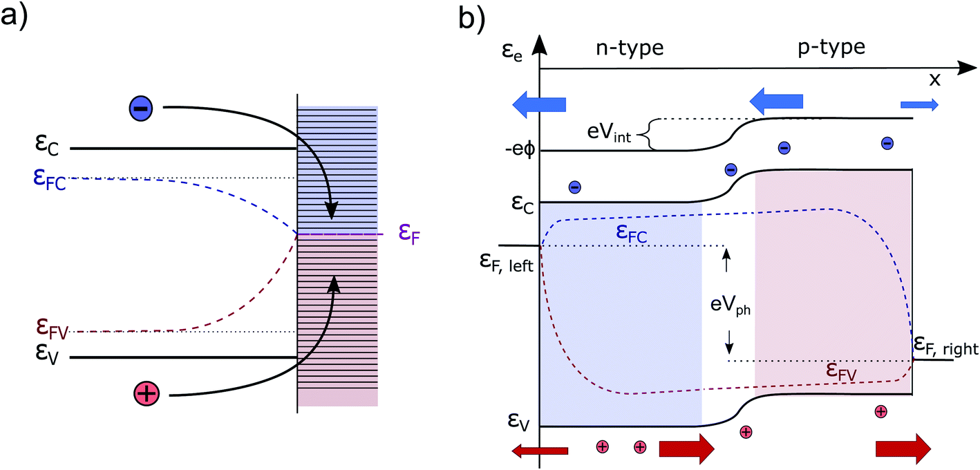
Currently, the most common interpretation of photocurrent generation from a photoelectrode within an electrolyte is to assume that the separation of electron–hole pairs takes place only in a region near the surface due to the presence of an internal electric field, originating from the band-bending at the solid/liquid interface established in dark equilibrium.17,20 This view is originally based on a description by Gärtner for the pn-junction.21 This internal electric field is often assumed to be an independent force which drives the charges (positive and negative) in opposite directions towards the respective contacts. However, there are several problematic aspects of this explanation. For instance there are well-known devices such as crystalline silicon (c-Si) solar cells, that are in fact by volume 99% free of any built-in field,15,22 but still represent the working horse of the world-wide PV market. Also dye-synthesized solar cells (DSSCs) are known to be practically field-free due to the screening by the electrolyte solution.23 This is also true for nanostructured PEC devices, which cannot be expected to develop a significant space charge layer due to their spatial limitations.24 Even more important are the theoretical inconsistencies of this explanation as outlined by Würfel.14 First, if an electric field accelerates charges its potential energy is converted into kinetic energy. Inside of a (semi-)conductor, this kinetic energy is partially dissipated during scattering events, resulting in unavoidable ohmic losses. Continuous charge separation requires a constant acceleration of charges and, therefore, a constant energy input in order not to violate the first law of thermodynamics. This energy can only be provided by an external source, such as an external applied voltage or by incident sunlight. Consider now a semiconductor junction in equilibrium, i.e., in the dark and without any applied potential. Even though an electric field is typically present in such a junction (the so-called ‘built-in’ field), no net charge separation occurs. However, charge separation does occur when the junction is illuminated, even though continuous illumination, followed by charge redistribution, actually reduces the magnitude of the electric field at the junction.25 This clearly implies that the mere presence of a built-in electric field cannot drive charge separation. Secondly, we must consider the electrical potential in a PV cell (used e.g. to drive an electronic device) to represent at some point a closed circle. Any charge that would make a “full round” in this circuit must not have gained or lost energy as any electric field based on static charges is conservative.14To get more insight, let us consider the moment when the semiconductor and the electrolyte (or the p- and the n-type semiconductor) are brought into contact. Immediately, charge transfer occurs between the phases and the electrochemical potentials equalize. A built-in potential Vbi is established depending on the respective work function (ϕ) differences of the two semiconductors Vbi = ϕS1 − ϕS2 or the semiconductor and the electrolyte Vbi = ϕel − ϕS3 (without considering surface states), as depicted in Fig. 1a and b. After the potentials have equalized, charge transfer still occurs back and forth due to Brownian motion. The net transfer rate is, however, zero, even though an electric field is present. This is because there is also a gradient in the concentration of free carriers within the space-charge region, the effect of which exactly compensates the effect of the electric field. Thus, the net force that acts on the free charge carriers in this region is zero ergo the net current is zero. A likely cause for the misconception that the electric field drives charge separation is the often made distinction between drift and diffusion currents in much of the literature. These are, however, purely mathematical constructs. Independent drift and diffusion currents do not exist within semiconductors. There is only one current, which is determined by the net force that is given by the sum of the force fields that the concentration gradient and the electric field exert on each type of charge carrier. The built-in field in dark equilibrium is therefore not sufficient to explain the charge carrier separation. In fact, carriers in non-equilibrium also can move against the direction of this E-field, if a sufficiently large gradient in the chemical potential forces them to do so.13 Either way, we need to conclude that the explanation outlined at the beginning must be considered as insufficient and easily misleading from a thermodynamic point of view. It disregards the role of the carrier concentration (i.e. the chemical potential) and ignores the fact that the E-field distribution and magnitude itself changes dramatically under illumination, depending on the working point of the device. Therefore, the driving forces under non-equilibrium conditions and their true origins will be discussed in detail in this work. Also, the actual role that the built-in potential plays for efficient PV and PEC devices will be discussed. Further, we will present how in general built-in asymmetries, particularly in the form of so-called “selective contacts” enable charge separation, based on an approach developed by P. Würfel.13,14,26 Finally, we will exhibit how such contacts can be constructed and how they can push the performance of PEC devices.
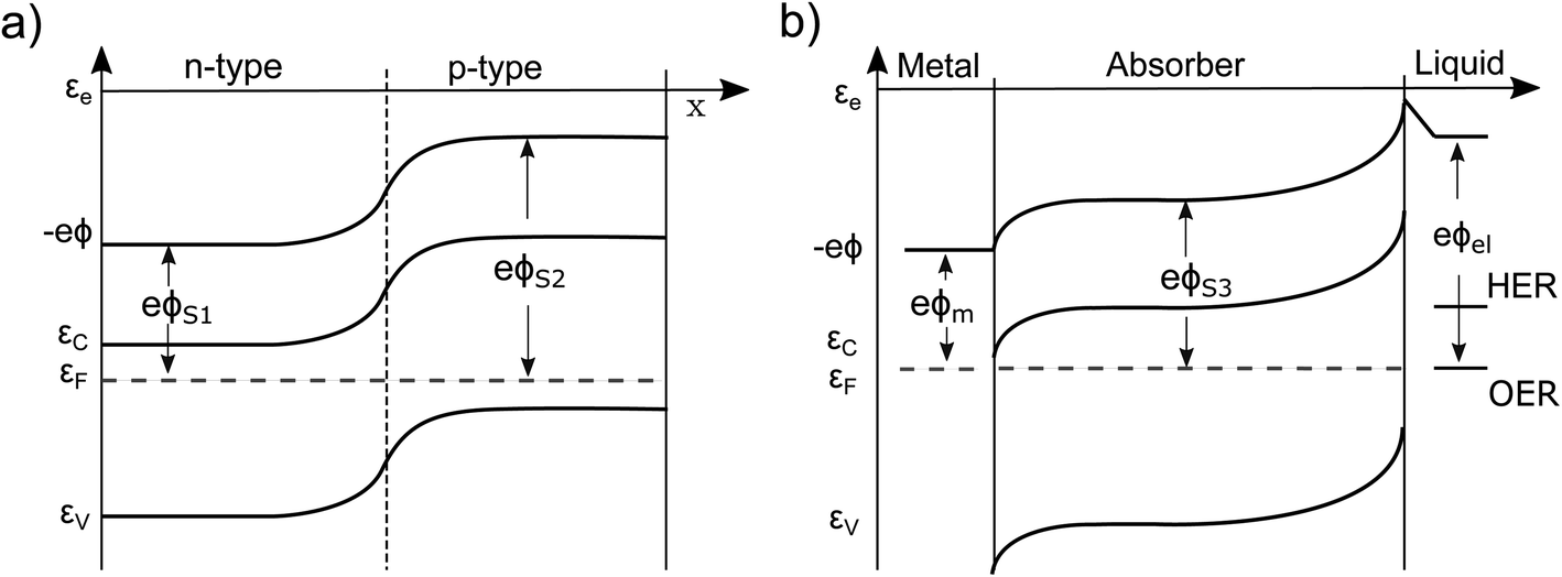 | ||
| Fig. 1 (a) A typical pn-junction in the dark. The band-bending has its origin in the diffusion of electrons from the n-doped into the p-doped region. (b) A semiconductor immersed in an electrolyte. Ideally, the Fermi level of the n-doped semiconductor aligns with the redox level of the most active species (depending on pH). A space-charge region is formed. −eϕ, EC/V, EF, eϕS1−3,m,el are the electric potential energy (typically referred to as vacuum level), the conduction/valance band energy, the Fermi energy and the material work functions, respectively. HER/OER are the hydrogen/oxygen evolution reaction redox potentials. | ||
B Excess carrier generation, free energy extraction and charge carrier transport
A solar cell converts radiant energy into electrical energy by the absorption of photons leading to the generation of free electron hole pairs and a subsequent extraction of the charge carriers. In general, the amount of energy in a solar cell that can actually perform work is considered as the Helmholtz free energy F, given by the inner energy, U, minus the product of temperature T and entropy, S.| F = U − TS. | (1) |
The exchange of free energy dF is carried out by the removal of dNe,h electrons or holes. In the steady-state operation mode (for continuous illumination) of a PV/PEC cell, the volume occupied by the charge carriers and the temperature is constant. Therefore, only chemical and electrical energy is exchanged. Further, equal amounts of electrons and holes are removed. In a semiconductor the chemical potential, μ, and the electrical potential, eϕ, are fundamentally coupled since every change in charge is associated with a change in the number of electrons and holes. Therefore, only chemical and electrical energy are exchanged, which leads to a change in free energy given by
| (μi + zieϕ)dNi = ηidNi | (2) |
Here, μi is the chemical potential of species i, zi is the electrical charge, ϕ is the electrical potential, and η is the electrochemical potential, with the subscript i referring to either electrons (e) or holes (h). Electrons and holes are added or removed in equal numbers during excitation, recombination and charge extraction. Any change in free energy by carrier extraction is thus the sum of the electrochemical potentials of the exchanged charge carriers and can be further identified with the difference in the quasi Fermi levels (QFLs), of the electrons (εFC) and holes (εFV)
| dF = dFe + dFh = (ηe + ηh)dN = (εFC − εFV)dN. | (3) |
QFLs are commonly used to describe the carrier population that is present in a semiconductor after photoexcitation and subsequent thermalization towards the respective band edge. The quasi Fermi level splitting (QFLS) in the bulk (εFC − εFV) represents the maximum possible extractable energy per charge-carrier, which must be collected before the carriers reach final equilibrium by relaxation.14,27
An important consequence of the fact that there is only one electrochemical potential for each charge carrier in a material is the existence of only one driving force for carrier transport, given by the gradient of the electrochemical potential. It describes the general case in which both an E-field (∇ϕ) and/or a concentration gradient (∇μe,h) can be present and interdependent. Thus, only one physical current density (jQ;e,h) for the respective charge carriers exists. It can be expressed by using the conductivity, σe,h, and ze,h (which is −1 for electrons, +1 for holes):
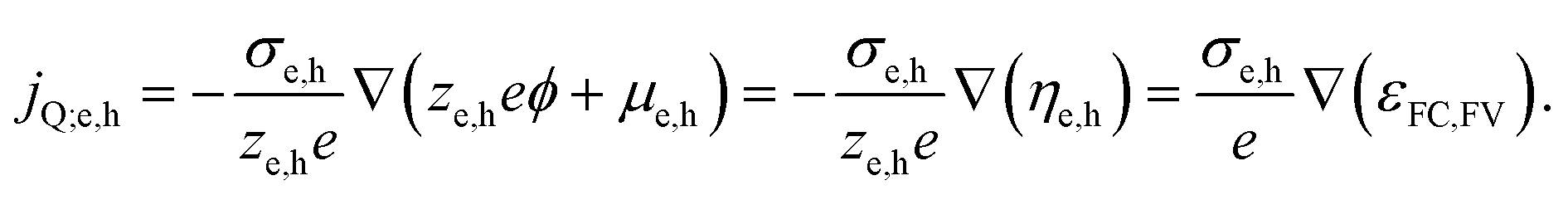 | (4) |
A simple example to analyze this principle is the case of an equilibrated pn-junction in the dark (illustrated in Fig. 1a). There is clearly a gradient in the electrical potential (∇ϕ ≠ 0), but at the same time there is a gradient in the chemical potential in opposite direction and of the same magnitude (e∇ϕ = −∇μe,h). This leads to ∇ηi = 0, i.e. a flat Fermi level and no net driving force for the charge-carriers. In this sense the built-in potential Vbi can be understood as byproduct of connecting two materials with different chemical potentials. Equilibration follows by charge carrier exchange, building up the field to compensate for this initial difference.15 This is of course equally true for the solid–liquid junction in dark equilibrium pictured in Fig. 1b.
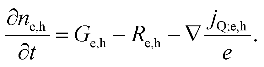
Next we take a look at the continuity equations, which relate the changes of the charge carrier densities with time 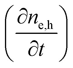 at any point in the device to the respective carrier- in and out flow (∇jQ;e,h), generation (Ge,h) and recombination (Re,h)
 | (5) |
In steady state operation  , the free carrier generation is given by the absorption of photons, while Ri is determined by Shockley–Read–Hall (SRH) recombination, radiative recombination and Auger recombination and their respective rates.28 The relationship between the net charge density and the electrical potential, is given by Poisson's law:
 | (6) |
Here ε is the permittivity and ρ is the net charge density, including free charge carriers as well as charged dopants, recombination centers, and traps. Eqn (4)–(6) represent a set of coupled partial non-linear differential equations which can be solved with appropriate boundary conditions numerically for PV and PEC devices.29–32 By this, one finally obtains the J–V characteristics of any given “classical” device. Analytical solutions are accessible for certain situations, e.g. for an idealized pn-junction leading to the well-known diode equations.14,27 Since a current needs to be extracted from a solar cell, charge carriers must be exchanged at the contacts. Therefore, surface recombination plays a critical role and is briefly discussed.
| Rs,e = SR,ene | (7) |
 | ||
| Fig. 2 (a) Interface of an unpassivated semiconductor–metal contact. Surface states are illustrated by horizontal dashes. Fast recombination leads to a coinciding of the (bulk) QFLS. (b) pn-junction under homogeneous illumination under conditions close to the maximum power point (i.e., neither short nor open circuit). Fermi level gradients are exaggerated to demonstrate the principle, also note the merging of εFC and εFV at the metal contacts. Principle adapted from ref. 14. | ||
C A pn-junction under working conditions
The free energy per electron–hole pair (V × e), that can be extracted from a device, is given by the difference in the Fermi levels at the surface contacts (εFC, left sc, εFV,right sc)13,14,18
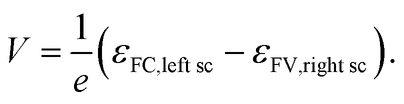 | (8) |
The electron and hole currents are at every point driven through the device by gradients of the QFLs. The main voltage losses as visible from ∇εFC,FV(x) appear in the bulk or at the contacts, as a consequence of series resistances and/or recombination. Depending on the charge carrier type and its spatial position, the current flow is dominated by drift or diffusion.
 exist. LDrift and LDiff are both a function of the mobility lifetime product (μτ) and determine how far (minority) charge carriers can travel before they recombine. The square root-dependence of the diffusion length implies LDiff < LDrift for reasonably large μτ products (that are always needed for a substantial collection efficiency) and henceforth a large depletion region is beneficial for the efficiency of many device structures.22,25 However, one should bear in mind that charge transport strongly depending on a large built-in field would often lead to a loss in fill factor (FF), since at the MPP, Vint is significantly smaller than at Isc. Furthermore, a large depletion volume is not universally helpful to achieve high efficiencies, since SRH recombination is generally larger in depleted areas (as ne ≈ nh). Therefore, large depletion areas should be avoided, if the diffusion length is sufficient for adequate charge transport.22 Prominent examples for which the absorber layer is mainly depleted are thin film technologies such as a-Si,36 CdTe,37 organic PV38,39 and ultra-thin film solar cells.40 Well-known devices which are almost entirely field free are c-Si cells,14 halide perovskites solar cells (PSCs)41 and DSSC's.23 It can be safely assumed that the picture is equally diverse for PEC water splitting devices, since they are based on very different absorber materials and cell designs. For metal oxides we expect built-in fields to play a large role for the charge transport since μτ-products are known to be small.4
D Selective contacts as fundamental working principle
If we take a step back from the specifics of the pn-junction, we can identify the necessary perquisites for a working PV device.13,47 Needed is electron–hole pair generation by photoexcitation (i) an excited state with a sufficient lifetime (ii) and two distinct terminals, each one accepting only one charge carrier type (iii) as is pictured in Fig. 3a. The pn-junction realizes these terminals by doping, which leads to an asymmetry in electron and hole conductivities. At the left-hand contact predominately electrons are extracted since these are the majority carriers in the n-type region and their conductivity and concentration is high. In the p-type region on the other hand, the holes are selectively extracted at the contact for the same reason. The junction in between the layers collects the respective minority carriers. In this way, the n- and p-doped areas can be understood as being sandwiched between two so-called selective contacts. The principle on how these contacts facilitate charge separation, might be best understood in analogy to two gases separated by semipermeable membranes,14 illustrated in Fig. 3b. The middle chamber is fed by a constant inflow of H2 and O2, which is analogous to photogeneration of new electron hole pairs within the absorber. This leads to an increase in partial pressure, that drives out the gases towards the neighboring chambers. The semipermeable membranes on both sides, in analogy to the contacts of a solar cell, facilitate the separation by letting through one molecule, but rejecting the other. | ||
| Fig. 3 (a) The three main preconditions for successful solar energy conversion: (i) photoexcitation, (ii) an exited state with a sufficient lifetime that allows for effective charge transport (drift or diffusion) (iii) two selective contacts.47 (b) Principle of semipermeable membranes separating H2 and O2. The different partial pressures between the chambers, increased by pumping of additional H2 and O2 (similar to the absorption of new photons in the solar cell), allows to separate the gases, if two semipermeable membranes are present. As long as the partial pressure of the gases in the middle is higher than in the outer compartments, the pressure gradient results in a driving force that separates the gases.14 | ||
III The toolbox for selective contact design in PV and PEC cells
In the following, we will provide some examples of how contacts of PV and PEC cells can be designed. We briefly look at the effect of doping, as well as at different types of heterostructures including so-called semi reflective-, transport-, blocking-, dipole- and passivation layers, and at tunnel junctions. To start with, Schottky barrier-, ohmic- and solid/liquid-junctions are discussed in more detail since the latter are considered to be most relevant for PEC devices.A Semiconductor/metal interface – Schottky and ohmic junctions
An idealized semiconductor/metal interface can be fully described by the work function of the metal, ϕm, the work function of the semiconductor, ϕs, and its electron affinity, χ. Let us first look at the case ϕs < ϕm in an n-doped semiconductor as depicted in Fig. 4a. After contact, the semiconductor Fermi energy equalizes itself to the Fermi level in the metal, as a finite number of electrons flow from the semiconductor into the metal. This results in a band-bending and a barrier of the height ϕB = ϕm − χs. Such a Schottky contact shows the well-known diode-like rectifying current–voltage (CV) behavior due to the space-charge region, which is depleted of majority carriers.50,51 The situation is different if ϕs > ϕm, pictured for an n-doped semiconductor in Fig. 4b. Now electrons from the metal occupy lower states within the semiconductor, again the Fermi levels align. Such a contact has now a resulting CV characteristic that is comparable to an ohmic resistor and is therefore named ohmic contact.52 Analogous alignment takes place in a p-doped semiconductor for ϕs < ϕm and ϕs > ϕm, as pictured in Fig. 4c and d. Again, a rectifying and an ohmic contact can be created. Therefore, one can build a PV device, regardless of the absorber doping, by simply using two different metals as contacts. The difference of the two metal work functions, together with the band gap of the semiconductor, limit the extractable photovoltage of such a device, which is called Schottky junction solar cell. | ||
| Fig. 4 Four types of idealized semiconductor/metal junctions. (a) Rectifying contact based on a n-doped semiconductor. (b) Ohmic contact based on a p-doped semiconductor. (c) Ohmic contact based on a n-doped semiconductor. (d) Rectifying contact based on a p-doped semiconductor. Note that the accumulation regions of ohmic contacts (b and c) are typically thinner than the depletion regions for Schottky contacts (a and d). | ||
The contact selectivity in a Schottky solar cell can be understood from the symmetry between Fig. 4a and c compared to Fig. 4b and d. The same band-bending, which leads to a rectifying behavior for the majority carriers, is ohmic for the minority carriers and vice versa, simply because the band-bending is associated with a depletion or accumulation of electrons or holes. Although in principle, the preparation of Schottky contacts should be easy, this is not the case due to the intricacies arising from the atomistic properties of the metal/semiconductor interface. The above discussion was on idealized metal/semiconductor junctions, but several effects lead to imperfect contacts. One reason is the so-called Schottky effect, an unavoidable image-force induced lowering of the potential barrier. Even more important are surface- or interface states. If the number of interface states, Dit, between the metal and the semiconductor approaches infinity (Dit → ∞), the barrier height ϕB becomes completely independent of the metal work function.50 This is called Fermi level pinning. Surface states may even lead to the formation of ohmic junctions when one would expect at first a Schottky junction to form, as it was shown for n-Si and WO3 junctions.53 That underlines that minimizing surface states is key when it comes to the preparation of Schottky contacts. In practice, however, the necessary exchange of minority carriers across a Schottky barrier almost always leads to a high level of surface recombination since a sufficient number of majority carriers remains present in the depleted region. In fact it turned out that some “well-working Schottky contacts” had actually been unintended pn-heterojunctions. This happened e.g. at the Cu contact of n-doped CdS, where p-doped Cu2S was formed.14 We will later point out similar effects at the semiconductor/electrolyte interface. Instead of a metal contact, transparent, conductive oxides (TCO's), such as fluorine-doped tin oxide (FTO) or indium tin oxide (ITO), are regularly used.54,55 Alternatively, so-called metal–insulator–semiconductor- (MIS-) junctions can be created.56,57 The insulator layer helps to passivate defects and thus to reduce recombination, while the majority carrier current flows effectively via tunneling. The two latter approaches already represent more elaborate (hetero-)contact designs addressing the shortcomings of “normal” Schottky contacts.
B Semiconductor/liquid interface – quasi-Schottky and quasi-ohmic junctions
The basics for understanding the semiconductor/liquid interface were laid out by Gerischer. Already in 1966, he recognized that the redox potential ηel in an electrolyte is analogous to the Fermi level in a semiconductor.58–60 The electronically accessible energy levels of the redox system (DOSRed/Ox) are given by two Gaussian distributions, one for the oxidized and one for the reduced component of the redox couple. The effective redox level (i.e., the ‘Fermi’ level of the solution) lies in between both, generally close to where the DOSRed/Ox of the two components is equal. If a semiconductor is placed into the electrolyte, equilibrium formation immediately demands the electrochemical potentials to equilibrate and a junction is formed. The change in electric potential necessary can drop either over the semiconductor or over the Helmholtz double layer (HHL), a several Å thin layer of (specifically) adsorbed constituents of the electrolyte. For an idealized semiconductor/electrolyte contact, one can assume the drop of voltage over the HHL to be small, and therefore the dominant part of the contact potential difference drops across the semiconductor. For highly doped semiconductors, however, most of the drop falls across the HHL, as it does for metal electrodes. It was demonstrated that the dark CV characteristic of such a junction behaves similarly to a Schottky contact.59 Still, we must note that having an electrochemical potential in an electrolyte does not mean that a free electron gas is formed. Charge transfer processes within the electrolyte are instead connected to chemical reactions or charge reorganization of the ions in the solution, which are typically many orders of magnitude slower than purely electronic processes. Nonetheless, the solid/electrolyte interface features depletion of majority carriers in the semiconductor and shows rectifying behavior. Thus, we understand it to be selective in a similar way as a Schottky contact. The depleted semiconductor/electrolyte interface is able to act as a selective contact for holes (photoanode) or electrons (photocathode) in a PEC cell. It is also possible to design a solid/liquid contact to be “ohmic”, as done for buried-junction PEC cells.7 Photoanodes and photocathodes in water splitting PEC (half) cells are based on semiconductor/liquid junctions, but it is still unclear how selective these junctions are. Conventional Schottky contacts, as commonly prepared in the lab, are known to be very problematic selective contacts, due to multiple interface states and a typically high level of surface recombination. We expect the challenges to be generally similar for quasi-Schottky contacts that form at semiconductor/electrolyte interface. In the presence of an electrolyte, multiple species might be desorbed, adsorbed or surface reconstruction and (photo)corrosion can take place. All of this potentially leads to multiple surface states. On one hand, certain surface states can be needed for catalysis since they serve as reaction intermediates (as e.g. described for Fe2O3 (ref. 61)) for the water splitting (half) reaction. On the other hand, they can be harmful for the device performance since they represent potential recombination centers for the electrons and holes. To prevent recombination, only one carrier type should be present at the surface and irreversible trapping of these carriers in surface states should be avoided. Interestingly, some solid/liquid interfaces show photo- or potential-induced corrosion that is actually helpful in this regard. One prominent example is the intentional photocorrosion of p-doped InP,62 leading to a buried pn-junction in analogy to the above-discussed Cu contact of n-doped CdS. For other cell designs additional “catalyst” layers were shown to be predominantly inhibitors of surface recombination rather than significantly influencing the charge transfer kinetics.63,64 Yet the latter examples show already a modification of the contact and should better not be considered as prime examples of the original solid/liquid junction according to Gerischer's description.C Doping
The best-known example of how doping can be used to create selective contacts is the pn-homo-junction already discussed in section IIC. A common way for further improvement is the so-called p-i-n structure. Here an intrinsic or weakly doped absorber is sandwiched between two highly doped contact layers.14,18 In the highly doped n- and p-layers, the concentration of the minority carriers is very small, while the opposite is true for the majority carriers. This reduces recombination and strongly increases the conductivity for the majority carriers. This principle has also been used in photoelectrochemical devices. One example is a p-i-n structure created in a hematite photoanode, which led to a significant improvement of the photocurrent and the onset potential.65 Also, gradient doping is feasible.55,66–68 In 2013, Abdi et al. achieved 4.9% STH eff. for a metal oxide-based, stand-alone solar water splitting device, based on a photoanode from BiVO4 in a tandem configuration with c-Si.55 Key element was the introduction of an n-type doping gradient in W-doped BiVO4, which helped to improve charge separation.D Heterostructures: transport and blocking layers, window layers, dipole layers and tunnel junctions
Conventional heterostructures are made by combining two semiconductors with different electron affinities and/or band gaps, allowing to design band offsets. If also the work functions of the semiconductor (which can be manipulated by doping) differ, band bending is introduced, analogous to the case of pn-homojunctions. One example of such a pn-heterojunction is CdS-coated CuGaSe2, where the CdS “buffer” layer acts as an electron selective or hole blocking layer and facilities charge separation by appropriate band alignment. Although such a system has been widely investigated for thin film PV applications, it has also been implemented as a photocathode for PEC water splitting.69 However, next to typical semiconductors also other materials are feasible, as detailed below. To construct a well-functioning heterojunction, in terms of charge selectivity, one must use a material which provides an energetically favorable pathway for one type of charge carrier, while blocking the other type with a potential barrier. These layers are often referred to as hole blocking/electron transport layers (ETL) or electron blocking/hole transport layers (HTL) as illustrated in Fig. 5b. Other terminology can also be used to cover the function of the transport layer, these include “buffer layer” or “inter layer” and when transparent to the incident illumination the term “window layer” is also used. | ||
| Fig. 5 Band diagrams of PEC devices under homogeneous illumination: (a) n-doped absorber layer with a metal back- and a liquid front contact. Surface recombination leads to voltage losses, therefore the extractable energy per electron hole pair ΔεNOSCF is significantly smaller than ΔεmaxF. For water-splitting, an additional bias voltage would be necessary. (b) Weakly doped absorber sandwiched between two additional contact layers added for optimization. The voltage losses are significantly smaller, therefore the extracted free energy ΔεOSCF is closer to ΔεmaxF. Furthermore, an additional catalyst (in green) is added to minimize the overpotentials, necessary to run the reaction. | ||
Transport layers can be composed of inorganic materials, including metal oxides (e.g. ETL: SnO2, TiO2, ZnO, In2O3, Ga2O3, and HTL: MoOx, V2Ox, NiOx), metal chalcogenides (e.g. ETL: CdS, Zn(O,S), ZnS, ZnSe, and HTL: CuInS2, CuS), metal pnictides (e.g. ETL: AlInP), metal halides (e.g. ETL: LiF, HTL: CuI), or metal–organic coordination polymers (e.g. HTL: CuSCN), as well as, organic materials such as charge selective polymers (e.g. HTL: poly-3,4-ethylenedioxythiophene (PEDOT:PSS), poly[bis(4-phenyl)(2,4,6-trimethylphenyl)amine] (PTAA)), functionalised carbonaceous materials (e.g. ETL: fullerene, phenyl-C61-butyric acid methyl ester (PCBM), and HTL: graphene oxide, 2,2′,7,7′-tetrakis [N,N-di(4-methoxyphenyl)amino]-9,9′-spirobifluorene (spiro-OMeTAD)) or by functionalising the absorber surfaces with a molecular monolayer. Depending on certain factors, such as the fabrication parameters (particularly temperature), surface chemistries and the lattice alignment the resluting energy levels and work functions may differ drasstically. This results in a diverse array of transport layers that can be interchangeable and combined to act as ETLs and HTLs for different absorber types, and are crucial for optimising cell performance. As an example, the n-type AlInP/AlInPOx is an inorganic ETL that was recently optimised for the record III–V based PEC device.8 For p-type CuBi2O4 photocathodes, is was found that there is a significantly improved photon-to-current efficiency when using a Cu:NiOx electron blocking underlayer.70 One promising approach to form efficient charge selectivity is to functionalize the surface of the absorber with self-assembled monolayers (SAMs) of which some possess large dipoles. The adsorbed (dipolar) molecules modify the work function of the absorber surface creating an energetic barrier for a certain carrier type. Since the transport layer is effectively a single monolayer, the ohmic losses are minimized. This is sufficiently effective for efficient absorber materials which possess high carrier diffusion lengths and do not require large electric fields to assist in charge transport. SAMs have therefore been utilised to optimise the performance of PSCs71 and act as highly efficient molecular scale transport layers.72 Also tunnel junctions have proven to be a very efficient contact principle,8,10 here a wide-band gap layer is deposited thin enough to passivate defects, but still allow a significant majority carrier tunnel current. Another example of a successful combination of both doping and heterostructure design is given by a photocathode realized using p-i-n doped a-Si sandwiched between ZnO and TiO2 contact layers.73 A more detailed description of different heterostructures possible is found elsewhere.19,74
E Further approaches: mobility junctions, reaction kinetics, and energy-selective contacts
Some other approaches that do not fit directly into the scheme of homo- and heterojunctions should be mentioned. An interesting concept is the so-called ‘mobility junction’, in which a material with a high electron mobility (and low hole mobility) is contacted with a material with a high hole mobility (and low electron mobility). Such devices are expected to show high charge separation efficiencies.13 Efficient carrier separation also plays a key role in natural75–77 and artificial78 photosynthetic water splitting processes. Here, carrier selectivity is realized by offering distinct kinetically favored reaction pathways that enable the spatial separation of the carriers. Such favorable reaction pathways can also play an important role for certain semiconductor/electrolyte interfaces.79 A notable third generation approach is the so-called hot carrier solar cell (HC-SC),80–84 here the carriers must not only be spatially separated, but also collected in a narrow energy range using energy-selective contacts. This avoids thermalization losses85 and can be achieved with resonant tunnelling structures84 with phononic band gaps,86 which allow for long phonon lifetimes. The latter approach could, in principle, also be used for the construction of hot carrier photoelectrochemical water splitting devices.F Applied bias
Semiconductor photoanodes and cathodes are often investigated under an externally applied bias potential. A reverse bias leads to a wider depletion layer and a lower concentration of majority carriers at the interface.4 It is especially the latter effect that leads to a higher selectivity, as discussed above. In addition, the drift current density increases throughout the absorber as described in paragraph IIC2 and modelled in the literature (mostly for the examples of pin-junctions, in which a widespread depletion is apparent).15,22,27,87 Thus, the applied bias is increasing the collection efficiency by accelerating the transport and also reducing recombination losses by improving the selectivity at the interface. Still, one should not consider additional bias to be a reasonable pathway towards contact optimization. It obviously comes at the cost of an additional free energy loss that could hardly be afforded in an optimized standalone device. We will further discuss this in paragraph IV.G Summarizing the toolbox
All the above-mentioned considerations, including doping and heterostructure designs help to enable or improve contact selectivity in one way or another. Often one would use multiple effects in one layer or combine them by adding further components. It is also important to realize that any carefully designed and optimized interface may change due to surface oxidation and/or reconstruction upon simple exposure to air or electrolytes, under illumination, or under applied potential in an electrochemical system.88 Yet one must consider that even low concentrations of adsorbates or dissolved molecules can impact the surface work function. This may even lead to the dissolution of functional layers, or the formation of new interlayers. Clearly, such effects can be (and usually are) very harmful for the contact and the overall device operation. To qualitatively evaluate the potential improvements by contact optimization, we will compare a “conventional” PEC cell to one with optimized contacts using some of the tools described above in the next section.IV The “conventional” vs. the “optimal” PEC cell
A The “conventional” PEC cell
Finally, we turn our attention to a complete photoelectrochemical cell. In Fig. 5a, a wide-band gap absorber under homogeneous illumination is displayed (the same absorber in the dark is depicted in Fig. 1b). It has a metal contact on the left and an electrolyte contact on the right. We assume the absorber to be an n-doped photoanode and therefore the left contact is ohmic for the electrons. The gradient in εFC drives the electrons towards the left contact and it does so at the cost of some photovoltage. At the same time, also some holes are driven towards the contact due to surface recombination, but since they are minority carriers, the Fermi levels join closer to the conduction band. Analogous behavior is observed at the semiconductor/electrolyte contact. This time, due to the depletion of electrons and the accumulation of holes in the space-charge region, mainly holes reach the surface. The quasi Fermi levels bend towards the surface, depending on the magnitude of the surface recombination velocity (and would even join for a very high level of surface recombination within a certain state as present e.g. in a metal catalyst). The gradient in hole QFL εFV reflects transport and surface recombination losses that reduces the Gibbs free energy (ΔG) that can be finally delivered to drive the chemical reaction. The band bending at the illuminated solid/liquid interface is reduced by the amount of photovoltage delivered (in comparison to the case in the dark pictured in Fig. 1b). The illustrated device with non-optimized selective contacts (NOSC) delivers not enough free energy to split water and there is a significant loss compared to available free energy as denoted by the bulk QFLS (ΔεNOSCF < 1.23 eV < ΔεmaxF). Such devices are often investigated with an additional bias potential that is applied to determine the point at which the water splitting reaction is more favorable than the back reaction (VBias + Voc) and to determine how much current could be delivered. The bias potential (that will also increase the space charge region) can originate from a potentiostat or from an additional solar cell (tandem device). A detailed description and a numerical modeling of the transport processes that occur at the Schottky and quasi Schottky contacts can be found in the work of Iqbal and Bevan.30 Electron and hole current continuity equations are solved simultaneously to capture both photocurrent and photovoltage. The VB, CB and QFLs align according to the numerical model as described by us qualitatively. The only difference is that there is no bending of the electron QFL (εFC) towards the liquid surface. This is because the electron transfer velocity towards the liquid is deliberately set to zero throughout the simulation. Such optimized surface contact is an assumption that generally cannot be made.B The “optimal” PEC cell
In Fig. 5b an improved configuration is sketched. The weakly doped absorber is sandwiched by two doped layers forming (buried) heterojunctions, which act as both selective contact and as capacitive element of the PEC cell. The back contact has a band alignment that does not allow holes to pass, furthermore it is strongly n-doped assuring a high electron conductivity. Thus, the voltage- and carrier-loss at the junction are minimized. At the front contact on the other side, the electrons are blocked, while the holes move with low resistance due to the high p-doping towards the electrolyte. The resulting voltage loss by surface recombination is likely to be significantly smaller. In such a configuration, the back contact is the photocathode and the front contact the photoanode. The delivered free energy per electron–hole pair is higher due to an optimized selectivity of the contacts (OSC) and close to the bulk maximum. In the sketched p-i-n structure the band bending appears only close to the contacts, since in an optimized device the αμτ-product should be large enough to ensure efficient transport by diffusion alone. Otherwise one could switch to an intrinsic absorber. Then the voltage drop would be more continuous over the absorber.22 We note that, although the contacts are sketched to be symmetric in Fig. 5, this does not have to be the case. The voltage loss at one contact can be significantly higher than at the other.It is instructive to see that the course of the electrochemical potential for the holes, in case of the conventional device (illustrated in Fig. 5a), is running nearly in parallel to the band-bending at the right hand contact. This is in full agreement with the intuitive picture of charge carrier separation driven by a built-in electrical field. Although this gradient indeed reflects a driving force, the energy needed for the transport of the charges has its origin in the electrochemical potential of the electron–hole pair, thus originating from the photon energy itself and not from the internal E-field. Therefore, one always has a trade-off between efficient charge delivery (current) and extracted energy per electron–hole-pair (voltage). This is indeed well-known also for a classical PV cell. The maximum current Isc cannot be reached at Voc. To get a high fill factor, it is desirable to minimize the gradient in Fermi level that is needed for charge transport and separation to finally obtain a maximum voltage. Similarly we can understand the reaction kinetics in the PEC cell. If the kinetics, for example for the OER, are too slow, this must be compensated by a higher overpotential. A high-performance catalyst, pictured in green in Fig. 5, is most likely to be needed for an optimal PEC cell and can minimize this loss mechanism.18 Detailed numerical modelling of p-i-n structures that backs up our qualitative descriptions has been performed multiple times: we find especially the work in ref. 15, 22 and 27 very instructive. We refrain here form our own modeling since the performance of any structure would simply depend on the input parameters, which are for novel absorber/contact layers typically not known, yet.
V Summary
To summarize, we argued that, just like in a PV cell, the only driving force for charge separation in a PEC device is the gradient of the electrochemical potential. The built-in E-field in the junction, predominantly present in the dark, is not in general sufficient to explain the direction of current flow, although it facilities charge transport in many device structures. Most importantly the built-in field serves as a capacitive element that allows a photovoltage to develop. We find the contact selectivity to be a key guiding principle for the design of efficient devices and several advanced approaches to construct highly selective contacts were discussed. We further described a complete PEC device qualitatively and identified several possibilities for optimization. Current and voltage losses can be reduced in bulk by maximizing the αμτ product and losses at the contact can be minimized by ensuring a high charge carrier selectivity. All loss mechanisms are visible as gradients of the quasi Fermi levels, their maximum splitting corresponds to the maximum free energy available to drive the electrochemical reactions. This illustrates the importance of knowing the position of the quasi Fermi levels at every point in the device. Moreover, it suggests that quantum efficiency and photocurrent measurements, while useful, only tell part of the story. To achieve high fill factors and high STH efficiencies, charge transport should be efficient even in the absence of either internal or externally applied electric fields. We hope that this work contributes to a better understanding of the processes underlying charge transport and separation in PEC devices and to shift the attention of the community from “idealized” and “conventional” solid–liquid junctions towards a more general concept of selective contacts that are needed to construct an efficient PEC device for solar energy conversion.Conflicts of interest
There are no conflicts to declare.Acknowledgements
MM acknowledges funding from the German Research Foundation (DFG), Project No. 434023472 and the Volkswagen Foundation, RvdK acknowledge financial support from the DFG for project PAK-981. Part of this research was carried out within the Helmholtz International Research School “Hybrid Integrated Systems for Conversion of Solar Energy” (HI-SCORE), an initiative co-funded by the Initiative and Networking Fund of the Helmholtz Association. M. S. specifically thanks Klaus Schwarzburg, Hannes Hempel, Peter Bogdanoff, Raphael Präg, Patrick Schnell from HZB, as well as J. F. Guillemoles, Thomas Kirchartz, Uwe Rau, Tom Markvart and Peter Würfel for inspiring discussions. Further, M. S. thanks particularly Avner Rothschild for reading and commenting on the manuscript.References
- D. K. Dogutan and D. G. Nocera, Artificial photosynthesis at efficiencies greatly exceeding that of natural photosynthesis, Acc. Chem. Res., 2019, 52, 3143–3148 CrossRef CAS PubMed.
- J. A. Turner, Sustainable hydrogen production, Science, 2004, 305, 972–974 CrossRef CAS PubMed.
- B. Parkinson and J. Turner, The potential contribution of photoelectrochemistry in the global energy future, in Photoelectrochemical Water Splitting: Materials, Processes and Architectures, ed H.-J. Lewerenz and L. Peter, The Royal Society of Chemistry, 2013, ch. 1, pp. 1–18 Search PubMed.
- R. van de Krol and M. Grätzel, Electronic Materials: Science & Technology, Springer, New York Dordrecht Heidelberg London, 2012, p. 321 Search PubMed.
- R. van de Krol and B. A. Parkinson, Perspectives on the photoelectrochemical storage of solar energy, MRS Energy Sustain., 2017, 4, E13 CrossRef.
- M. R. Shaner, H. A. Atwater, N. S. Lewis and E. W. McFarland, A comparative technoeconomic analysis of renewable hydrogen production using solar energy, Energy Environ. Sci., 2016, 9, 2354–2371 RSC.
- W.-H. Cheng, M. H. Richter, M. M. May, J. Ohlmann, D. Lackner, F. Dimroth, T. Hannappel, H. A. Atwater and H.-J. Lewerenz, Monolithic Photoelectrochemical Device for 19% Direct Water Splitting, ACS Energy Lett., 2018, 3, 1795–1800 CrossRef CAS.
- M. M. May, H.-J. Lewerenz, D. Lackner, F. Dimroth and T. Hannappel, Efficient Direct Solar-to-Hydrogen Conversion by In Situ Interface Transformation of a Tandem Structure, Nat. Commun., 2015, 6, 8286 CrossRef CAS PubMed.
- M. M. May, H. Döscher, and J. Turner, High-efficiency water splitting systems, in Integrated Solar Fuel Generators, Energy and Environment Series, ed I. D. Sharp, H. A. Atwater, and H.-J. Lewerenz, The Royal Society of Chemistry, 2018, ch. 12, pp. 454–499 Search PubMed.
- J. L. Young, M. A. Steiner, H. Döscher, R. M. France, J. A. Turner and T. G. Deutsch, Direct solar-to-hydrogen conversion via inverted metamorphic multi-junction semiconductor architectures, Nat. Energy, 2017, 2, 17028 CrossRef CAS.
- Y. Zhang, H. Lv, Z. Zhang, L. Wang, X. Wu and H. Xu, Stable unbiased photo-electrochemical overall water splitting exceeding 3% efficiency via covalent triazine framework/metal oxide hybrid photoelectrodes, Adv. Mater., 2021, 33, 2008264 CrossRef CAS PubMed.
- L. Pan, J. H. Kim, M. T. Mayer, M.-K. Son, A. Ummadisingu, J. S. Lee, A. Hagfeldt, J. Luo and M. Grätzel, Boosting the performance of Cu2O photocathodes for unassisted solar water splitting devices, Nat. Catal., 2018, 1, 412–420 CrossRef CAS.
- U. Würfel, A. Cuevas and P. Würfel, Charge carrier separation in solar cells, IEEE J. Photovoltaics, 2015, 5, 461–469 Search PubMed.
- P. Würfel and U. Würfel, Physics of Solar Cells: From Basic Principles to Advanced Concepts, John Wiley and Sons, 2009 Search PubMed.
- U. Rau and T. Kirchartz, Charge Carrier Collection and Contact Selectivity in Solar Cells, Adv. Mater. Interfaces, 2019, 6(20), 1900252 CrossRef CAS.
- A. Onno, C. Chen, P. Koswatta, M. Boccard and Z. C. Holman, Passivation, conductivity, and selectivity in solar cell contacts: Concepts and simulations based on a unified partial-resistances framework, J. Appl. Phys., 2019, 126, 183103 CrossRef.
- Z. Zhang and J. T. Yates, Band bending in semiconductors: Chemical and physical consequences at surfaces and interfaces, Chem. Rev., 2012, 112, 5520–5551 CrossRef CAS PubMed.
- W. Jaegermann, B. Kaiser, F. Finger, V. Smirnov and R. Schäfer, Design considerations of efficient photo-electrosynthetic cells and its realization using buried junction si thin film multi absorber cells, Z. Phys. Chem., 2020, 234, 549–604 CrossRef CAS.
- E. L. Ratcliff, B. Zacher and N. R. Armstrong, Selective interlayers and contacts in organic photovoltaic cells, J. Phys. Chem. Lett., 2011, 2, 1337–1350 CrossRef CAS PubMed.
- M. G. Walter, E. L. Warren, J. R. McKone, S. W. Boettcher, Q. Mi, E. A. Santori and N. S. Lewis, Solar water splitting cells, Chem. Rev., 2010, 110, 6446–6473 CrossRef CAS PubMed.
- W. W. Gärtner, Depletion-layer photoeffects in semiconductors, Phys. Rev., 1959, 116, 84–87 CrossRef.
- T. Kirchartz, J. Bisquert, I. Mora-Sero and G. Garcia-Belmonte, Classification of solar cells according to mechanisms of charge separation and charge collection, Phys. Chem. Chem. Phys., 2015, 17, 4007–4014 RSC.
- B. A. Gregg, Interfacial processes in the dye-sensitized solar cell, Coord. Chem. Rev., 2004, 248, 1215–1224 CrossRef CAS.
- A. J. Cowan and J. R. Durrant, Long-lived charge separated states in nanostructured semiconductor photoelectrodes for the production of solar fuels, Chem. Soc. Rev., 2013, 42, 2281–2293 RSC.
- T. Kirchartz and U. Rau, What Makes a Good Solar Cell?, Adv. Energy Mater., 2018, 8, 1703385 CrossRef.
- W. Ruppel, Photospannungen in photoleitern i. allgemeiner ausdruck, Phys. Status Solidi B, 1964, 5, 657–666 CrossRef CAS.
- S. J. Fonash, Solar Cell Device Physics, Elsevier, 2010 Search PubMed.
- W. Shockley and W. T. Read, Statistics of the recombinations of holes and electrons, Phys. Rev., 1952, 87, 835–842 CrossRef CAS.
- D. Schroeder, Boundary and interface conditions of transport equations for device simulation, in Festkörperprobleme 36, ed R. Helbig, Springer Berlin Heidelberg, Berlin, Heidelberg, 1996, pp. 265–283 Search PubMed.
- A. Iqbal and K. H. Bevan, Simultaneously Solving the Photovoltage and Photocurrent at Semiconductor-Liquid Interfaces, J. Phys. Chem. C, 2018, 122, 30–43 CrossRef CAS.
- A. Iqbal, M. S. Hossain and K. H. Bevan, The role of relative rate constants in determining surface state phenomena at semiconductor–liquid interfaces, Phys. Chem. Chem. Phys., 2016, 18, 29466–29477 RSC.
- A. Iqbal and K. H. Bevan, The impact of boundary conditions on calculated photovoltages and photocurrents at photocatalytic interfaces, MRS Commun., 2018, 8, 466–473 CrossRef CAS.
- Q. Yan, J. Yu, S. K. Suram, L. Zhou, A. Shinde, P. F. Newhouse, W. Chen, G. Li, K. A. Persson, J. M. Gregoire and J. B. Neaton, Solar fuels photoanode materials discovery by integrating high-throughput theory and experiment, Proc. Natl. Acad. Sci., 2017, 114, 3040–3043 CrossRef CAS PubMed.
- U. Rau, G. Kron and J. H. Werner, Reply to comments on “electronic transport in dye-sensitized nanoporous TiO2 solar cells comparison of electrolyte and solid-state devices” on the photovoltaic action in pn-junction and dye-sensitized solar cells, J. Phys. Chem. B, 2003, 107, 13547–13550 CrossRef CAS.
- G. Kron, U. Rau and J. H. Werner, Influence of the built-in voltage on the fill factor of dye-sensitized solar cells, J. Phys. Chem. B, 2003, 107, 13258–13261 CrossRef CAS.
- M. I. Kabir, Z. Ibarahim, K. Sopian and N. Amin, A review on progress of amorphous and microcrystalline silicon thin-film solar cells, Recent Pat. Electr. Eng., 2011, 4, 50–62 CrossRef CAS.
- I. M. Dharmadasa, A. E. Alam, A. A. Ojo and O. K. Echendu, Scientific complications and controversies noted in the field of CdS/CdTe thin film solar cells and the way forward for further development, J. Mater. Sci.: Mater. Electron., 2019, 30, 20330–20344 CrossRef CAS.
- J. Yu, Y. Zheng and J. Huang, Towards high performance organic photovoltaic cells: A review of recent development in organic photovoltaics, Polymers, 2014, 6, 2473–2509 CrossRef.
- A. Petersen, T. Kirchartz and T. A. Wagner, Charge extraction and photocurrent in organic bulk heterojunction solar cells, Phys. Rev. B, 2012, 85, 045208 CrossRef.
- Y. Wang, S. R. Kavanagh, I. Burgués-Ceballos, A. Walsh, D. O. Scanlon and G. Konstantatos, Cation disorder engineering yields AgBiS2 nanocrystals with enhanced optical absorption for efficient ultrathin solar cells, Nat. Photonics, 2022, 16, 235–241 CrossRef CAS.
- M. M. Lee, J. Teuscher, T. Miyasaka, T. N. Murakami and H. J. Snaith, Efficient hybrid solar cells based on meso-superstructured organometal halide perovskites, Science, 2012, 338, 643–647 CrossRef CAS PubMed.
- B. Lipovšek, F. Smole, M. Topič, I. Humar and A. R. Sinigoj, Driving forces and charge-carrier separation in p–n junction solar cells, AIP Adv., 2019, 9, 055026 CrossRef.
- A. Shang and X. Li, Photovoltaic Devices: Opto-Electro-Thermal Physics and Modeling, Adv. Mater., 2017, 29, 1–8 Search PubMed.
- R. Couderc, M. Amara and M. Lemiti, In-Depth Analysis of Heat Generation in Silicon Solar Cells, IEEE J. Photovoltaics, 2016, 6, 1123–1131 Search PubMed.
- R. Brendel, S. Dreissigacker, N.-P. Harder and P. P. Altermatt, Theory of analyzing free energy losses in solar cells, Appl. Phys. Lett., 2008, 93, 173503 CrossRef.
- P. Kaienburg, L. Krückemeier, D. Lübke, J. Nelson, U. Rau and T. Kirchartz, How solar cell efficiency is governed by the αμτ product, Phys. Rev. Res., 2020, 2, 023109 CrossRef CAS.
- M. A. Green, Photovoltaic principles, Phys. E, 2002, 14, 11–17 CrossRef CAS.
- E. T. Roe, K. E. Egelhofer and M. C. Lonergan, Limits of contact selectivity/recombination on the open-circuit voltage of a photovoltaic, ACS Appl. Energy Mater., 2018, 1, 1037–1046 CrossRef CAS.
- R. Brendel and R. Peibst, Contact selectivity and efficiency in crystalline silicon photovoltaics, IEEE J. Photovoltaics, 2016, 6, 1413–1420 Search PubMed.
- D. A. Neamen, Semiconductor physics and devices: basic principles, McGraw-Hill, 2012, p. 758 Search PubMed.
- K. W. Böer, Introduction to Space Charge Effects in Semiconductors, Springer, Berlin Heidelberg, 2010 Search PubMed.
- D. K. Schroder and D. L. Meier, Solar Cell Contact Resistance—A Review, IEEE Trans. Electron Devices, 1984, 31, 637–647 Search PubMed.
- I. Y. Ahmet, S. Berglund, A. Chemseddine, P. Bogdanoff, R. F. Präg, F. F. Abdi and R. van de Krol, Planar and nanostructured n-si/metal-oxide/wo3/BiVO4 monolithic tandem devices for unassisted solar water splitting, Adv. Energy Sustainability Res., 2020, 1, 2000037 CrossRef.
- A. Chen and K. Zhu, Effects of TCO work function on the performance of TCO/n-Si hetero-junction solar cells, Sol. Energy, 2014, 107, 195–201 CrossRef CAS.
- F. F. Abdi, L. Han, A. H. M. Smets, M. Zeman, B. Dam and R. van de Krol, Efficient solar water splitting by enhanced charge separation in a bismuth vanadate-silicon tandem photoelectrode, Nat. Commun., 2013, 4, 1–7 Search PubMed.
- I. A. Digdaya, B. J. Trześniewski, G. W. P. Adhyaksa, E. C. Garnett and W. A. Smith, General Considerations for Improving Photovoltage in Metal–Insulator–Semiconductor Photoanodes, J. Phys. Chem. C, 2018, 122, 5462–5471 CrossRef CAS PubMed.
- G. Loget, Water oxidation with inhomogeneous metal-silicon interfaces, Curr. Opin. Colloid Interface Sci., 2019, 39, 40–50 CrossRef CAS.
- H. Gerischer, Charge transfer processes at semiconductor-electrolyte interfaces in connection with problems of catalysis, Surf. Sci., 1969, 18, 97–122 CrossRef CAS.
- H. Gerischer, Electrochemical photo and solar cells principles and some experiments, J. Electroanal. Chem. Interfacial Electrochem., 1975, 58, 263–274 CrossRef CAS.
- G. Kreysa, K.-I. Ota, and R. Savinell, Encyclopedia of Applied Electrochemistry, 2014 Search PubMed.
- J. Li, W. Wan, C. A. Triana, H. Chen, Y. Zhao, C. K. Mavrokefalos and G. R. Patzke, Reaction kinetics and interplay of two different surface states on hematite photoanodes for water oxidation, Nat. Commun., 2021, 12, 255 CrossRef CAS PubMed.
- T. Hannappel, M. M. May, and H.-J. Lewerenz, Epitaxial III-V Thin Film Absorbers: Preparation, Efficient InP Photocathodes and Routes to High Efficiency Tandem Structures, in Photoelectrochemical Water Splitting: Materials, Processes and Architectures, Energy and Environment Series, ed H.-J. Lewerenz and L. Peter, The Royal Society of Chemistry, 2013, ch. 9, pp. 223–265 Search PubMed.
- C. Zachäus, F. F. Abdi, L. M. Peter and R. van de Krol, Photocurrent of BiVO4 is limited by surface recombination, not surface catalysis, Chem. Sci., 2017, 8, 3712–3719 RSC.
- D. K. Zhong, S. Choi and D. R. Gamelin, Near-complete suppression of surface recombination in solar photoelectrolysis by “Co-Pi” catalyst-modified W:BiVO4, J. Am. Chem. Soc., 2011, 133, 18370–18377 CrossRef CAS PubMed.
- A. Kay, D. A. Grave, D. S. Ellis, H. Dotan and A. Rothschild, Heterogeneous Doping to Improve the Performance of Thin-Film Hematite Photoanodes for Solar Water Splitting, ACS Energy Lett., 2016, 1, 827–833 CrossRef CAS.
- T. Wu, C. Zhen, H. Zhu, J. Wu, C. Jia, L. Wang, G. Liu, N. G. Park and H. M. Cheng, Gradient sn-doped heteroepitaxial film of faceted rutile TiO2 as an electron selective layer for efficient perovskite solar cells, ACS Appl. Mater. Interfaces, 2019, 11(12), 19638–19646 CrossRef CAS PubMed.
- C. L. Zhang, H. J. Du, J. Z. Zhu, T. F. Xu and X. Y. Fang, Enhanced photovoltaic properties of gradient doping solar cells, Chin. Phys. Lett., 2012, 29(12), 127305 CrossRef.
- H. J. Du, W. C. Wang, B. Ma, T. Long and J. Z. Zhu, Band structure adjustment of solar cells by gradient doping, Mater. Sci. Semicond. Process., 2015, 40, 570–577 CrossRef CAS.
- M. Moriya, T. Minegishi, H. Kumagai, M. Katayama, J. Kubota and K. Domen, Stable hydrogen evolution from cds-modified CuGaSe2 photoelectrode under visible-light irradiation, J. Am. Chem. Soc., 2013, 135, 3733–3735 CrossRef CAS PubMed.
- A. Song, P. Plate, A. Chemseddine, F. Wang, F. F. Abdi, M. Wollgarten, R. van de Krol and S. P. Berglund, Cu:nio as a hole-selective back contact to improve the photoelectrochemical performance of CuBi2O4 thin film photocathodes, J. Mater. Chem. A, 2019, 7, 9183–9194 RSC.
- R. Wick-Joliat, T. Musso, R. R. Prabhakar, J. Löckinger, S. Siol, W. Cui, L. Sévery, T. Moehl, J. Suh, J. Hutter, M. Iannuzzi and S. D. Tilley, Stable and tunable phosphonic acid dipole layer for band edge engineering of photoelectrochemical and photovoltaic heterojunction devices, Energy Environ. Sci., 2019, 12, 1901–1909 RSC.
- A. Al-Ashouri, A. Magomedov, M. Roßz, M. Jošt, M. Talaikis, G. Chistiakova, T. Bertram, J. A. Márquez, E. Köhnen, E. Kasparavičius, S. Levcenco, L. Gil-Escrig, C. J. Hages, R. Schlatmann, B. Rech, T. Malinauskas, T. Unold, C. A. Kaufmann, L. Korte, G. Niaura, V. Getautis and S. Albrecht, Conformal monolayer contacts with lossless interfaces for perovskite single junction and monolithic tandem solar cells, Energy Environ. Sci., 2019, 12, 3356–3369 RSC.
- Y. Lin, C. Battaglia, M. Boccard, M. Hettick, Z. Yu, C. Ballif, J. W. Ager and A. Javey, Amorphous Si thin film based photocathodes with high photovoltage for efficient hydrogen production, Nano Lett., 2013, 13, 5615–5618 CrossRef CAS PubMed.
- S. J. A. Moniz, S. A. Shevlin, D. J. Martin, Z.-X. Guo and J. Tang, Visible-light driven heterojunction photocatalysts for water splitting – a critical review, Energy Environ. Sci., 2015, 8, 731–759 RSC.
- M.-L. Groot, F. van Mourik, C. Eijckelhoff, I. H. M. van Stokkum, J. P. Dekker and R. van Grondelle, Charge separation in the reaction center of photosystem II studied as a function of temperature, Proc. Natl. Acad. Sci., 1997, 94, 4389–4394 CrossRef CAS PubMed.
- E. Romero, I. H. M. van Stokkum, V. I. Novoderezhkin, J. P. Dekker and R. van Grondelle, Two different charge separation pathways in photosystem II, Biochemistry, 2010, 49, 4300–4307 CrossRef CAS PubMed.
- Y. Tachibana, L. Vayssieres and J. R. Durrant, Artificial photosynthesis for solar water-splitting, Nat. Photonics, 2012, 6, 511–518 CrossRef CAS.
- K. Maeda and K. Domen, Photocatalytic water splitting: Recent progress and future challenges, J. Phys. Chem. Lett., 2010, 1, 2655–2661 CrossRef CAS.
- F. Niu, D. Wang, F. Li, Y. Liu, S. Shen and T. J. Meyer, Hybrid photoelectrochemical water splitting systems: From interface design to system assembly, Adv. Energy Mater., 2020, 10, 1900399 CrossRef.
- S. K. Shrestha, P. Aliberti and G. J. Conibeer, Energy selective contacts for hot carrier solar cells, Sol. Energy Mater. Sol. Cells, 2010, 94, 1546–1550 CrossRef CAS.
- A. L. Bris and J.-F. Guillemoles, Hot carrier solar cells: Achievable efficiency accounting for heat losses in the absorber and through contacts, Appl. Phys. Lett., 2010, 97, 113506 CrossRef.
- G. Conibeer, R. Patterson, L. Huang, J.-F. Guillemoles, D. Kőnig, S. Shrestha and M. A. Green, Modelling of hot carrier solar cell absorbers, Sol. Energy Mater. Sol. Cells, 2010, 94, 1516–1521 CrossRef CAS.
- A. Marti and A. Luque, Electrochemical potentials (quasi-fermi levels) and the operation of hot-carrier, impact-ionization, and intermediate-band solar cells, IEEE J. Photovoltaics, 2013, 3, 1298–1304 Search PubMed.
- G. J. Conibeer, D. König, M. A. Green and J. F. Guillemoles, Slowing of carrier cooling in hot carrier solar cells, Thin Solid Films, 2008, 516, 6948–6953 CrossRef CAS.
- R. Patterson, M. Kirkengen, B. P. Veettil, D. Konig, M. A. Green and G. Conibeer, Phonon lifetimes in model quantum dot superlattice systems with applications to the hot carrier solar cell, Sol. Energy Mater. Sol. Cells, 2010, 94, 1931–1935 CrossRef CAS.
- S. Chung, S. Shrestha, X. Wen, Y. Feng, N. Gupta, H. Xia, P. Yu, J. Tang and G. Conibeer, Evidence for a large phononic band gap leading to slow hot carrier thermalisation, IOP Conf. Ser.: Mater. Sci. Eng., 2014, 68, 012002 Search PubMed.
- S. Ravishankar, J. Bisquert, and T. Kirchartz, Interpretation of Mott-Schottky plots of photoanodes for water splitting, 2022, arXiv:2201.04017 [cond-mat.mtrl-sci] Search PubMed.
- S. Zhang, I. Ahmet, S.-H. Kim, O. Kasian, A. M. Mingers, P. Schnell, M. Kölbach, J. Lim, A. Fischer, K. J. J. Mayrhofer, S. Cherevko, B. Gault, R. van de Krol and C. Scheu, Different photostability of BiVO4 in near-ph-neutral electrolytes, ACS Appl. Energy Mater., 2020, 3, 9523–9527 CrossRef CAS PubMed.
- M. T. Mayer, Photovoltage at semiconductor–electrolyte junctions, Curr. Opin. Electrochem., 2017, 2(1), 104–110 CrossRef CAS.
- S. Tembhurne, F. Nandjou and S. Haussener, A thermally synergistic photo-electrochemical hydrogen generator operating under concentrated solar irradiation, Nat. Energy, 2019, 4, 399–407 CrossRef CAS.
- P. A. Davies and J. C. Minano, Combined optics for concentration and light trapping in photovoltaics, in Optical Materials Technology for Energy Efficiency and Solar Energy Conversion XI: Selective Materials, Concentrators and Reflectors, Transparent Insulation and Superwindows, ed A. H.-L. Goff, C.-G. Granqvist, and C. M. Lampert, SPIE, 1992 Search PubMed.
- T. Markvart, From steam engine to solar cells: can thermodynamics guide the development of future generations of photovoltaics?, Wiley Interdiscip. Rev.: Energy Environ., 2016, 5, 543–569 CAS.
- M. Kölbach, C. Özen, O. Höhn, D. Lackner, M. Feifel, F. F. Abdi and M. M. May, Counterbalancing light absorption and ionic transport losses in the electrolyte for integrated solar water splitting with III–V/Si dual-junctions, Appl. Phys. Lett., 2021, 119, 083904 CrossRef.
- M. F. Lichterman, S. Hu, M. H. Richter, E. J. Crumlin, S. Axnanda, M. Favaro, W. Drisdell, Z. Hussain, T. Mayer, B. S. Brunschwig, N. S. Lewis, Z. Liu and H.-J. Lewerenz, Direct observation of the energetics at a semiconductor/liquid junction by operando X-ray photoelectron spectroscopy, Energy Environ. Sci., 2015, 8, 2409–2416 RSC.
- C. Ros, T. Andreu and J. R. Morante, Photoelectrochemical water splitting: a road from stable metal oxides to protected thin film solar cells, J. Mater. Chem. A, 2020, 8, 10625–10669 RSC.
- T. J. Jacobsson, V. Fjällström, M. Edoff and T. Edvinsson, Sustainable solar hydrogen production: from photoelectrochemical cells to PV-electrolyzers and back again, Energy Environ. Sci., 2014, 7, 2056–2070 RSC.
- D. A. Grave, D. S. Ellis, Y. Piekner, M. Kölbach, H. Dotan, A. Kay, P. Schnell, R. van de Krol, F. F. Abdi, D. Friedrich and A. Rothschild, Extraction of mobile charge carrier photogeneration yield spectrum of ultrathin-film metal oxide photoanodes for solar water splitting, Nat. Mater., 2021, 20, 833–840 CrossRef CAS PubMed.
- Y. Piekner, D. S. Ellis, D. A. Grave, A. Tsyganok and A. Rothschild, Wasted photons: photogeneration yield and charge carrier collection efficiency of hematite photoanodes for photoelectrochemical water splitting, Energy Environ. Sci., 2021, 14, 4584–4598 RSC.
- M. Ziwritsch, S. Müller, H. Hempel, T. Unold, F. F. Abdi, R. van de Krol, D. Friedrich and R. Eichberger, Direct Time-Resolved Observation of Carrier Trapping and Polaron Conductivity in BiVO4, ACS Energy Lett., 2016, 1, 888–894 CrossRef CAS.
- Z. Chen, X. Chen, Z. Jia, G. Zhou, J. Xu, Y. Wu, X. Xia, X. Li, X. Zhang, C. Deng, Y. Zhang, X. Lu, W. Liu, C. Zhang, Y. M. Yang and H. Zhu, Triplet exciton formation for non-radiative voltage loss in high-efficiency nonfullerene organic solar cells, Joule, 2021, 5, 1832–1844 CrossRef CAS.
- M. Stolterfoht, M. Grischek, P. Caprioglio, C. M. Wolff, E. Gutierrez-Partida, F. Peña-Camargo, D. Rothhardt, S. Zhang, M. Raoufi, J. Wolansky, M. Abdi-Jalebi, S. D. Stranks, S. Albrecht, T. Kirchartz and D. Neher, How to quantify the efficiency potential of neat perovskite films: Perovskite semiconductors with an implied efficiency exceeding 28%, Adv. Mater., 2020, 32, 2000080 CrossRef CAS PubMed.
- U. Rau, Reciprocity relation between photovoltaic quantum efficiency and electroluminescent emission of solar cells, Phys. Rev. B, 2007, 76, 085303 CrossRef.
- E. Yablonovitch, O. D. Miller and S. R. Kurtz, A great solar cell also needs to be a great LED: External fluorescence leads to new efficiency record, AIP Conf. Proc., 2013, 1519, 9–11 CrossRef CAS.
- M. Favaro, F. F. Abdi, M. Lamers, E. J. Crumlin, Z. Liu, R. van de Krol and D. E. Starr, Light-Induced Surface Reactions at the Bismuth Vanadate/Potassium Phosphate Interface, J. Phys. Chem. B, 2018, 122, 801–809 CrossRef PubMed.
| This journal is © The Royal Society of Chemistry 2022 |