
Correlating structure, morphology and properties of metal nanostructures by combining single-particle optical spectroscopy and electron microscopy
Mees
Dieperink†
 ,
Francesca
Scalerandi†
and
Wiebke
Albrecht
*
,
Francesca
Scalerandi†
and
Wiebke
Albrecht
*
Department of Sustainable Energy Materials, AMOLF, Science Park 104, 1098 XG Amsterdam, The Netherlands. E-mail: w.albrecht@amolf.nl
First published on 20th April 2022
Abstract
The nanoscale morphology of metal nanostructures directly defines their optical, catalytic and electronic properties and even small morphological changes can cause significant property variations. On the one hand, this dependence allows for precisely tuning and exploring properties by shape engineering; next to advanced synthesis protocols, post-synthesis modification through tailored laser modification has become an emerging tool to do so. On the other hand, with this interconnection also comes the quest for detailed structure–property correlation and understanding of laser-induced reshaping processes on the individual nanostructure level beyond ensemble averages. With the development of single-particle (ultrafast) optical spectroscopy techniques and advanced electron microscopy such understanding can in principle be gained at the femtosecond temporal and atomic spatial scale, respectively. However, accessing both on the same individual nanostructure is far from straightforward as it requires the combination of optical spectroscopy and electron microscopy. In this Minireview, we highlight key studies from recent years that performed such correlative measurements on the same individual metal nanostructure either in a consecutive ex situ manner or in situ inside the electron microscope. We demonstrate that such a detailed correlation is critical for revealing the full picture of the structure–property relationship and the physics behind light-induced nanostructure modifications. We put emphasis on the advantages and disadvantages of each methodology as well as on the unique information that one can gain only by correlative studies performed on the same individual nanostructure and end with an outlook on possible further development of this field in the near future.
 Wiebke Albrecht | Dr Wiebke Albrecht is the group leader of the Hybrid Nanosystems group at NWO-Institute AMOLF in Amsterdam. She received her PhD in Physics from Utrecht University in 2017. Afterwards she worked as a postdoctoral researcher at the University of Antwerp and Leiden University. In 2018, she was awarded with a Marie-Curie fellowship and in 2021 she won the Minerva prize for her research activities. Her research is focused on heat and laser-induced transformations of anisotropic metal nanoparticles and the correlation of optical and structural properties at the single-nanoparticle level by combining single-particle optical spectroscopy and electron microscopy techniques. |
1. Introduction
In the nanoworld morphology and structure dictate properties. This is particularly true for metal nanostructures (NSs), where changes in shape,1–4 size,1,5,6 elemental composition,7,8 surface and atomic structure9 significantly influence plasmonic, optical,10 electronic and catalytic properties11 as well as NS stability.12–14 With the emergence of a wide variety of complex, highly anisotropic and asymmetric NS shapes as well as multimetallic compositions,15–22 detailed structure–property correlations are necessary more than ever. This correlation is in most cases done on an ensemble level, where properties and structure are averaged over many thousands of NSs. However, ensemble averages mask important features and limit detailed understanding of the material system.23–25 In the nanomaterials' community, it has therefore long been realized that localizing the analysis on single metal NSs gives a richer insight into underlying chemistry, biology and physics, making it an important research tool in these fields.26–36 Hereby, a major research direction of the last decade has been devoted to developing methods for performing the structure–property correlation on the exact same individual NS, the topic of this Minireview.Performing a detailed correlation of morphology and properties on the same individual NS is not straightforward. In some cases, the optical properties of metal NSs arising from localized surface plasmon resonances can be analyzed using electron-based spectroscopies, like electron energy loss spectroscopy (EELS) and cathodoluminescence (CL) performed inside the electron microscope itself, which provide direct correlation between structure and optoelectronic properties. Due to the ability to image the electromagnetic near-field distribution, EELS and CL have been extensively used to study the spatial location and extent of plasmonic modes in NSs with complex geometries9,37,38 or sub-nm gaps,39 and to study energy transfer in plasmonic systems.40,41 Electron-based spectroscopies are discussed in detail in literature and we would like to guide the interested reader to recent overviews42–47 as they are not part of this review. Despite many advantages, electron-based spectroscopies generally suffer from lower energy and temporal resolution compared to optical techniques, possible sample damage due to the relatively long electron beam exposure times, difficulties to perform them under ambient conditions, and can only provide broadband excitation with severe restrictions in changing its polarization and phase.
More commonly, plasmonic properties are therefore mainly studied by optical spectroscopy techniques34,35,48–54 based on scattering, extinction and emission properties such as (dark-field) scattering (DFS), photoluminescence (PL), integrating sphere spectroscopy, circular dichroism, photothermal microscopy and surface enhanced Raman spectroscopy (SERS). Although this restricts the direct correlation to nanoscale morphology variations due to the diffraction limit of light, the resolution of structural features can be enhanced when using electron microscopy (EM) as a complementary tool, essentially combining optical spectroscopy and EM in a correlative manner on the same single NS. This type of correlation is an alternative approach to electron-based spectroscopies and is not only relevant for unraveling structure–property details but also for tracking light-induced morphological changes,55–58 which in turn can alter the properties of NSs, making them unstable in certain application conditions. In the same manner, the correlation of EM and optical spectroscopy is a crucial research tool in applications where light-induced morphological changes can be used to create new structures that are not easily achievable by synthetic approaches. Examples of the latter include welding of metal NSs,56 fragmentation into smaller NSs,59–62 controlled cavity creation63 and tuning of local elemental distributions.64
This review focuses on the advantages of such a correlative approach where EM is used for structural characterization and optical spectroscopy to analyze the catalytic and (opto)electronic properties of the same single NS. This approach provides structural resolution down to the atomic scale with the ability to use a plethora of optical techniques and tools to probe nanostructures in real world operating conditions, with higher temporal and energy resolution compared to electron-based spectroscopies. Although this topic was discussed about a decade ago,27 the increased efforts in the last few years deserve an updated review. Taking metal NSs as a showcase, we demonstrate the importance of coupling light and EM to correlate structure and property as well as to monitor light-induced morphological changes on the same single NS level. Our review therefore differs from previous reviews on either electron-based spectroscopies42,44–47,65 or single-particle optical spectroscopies.26–35,48–52 We do not aim at giving a complete survey over all the ongoing material science that is making use of single particle structure–property correlation, but we want to highlight the importance of this methodology using example works from the last few years. We start by reviewing ex situ approaches, where the correlation is performed consecutively, followed by novel in situ techniques that make use of light-incoupling inside the electron microscope. For each correlative approach, we discuss advantages and disadvantages and end with an outlook on possible further development of this field in the near future.
2. Ex situ single metal NS correlations by combining optical spectroscopy and electron microscopy
A relatively straightforward way to combine optical spectroscopy and EM on the same individual NS is to do the correlation in a static, consecutive manner. Optical, catalytic and electronic processes can be measured by a plethora of developed optical techniques, with high spectral and possibly temporal resolution through pump–probe techniques. The correlation to structural, morphological and compositional information can be performed on the same objects after the optical experiments by EM.In the following paragraphs we will mention some pioneering studies, while focusing on recent examples of correlative studies performed in this manner on the same individual NSs. We divided the section into three parts. First, we discuss morphology-dependent properties that could only be unravelled by single-particle correlation using either scanning electron microscopy (SEM) or (scanning) transmission electron microscopy ((S)TEM) for structural characterization. Then, the importance of coupling light excitation and EM techniques to investigate light induced morphological changes in single metal NSs will be highlighted by recent examples.
2.1. Combination of single-particle optical spectroscopy and 2D morphological characterization by SEM on the same metal NS
For many cases, correlating optical properties to the morphology obtained by means of SEM is sufficient, e.g. when only the shape or size of the NS needs to be known without the need for atomic resolution. SEM is likely to be found in most institutions and does enable one to easily perform such correlation studies. Optically transparent patterned glass or conductive oxides are suitable SEM substrates, which can be used to locate the same NSs between optical and SEM measurements.In this manner, significant progress has been made in linking detailed morphological dependencies to optical properties. In one of the earlier pioneering work of single-particle SEM-DFS correlations, Rodríguez-Fernández and co-workers showed that small changes in tip truncation and orientation on the substrate of Au decahedra resulted in significant changes in the DFS spectrum.66 Such studies made researchers aware that even subtle morphological changes in metal NSs can significantly influence their properties and pioneered the field of detailed single NS correlations with follow-up studies revealing more insights. For example, in the work by Slaughter et al. the volume of single Au nanorods was coupled to their DFS spectra by SEM,67 and the authors demonstrated that plasmon excitations were prone to phase retardation for large volumes, resulting in energy shifts and linewidth broadening compared to the quasi-static regime. More recently, the combination of DFS and SEM on the same single NSs was used to establish structure–property connections of more exotic Al68 and Mg plasmonic NSs.69 Furthermore, the high energy resolution of DFS coupled to SEM was used to study chemical interface damping of organic molecules surrounding metal NSs. Moon and Ha studied chemical interface damping of different thiol groups for biological sensing,70 whereas Collins et al. fabricated light-harvesting antennas by covering Au nanorods with conductive polymer shells.71 It was found that both the electron affinity and increasing size of organic shells caused a red-shift and significant damping of plasmon resonances.
The correlation to metal NS shape and size has also brought detailed insights into the mechanism of PL in plasmonic metal NSs.72–78 For example, by determining the PL quantum yield of Au nanorods as a function of their size, Ostovar and co-workers observed that the emission efficiency of small nanorods was significantly enhanced compared to larger nanorods.76 The authors attributed that to an increased PL intraband contribution, momentum-forbidden in bulk Au but possible through stronger electric field confinement in smaller nanorods. Furthermore, single-particle correlations made it possible to gain insights into the PL of highly asymmetric NSs as well. Zhang et al. uncovered that the PL of highly branched Au nanoflowers was more complex than for simpler shapes.77 Tip-like features of the nanoflowers were observed to be strongly wavelength and polarization dependent. In a more recent study, Culver et al. demonstrated that the polarization-dependent properties of Au nanostars can in fact be used to track the symmetry and orientation of the NSs fully optically by differential interference contrast, which they proved by correlating the optical data to SEM images on the same Au nanostar (see Fig. 1A).78
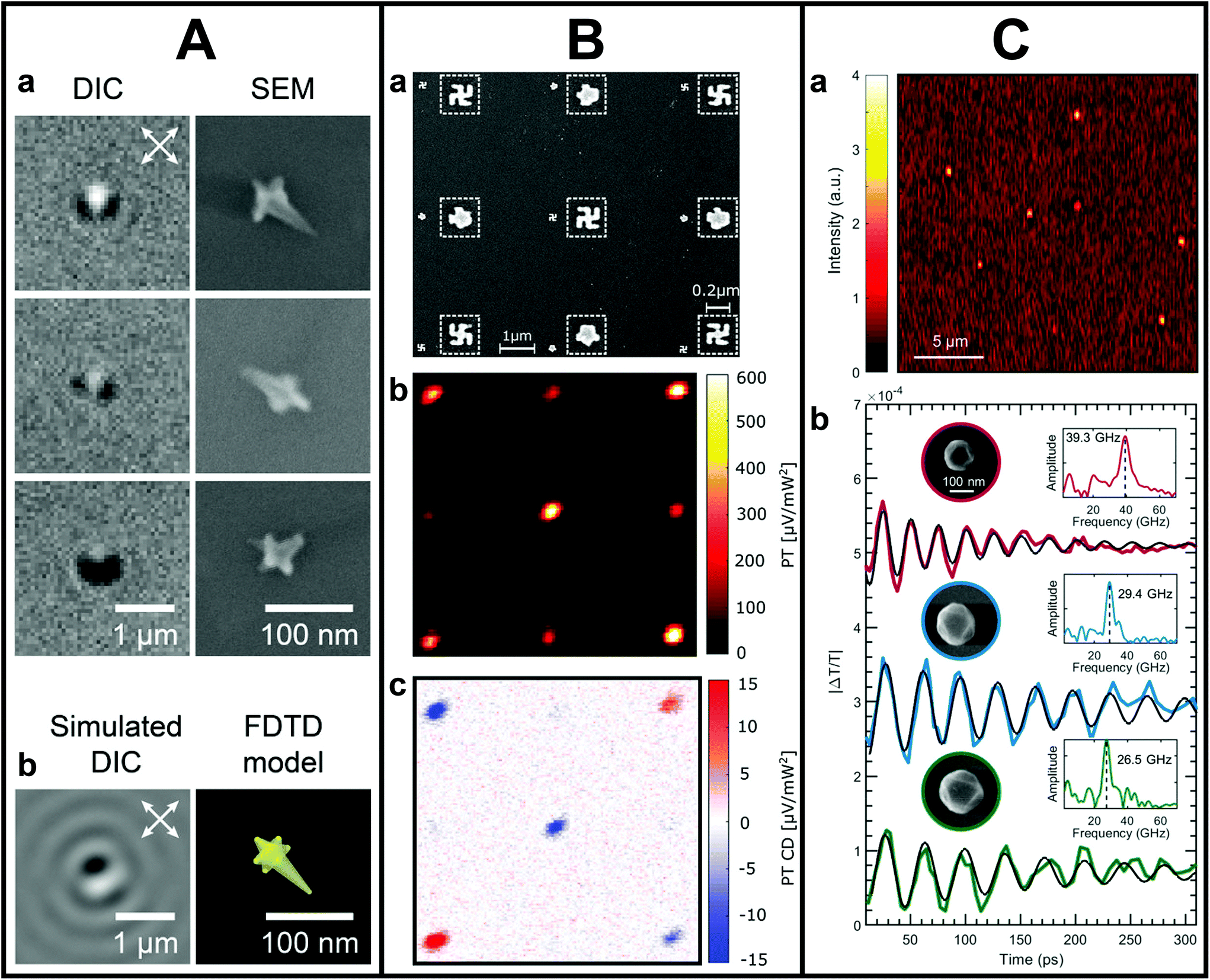 | ||
| Fig. 1 A. Orientation and symmetry characterization by differential interference contrast (DIC) and SEM. (a) Correlated SEM and DIC images of Au nanostars showing lobed DIC image patterns. (b) Simulated DIC images and 3D model of a Au nanostar. This figure has been adapted from ref. 78 with permission from the American Chemical Society, copyright 2018. B. Correlated SEM and photothermal CD measurements on nanogammadia. (a) SEM image of a 9 × 9 nanogammadia array with its corresponding photothermal image (b) and photothermal circular dichroism image (c). This figure has been adapted from ref. 82 with permission from the American Chemical Society, copyright 2019. C. Ultrafast pump–probe studies on single Al NSs correlated to SEM. (a) Representative transient extinction image of colloidal Al nanostructures used to locate individual particles. (b) Pump–probe ultrafast acoustic vibrations for single colloidal Al nanostructures with diameters of 125 (red), 161 (blue), and 181 nm (green). Data are offset for better comparison. This figure has been adapted from ref. 86 with permission from the American Chemical Society, copyright 2020. | ||
The exact knowledge of morphology is as important when dealing with NSs with complex geometries such as NS dimers. Hu et al. were among the first to study polarization dependent DFS and PL on single Au nanodisk dimers.72 The orientation and exact gap size of the dimers obtained by means of SEM allowed for a detailed interpretation of the observed optical features in terms of plasmonic coupling. However, the morphological correlation for such dimers through SEM might be limited by its spatial resolution. Su et al., for instance, showed the limits of the unambiguous interpretation of charge transfer plasmons in terms of their morphology of sub-nm spaced Au nanoblock dimers due to the lack of spatial resolution.79
Next to NS dimers, detailed single metal NS structure–property correlation is also important for chiral structures, which cause circular dichroism (CD), the differential absorption between left- and right-handed circularly polarized light.80,81 The polarization of light can be manipulated in various manners, which allows for measuring CD optically, nowadays even on a single NS level. For example, Spaeth et al. developed CD pump–probe photothermal microscopy with unprecedented sensitivity.82,83 To test the validity of the technique, the measured CD signals of chiral nanogammadia were correlated to their SEM morphology, demonstrating that through photothermal CD the strength and handedness of chiral nano-objects could be unambiguously determined (Fig. 1B).82 However, Karst et al. showed that morphology is insufficient to fully explain plasmonic chirality of solution-synthesized chiral NSs.84 From correlating SEM information and chiral scatterometry on a single NS level, the authors could not unambiguously identify geometric chiral features that led to specific spectral CD responses. These examples show that our understanding of nanoscale plasmonic chirality is not complete and that more detailed correlations of structural and optical features are needed at the individual NS level to explain these discrepancies.
One strength of using optics for accessing the metal NS properties is the possibility to simultaneously use different techniques in a multimodal way. In recent work, a combination of diverse techniques was used to simultaneously measure electromagnetic, catalytic and electronic processes by combining single-particle SERS with extinction measurements on nanocubes-on-a-mirror. In this manner, Oksenberg and co-workers mapped the plasmon-driven reactivity landscape of methylene blue.85 The correlation to SEM was crucial to ensure that only single nanoreactors were measured optically. In addition, by using optical techniques, the combination of ultrafast measurements with structural correlations becomes feasible as well on an individual NS level. For example, the recent correlation of single-particle femtosecond time-resolved pump–probe spectroscopy with SEM revealed the dependence of acoustic vibrations in Al nanostructures on size, shape and crystallinity (see Fig. 1C).86
2.2. Combination of single-particle optical spectroscopy and 2D/3D morphological characterization by (S)TEM on the same metal NS
The spatial resolution of SEM is insufficient when (sub-)nm or even atomic features need to be resolved. In cases where higher spatial resolution is needed or the 3D morphology needs to be known, the correlation to (S)TEM instead of SEM gives the necessary insight. Typical TEM grids are made of polymers and carbon and are therefore not always suitable as optical substrates. However, silicon nitride and silicon dioxide TEM grids are also commercially available, which facilitates such advanced correlation studies. The actual correlation can be done by pattern recognition87 or careful patterning of the substrates.88A detailed correlation between optical properties and sub-nm features of metal NSs,89,90 such as sub-nm gap size and NS morphology,91–97 can be achieved in this manner. This is particularly important for understanding charge transfer in metal NSs, either through direct contact or electron tunneling. For example, Zheng et al. combined single-particle PL and DFS with TEM to investigate the electron transfer at the interface between plasmonic Au nanorods and Pt cocatalysts.98 As revealed by TEM on the same individual NS, the location and distribution of Pt was hereby an important factor. Yang et al. correlated the gap distance down to sub-nm scales with plasmonic properties measured by DFS of gold NS dimers to investigate electron tunneling in the quantum regime, as shown in Fig. 2A.95 In their case, the resolution limit of their TEM complicated the unambiguous determination whether some dimers were in contact. In principle, however, state-of-the-art (S)TEMs can routinely reach atomic resolution, which makes the correlation with atomic-scale features and optical properties possible. More recently, in the work by Lerch and Reinhard,99 the charge transfer enhancement driven by the presence of interstitial palladium in Au NS dimers was investigated (see Fig. 2B). The influence of gap distance, density and location of Pd particles on the plasmon-driven charge transfer was explored by correlating TEM images of single dimers with their respective dark-field spectra. By doing this individual dimer correlation, the authors surprisingly found that even for dimer separations of more than 4 nm efficient electron transport could take place.
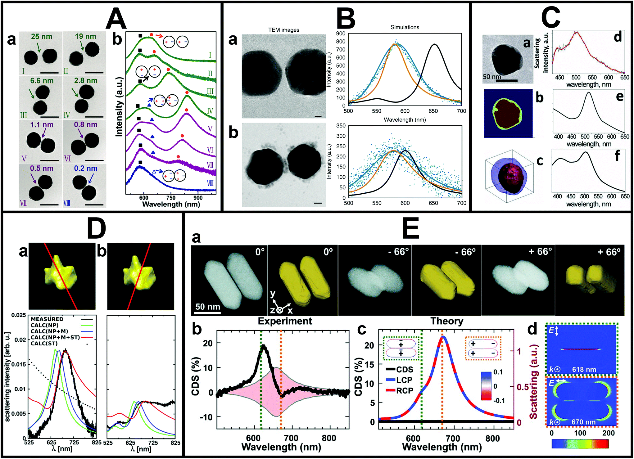 | ||
| Fig. 2 A. Correlated DFS-TEM measurements on Au NS dimers. (a) TEM images of Au NS dimers with an average diameter of 80 ± 2 nm. (b) Corresponding unpolarised dark-field scattering spectra of the same dimers. Black squares: transverse dipole mode, blue triangles: quadrupole plasmon mode, red circles: longitudinal bonding dipole, and hollow triangles: charge transfer mode. Scale bars are 100 nm. This figure has been adapted from ref. 95 with permission from the American Chemical Society, copyright 2016. B. Correlated scattering spectroscopy and TEM analysis of Au NS dimers with DNA (a) and also Pd (b) in the gap with spectra corresponding to experimental (blue), finite-difference time-domain (FDTD) simulated (black) and corrected FDTD (orange) spectra. Scale bars are 10 nm. This figure has been adapted from ref. 99 with permission from Springer Nature, copyright 2018. C. Correlation of electron tomography and DFS on single bimetallic NSs. (a) 2D TEM image of the Au core–Ag shell NS, (b) its core and shell assignment based on the 2D projection and (c) its electron tomography reconstruction corresponding (d) measured and (e, f) simulated spectra. This figure has been adapted from ref. 102 with permission from the American Chemical Society, copyright 2012. D. Correlated electron tomography and DFS measurements on a Au nanostar. Measured and simulated Rayleigh scattering spectra for two incident polarizations, (a) and (b), of a complex-shaped gold nanostar and the corresponding electron tomography reconstruction. This figure has been adapted from ref. 103 with permission from the American Chemical Society, copyright 2014. E. Chirality measurements of single Au NS–protein complexes correlated to TEM. (a) STEM tilt images and their electron tomography reconstruction of a Au nanorod dimer–BSA complex and its experimental single-particle circular differential scattering spectrum (b). (c) The corresponding simulated scattering spectra for incident left- and right-circularly polarized light. (d) Cross-sectional view of calculated near-field enhancement. This figure has been adapted from ref. 104 with permission from the American Association for the Advancement of Science, copyright 2019. | ||
In addition to high resolution capabilities, using TEM for structural correlation opens up a whole range of advanced TEM techniques. In particular, the combination with electron tomography has proven to be very powerful. Electron tomography allows one to reconstruct the 3D structure from a series of 2D images along different projection directions.100,101 By correlative measurements, Chuntonov and co-workers showed that the full 3D morphological information was actually needed to accurately reproduce the measured plasmon spectra of single Au core–Ag shell near-spherical NSs by simulations, see Fig. 2C.102 Perassi et al. also found an excellent agreement between the measured far-field optical properties and electromagnetic simulations when using the input knowledge from electron tomography (Fig. 2D).103 Furthermore, they showed that the orientation and location of contact points of the NS on the substrate need to be taken into account for the best match. The correlation to electron tomography has also been used to link structural chirality and plasmon-coupled CD. In the work by Zhang et al., single-particle circular differential scattering spectroscopy, STEM imaging at different tilt angles, and simulations were integrated to investigate the mechanisms behind CD enhancement of Au nanorods–bovine serum albumin complexes, as shown in Fig. 2E.104 Performing this correlation experiment at a single-particle level was necessary to distinguish between structural chirality and plasmon-coupled CD. Furthermore, it allowed to demonstrate the possibility of approaching single-molecule chirality sensing and hence the great potential of exploiting plasmon-coupled CD for biomolecules and biomarkers identification.81,105
Despite all the advantages of TEM, some bottlenecks need to be considered for using TEM in correlative studies. First of all, the samples need to be sufficiently thin to allow the electron beam to pass through, which makes the substrates fragile and difficult to handle. Furthermore, when the optical measurements are performed by immersing the grid in objective-matching liquids, these liquids need to be carefully removed to avoid subsequent contamination in the TEM. Secondly, electron beam damage is normally a larger problem in TEM compared to SEM due to the high energetic electrons.106–108 Especially in situ experiments are affected by electron-beam induced changes and one should be careful when comparing experimental results with theoretical calculations.107,109 For example, the interaction of the electron beam with the ligands on the metal NSs was proven to irreversibly modify their plasmon resonances as they get generally transformed into amorphous carbonaceous material.106,107 The consequent modest red-shift and broadening of the resonance peaks observed for individual metal NSs upon carbon contamination becomes dramatic for coupled asymmetric NS dimers, which consequently exhibited Fano resonances.106 Using a lower energy electron beam and reducing the presence of contaminants, by for instance plasma cleaning,109 can be explored as ways to reduce this effect. However, it was shown that the current methods used to remove the surface ligands are still not fully satisfactory.109 Where possible we therefore recommend to do any optical property characterization before exposing the sample to the electron beam. In this regard, atomic force microscopy (beyond the scope of this Minireview) is an alternative to EM to investigate morphology of electron-beam sensitive samples when there are no strong constraints on spatial resolution. In addition, optical near-field techniques, which can surpass the traditional diffraction limit of light, are an attractive alternative as well and we would like to guide the reader to specialized reviews.35,110–113
2.3. Single metal NS light-induced structural modifications monitored by EM
The combination of EM and light is not only relevant for structure–property correlation purposes, as shown so far, but also to investigate light-induced changes of individual metal NSs by directly comparing the morphology before and after laser excitation. Performing such studies on an individual NS level gives us more insight in the underlying physics of below melting threshold reshaping and possibly allows for dynamical tracking of the process. In this manner, it becomes feasible to control the reshaping process and create tailored out-of-equilibrium nanostructures. Moreover, light-induced changes can also be used as a tool to iteratively connect minute morphology changes to property modifications on the same NS.114 Zijlstra et al. reported one of the first studies that elucidated the underlying physics of photothermal reshaping of Au nanorods.55 By correlating white light scattering spectroscopy and SEM before and after laser-induced reshaping, the authors quantified the melting energy of a single Au nanorod and observed that nanorods with longer aspect ratios were thermodynamically less stable than shorter ones. Another remarkable reshaping study was conducted by Wang and Ding, in which they combined the photothermal effect and optical forces of the laser beam to stretch and eventually break spherical Au NSs into dimers (Fig. 3A).115 Next to visualizing the reshaped NSs, the authors also determined their scattering properties and used that to follow the reshaping dynamics.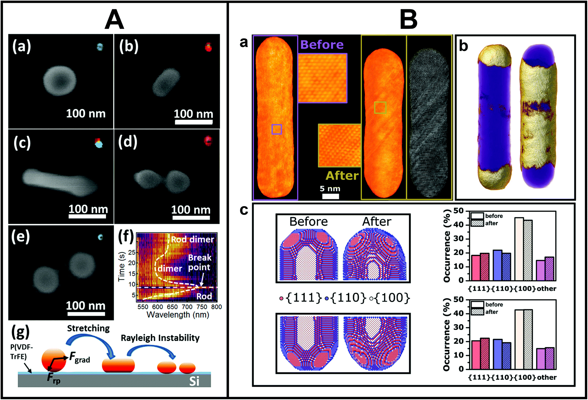 | ||
| Fig. 3 A. Morphological changes upon photothermal reshaping of Au NSs tracked by SEM. (a–e) SEM images of a Au NS irradiated (2 mW) for different periods of time: (a) 0 s (b) 3 s, (c) 5 s, (d) 8 s, (e) 20 s. Insets are dark-field scattering images of the Au NS after irradiation. (f) Scattering spectra evolution during the deformation process. (g) Scheme of the proposed photothermal deformation mechanism. This figure has been reproduced from ref. 115 with permission from the American Chemical Society, copyright 2019. B. Atomic-scale modifications of the same mesoporous silica-coated Au nanorod after femtosecond laser reshaping. (a) 3D reconstruction of the same Au nanorod before (left) and after (right) femtosecond laser excitation. Whereas the nanorod was defect-free before irradiation, clear atomic lattice defects occurred after irradiation (insets). (b) Redistributed volume upon laser excitation. The left and right side indicate local volume increases and decreases (gold), respectively, overlaid on the overall nanorod morphology (purple). (c) Quantitative facet distribution before and after laser excitation. This figure has been adapted from ref. 116 with permission from Wiley, copyright 2021. | ||
With the correlation to TEM, the understanding of the underlying mechanism could be additionally enhanced. Taylor and co-workers correlated the aspect ratio and orientation of the same individual Au nanorods before and after femtosecond laser irradiation by TEM, which allowed them to extract a quantitative surface-driven diffusion model of the underlying reshaping mechanism.57 A few years later, Albrecht et al. demonstrated by single-particle correlation that a mesoporous surface coating around Au nanorods enhanced their photothermal stability and that intermediate reshaping morphologies differed from uncoated nanorods.58 The authors recently extended their work to the atomic scale by performing atomically-resolved electron tomography before and after laser-induced reshaping on the same NS,116 as shown in Fig. 3B. The 3D atomic-scale information served as an input for molecular dynamics simulations, which allowed to unravel the complicated atomistic processes underlying the ultrafast reshaping and demonstrated that atomic imperfections significantly influenced these processes. This detailed knowledge will potentially make it possible to tune the morphology as well as atomic structure of metal NSs, an important prerequisite for enhanced catalytic applications.
3. In situ light-driven single metal NS property correlation and morphology modification inside the TEM
The single metal NS light-electron microscopy correlation studies highlighted so far were performed ex situ, meaning that the optical and structural characterizations were carried out completely independently. However, it should be kept in mind that metal NSs can restructure in different environments,117 resulting in possible discrepancies between the optical measurements performed in ambient conditions and morphology measured by EM in vacuum. To simultaneously assess physical (optical, electronic and catalytic) and sub-nm morphological properties of the same plasmonic NSs, in situ experiments under light excitation inside the electron microscope are needed. The community has particularly focused on such in situ studies inside the TEM owing to the high spatial resolution. However, the limited space between the objective lens pole pieces, where the sample is located, as well as the high vacuum of the TEM column adds to the challenges of introducing light excitation inside the TEM. There are essentially two ways. On the one hand, light can be introduced via a holder, either the sample holder itself or a retractable additional holder.118 In both cases, the holder needs to fit in the narrow space between the pole pieces. A smart light-incoupling holder design can even enable ultrafast optical studies in situ in a TEM with atomic resolution.119 On the other hand, light can be introduced into the TEM column and directed towards the specimen via a mirror above the pole pieces. In the latter case, the column needs to be modified but the space between the pole pieces stays available for additional in situ holders (e.g. heating, gas, liquid or electric biasing) or electron tomography.120–123In this manner, first in situ and in operando studies of metal NSs under light excitation were demonstrated. Such studies are not only critical to perform detailed in situ structure–property characterization, but also to follow light-mediated catalytic processes118,124,125 and morphological changes induced by laser excitation.62,120,126 For example, Dionne and co-workers directly coupled optical sources and detectors into an environmental TEM.118,124,125 This optically coupled-electron microscope was used by Vadai et al. to monitor single-particle photocatalysis (Fig. 4A).124 Dynamic phase transformations of plasmon-induced photocatalytic reactions with sub-2 nm spatial resolution were measured through STEM contrast imaging. Performing this experiment on a single-particle level allowed to statistically show that the active sites, where the catalytic reactions took place preferentially, corresponded to the plasmonic hotspots. Matsumura and co-workers introduced light from a nanosecond pulsed laser directly into a high-voltage TEM.126 This set-up allowed to reveal the evolution of the atomic reorganization of Au nanorods one laser pulse at a time (Fig. 4B). Voss et al. unravelled that Coulomb fission was behind the laser-induced reshaping of spherical plasmonic NSs and captured its complex dynamics, as shown in Fig. 4C.120
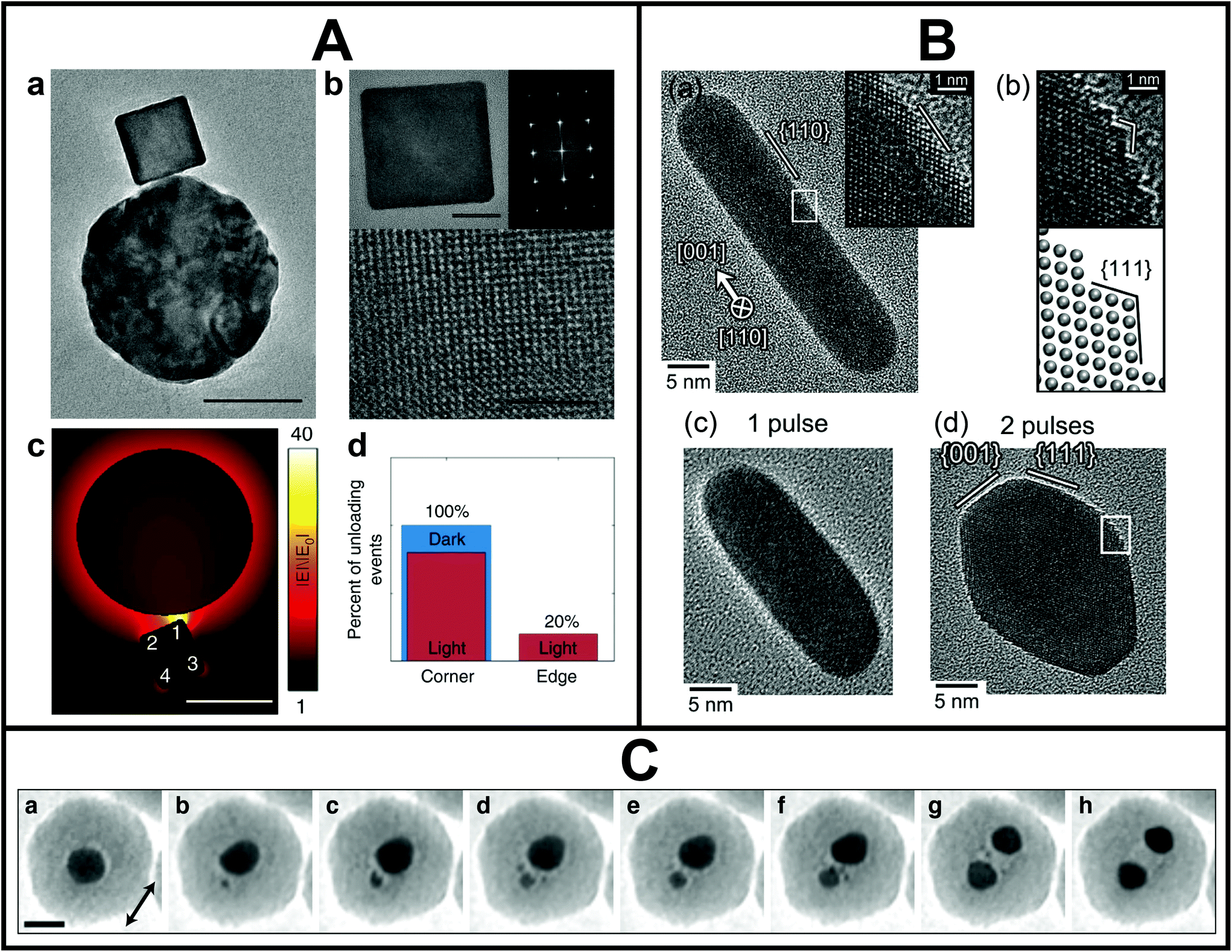 | ||
| Fig. 4 A. Plasmon-controlled photocatalytic reaction measured inside the TEM. (a) TEM and (b) high-resolution TEM images of an antenna (Au)–reactor (Pd) system. (c) Calculated near-field enhancement for the antenna (Au)–reactor (Pd) system under illumination. (d) Extracted percentage of hydrogen desorption from corner and edge sites with (red) and without (blue) illumination. Data were obtained through in situ STEM movies of the phase transformation reaction in a single antenna-reactor. Scale bars are 50 nm (a and c) and 10 and 2 nm, respectively (b). This figure has been adapted from ref. 124 with permission from Springer Nature, copyright 2018. B. High-resolution TEM images of a nanorod under nanosecond pulsed laser irradiation at an average pulse intensity of 980 J m−2: before irradiation (a), after irradiation with one pulse (c) and after irradiation with two pulses (d). (b) Magnified image of inset in (d) with schematic lattice drawing. This figure has been adapted from ref. 126 with permission from Oxford University Press, copyright 2019. C. In situ observation of coulombic fission of gold NSs encapsulated in a silica shell under intense femtosecond laser irradiation. Scale bar is 20 nm. This figure has been adapted from ref. 120 with permission from the American Chemical Society, copyright 2019. | ||
In recent years, light incoupling has also been combined with ultrafast temporal resolution by either newly developed ultrafast electron beam blankers or by generating ultrashort electron pulses through laser illumination of the electron gun.121,127–131 Together with the development of novel electron detectors, this approach opened up a number of impressive time-resolved pioneering studies.122 For example, in recent work by Olshin et al. high spatial resolution imaging with single-shot microsecond temporal resolution was obtained by using an electrostatic deflector to chop the electron beam from a continuous source into short packets.129 The combination with light excitation of the sample inside the TEM allowed the authors to investigate the mechanisms behind light-induced crystallization and amorphization of individual metal NSs. Such experiments are extremely promising as they bring the ultimate combination of structural, morphological, chemical and optical characterization on single NSs with ultrafast temporal resolution into the realm of what is achievable. It needs to be kept in mind, however, that the electron beam effects are more significant in the discussed in situ approach, which might therefore not be suitable for samples prone to electron beam damage.
4. Conclusion and outlook
In this Minireview we presented example studies from recent years in which the direct structure–property correlation or light induced morphological changes were investigated by coupling light and EM on the same single metal NS, either in a consecutive ex situ manner or in situ inside the electron microscope. Taking individual metal NSs as a case study, we demonstrated that these detailed correlations brought new insights into physics and materials science of plasmonic nanosystems. Gaining access to the full dynamic and structural changes with simultaneous ultrafast temporal resolution and atomic scale spatial resolution is the ultimate dream.132 As touched upon in the previous section, in the last few years EM groups have worked hard to overcome the poor temporal resolution in EM and several advances in ultrafast EM have been demonstrated with either novel fast electron detectors or modified electron sources.121,127–131 Ultimately, it might even become possible to integrate additional analytic tools into UTEMs (e.g. Raman spectroscopy, mass spectrometry, and ultrasensitive gas-phase molecular spectroscopy) to truly follow dynamic processes such as plasmonic-enhanced chemical reactions with very high spatial resolution. The development of faster EM techniques becomes even more important for electron tomography, where the acquisition can take up to 1 hour. Recent approaches to fast electron tomography101 open the pathway to combine 3D information with in operando studies.Next to the limited time resolution in EM, another bottleneck of the discussed single metal NS correlative approaches is the rather low characterization throughput due to the involvement of EM. This limitation is for example evident in the previously cited work by Oksenberg et al.,85 where statistics over a thousand individual nanoreactors was needed to extract meaningful results. This drawback can be addressed by automating correlative workflows or at least the EM experiments, possibly through the help of machine learning.133 Such automation would dramatically improve the speed of acquisitions and therefore the statistics, allowing for imaging of more particles and larger sample volumes in shorter time. In life sciences, such automated workflow systems are already state-of-the-art,134 whereas they have not yet found a widespread adoption in material science. Finally, inferring structural information directly from the optical spectra can be investigated as another strategy to overcome the limitations of electron beam damage, temporal resolution and statistics arising from the need of EM to correlate morphology to optical properties of NSs.78,135–138 For example, Payne et al. used high throughput quantitative extinction microscopy in combination with electromagnetic simulations to measure the size and shape of metal NSs fully optically.135 Dawson and co-workers demonstrated that it is also possible to detect the shape of anisotropic gold NSs in dispersion by optical means.138 Shiratori et al. used machine learning to determine the size and aspect ratio of Au nanorods from scattering spectra.136 Although the possibility to extend the proposed approaches to more complex structures still needs to be further investigated, theoretically this idea seems very promising. Ideally, this could be extended to a quantified classification in which NSs with different geometries and sizes can be compared based on their nanoscale-shape, which has also been deemed essential in their interaction with living matter.139,140
Ultimately, the choice of the correlative approach depends on the experiment and the research question that needs to be answered. Here, we highlighted the importance of combining optical characterization and/or light interaction with information on sub-nm morphological properties at the single metal NS level. This single-particle correlation performed on the exact same individual metal NS is not only critical at a fundamental level, but also to optimize performances of metal NSs in practical applications, such as light management, sensing, biomedicine and catalysis. As laid out above, we believe that further developments in in situ integration of EM and optical characterization, limiting the damage of the electron beam, improving spatial and temporal resolution, developing automated workflows and manipulating NSs using light will provide more detailed insights on the structure–property relationship in promising nanomaterials, leading to the growth of this field in the near future.
Author contributions
W. A. initiated the project. M. D. and F. S. performed an extensive literature study under the supervision of W. A. All authors co-wrote the manuscript.Conflicts of interest
There are no conflicts to declare.Acknowledgements
This work is part of the research program of AMOLF, which is partly financed by the Dutch Research Council (NWO). We thank Eitan Oksenberg for critically reading the manuscript and for the useful comments and suggestions.References
- K. L. Kelly, E. Coronado, L. L. Zhao and G. C. Schatz, J. Phys. Chem. B, 2003, 107, 668–677 CrossRef CAS.
- C. J. Orendorff, T. K. Sau and C. J. Murphy, Small, 2006, 2, 636–639 CrossRef CAS PubMed.
- J. J. Mock, M. Barbic, D. R. Smith, D. A. Schultz and S. Schultz, J. Chem. Phys., 2002, 116, 6755–6759 CrossRef CAS.
- B. J. Wiley, S. H. Im, Z.-Y. Li, J. McLellan, A. Siekkinen and Y. Xia, J. Phys. Chem. B, 2006, 110, 15666–15675 CrossRef CAS PubMed.
- E. Ringe, M. R. Langille, K. Sohn, J. Zhang, J. Huang, C. A. Mirkin, R. P. V. Duyne and L. D. Marks, J. Phys. Chem. Lett., 2012, 3, 1479–1483 CrossRef CAS PubMed.
- K. B. Mogensen and K. Kneipp, J. Phys. Chem. C, 2014, 118, 28075–28083 CrossRef CAS.
- S. Link, Z. L. Wang and M. A. El-Sayed, J. Phys. Chem. B, 1999, 103, 3529–3533 CrossRef CAS.
- S. D. Lounis, E. L. Runnerstrom, A. Bergerud, D. Nordlund and D. J. Milliron, J. Am. Chem. Soc., 2014, 136, 7110–7116 CrossRef CAS PubMed.
- T. M. de Oliveira, W. Albrecht, G. González-Rubio, T. Altantzis, I. P. L. Hoyos, A. Béché, S. V. Aert, A. Guerrero-Martínez, L. M. Liz-Marzán and S. Bals, ACS Nano, 2020, 14, 12558–12570 CrossRef PubMed.
- L. Wang, M. H. Kafshgari and M. Meunier, Adv. Funct. Mater., 2020, 30, 2005400 CrossRef CAS.
- D. Astruc, Chem. Rev., 2020, 120, 461–463 CrossRef CAS PubMed.
- H. T. Phan and A. J. Haes, J. Phys. Chem. C, 2019, 123, 16495–16507 CrossRef CAS PubMed.
- H. Kang, J. T. Buchman, R. S. Rodriguez, H. L. Ring, J. He, K. C. Bantz and C. L. Haynes, Chem. Rev., 2019, 119, 664–699 CrossRef CAS PubMed.
- L. Cavigli, B. N. Khlebtsov, S. Centi, N. G. Khlebtsov, R. Pini and F. Ratto, Nanomaterials, 2021, 11, 116 CrossRef CAS PubMed.
- L. M. Liz-Marzan, Colloidal Synthesis of Plasmonic Nanometals, Jenny Stanford Publishing, 1st edn, 2021 Search PubMed.
- G. Gonzalez-Rubio, J. Mosquera, V. Kumar, A. Pedrazo-Tardajos, P. Llombart, D. M. Solis, I. Lobato, E. G. Noya, A. Guerrero-Martinez, J. M. Taboada, F. Obelleiro, L. G. MacDowell, S. Bals and L. M. Liz-Marzan, Science, 2020, 368, 1472–1477 CrossRef CAS PubMed.
- K. D. Gilroy, A. Ruditskiy, H.-C. Peng, D. Qin and Y. Xia, Chem. Rev., 2016, 116, 10414–10472 CrossRef CAS PubMed.
- C. J. Murphy, T. K. Sau, A. M. Gole, C. J. Orendorff, J. Gao, L. Gou, S. E. Hunyadi and T. Li, J. Phys. Chem. B, 2005, 109, 13857–13870 CrossRef CAS PubMed.
- S. L. A. Bueno, J. T. L. Gamler and S. E. Skrabalak, ChemNanoMat, 2020, 6, 783–789 CrossRef CAS.
- H.-E. Lee, H.-Y. Ahn, J. Mun, Y. Y. Lee, M. Kim, N. H. Cho, K. Chang, W. S. Kim, J. Rho and K. T. Nam, Nature, 2018, 556, 360–365 CrossRef CAS PubMed.
- S. E. Skrabalak, Acc. Mater. Res., 2021, 2, 621–629 CrossRef CAS.
- Z.-P. Wu, S. Shan, S.-Q. Zang and C.-J. Zhong, Acc. Chem. Res., 2020, 53, 2913–2924 CrossRef CAS PubMed.
- S. M. E. Peters, M. A. Verheijen, M. W. J. Prins and P. Zijlstra, Nanotechnology, 2016, 27, 024001 CrossRef CAS PubMed.
- M. Hu, C. Novo, A. Funston, H. Wang, H. Staleva, S. Zou, P. Mulvaney, Y. Xia and G. V. Hartland, J. Mater. Chem., 2008, 18, 1949 RSC.
- C. Sönnichsen, T. Franzl, T. Wilk, G. von Plessen, J. Feldmann, O. Wilson and P. Mulvaney, Phys. Rev. Lett., 2002, 88, 077402 CrossRef PubMed.
- E. Ringe, B. Sharma, A.-I. Henry, L. D. Marks and R. P. Van Duyne, Phys. Chem. Chem. Phys., 2013, 15, 4110 RSC.
- A.-I. Henry, J. M. Bingham, E. Ringe, L. D. Marks, G. C. Schatz and R. P. V. Duyne, J. Phys. Chem. C, 2011, 115, 9291–9305 CrossRef CAS.
- P. Zijlstra and M. Orrit, Rep. Prog. Phys., 2011, 74, 106401 CrossRef.
- L. Tong, H. Wei, S. Zhang, Z. Li and H. Xu, Phys. Chem. Chem. Phys., 2013, 15, 4100 RSC.
- J. B. Sambur and P. Chen, Annu. Rev. Phys. Chem., 2014, 65, 395–422 CrossRef CAS PubMed.
- J. Olson, S. Dominguez-Medina, A. Hoggard, L.-Y. Wang, W.-S. Chang and S. Link, Chem. Soc. Rev., 2015, 44, 40–57 RSC.
- B. S. Hoener, S. R. Kirchner, T. S. Heiderscheit, S. S. Collins, W.-S. Chang, S. Link and C. F. Landes, Chem, 2018, 4, 1560–1585 CAS.
- S. Alekseeva, I. I. Nedrygailov and C. Langhammer, ACS Photonics, 2019, 6, 1319–1330 CrossRef CAS.
- J. Zhou, A. I. Chizhik, S. Chu and D. Jin, Nature, 2020, 579, 41–50 CrossRef CAS PubMed.
- A. Al-Zubeidi, L. A. McCarthy, A. Rafiei-Miandashti, T. S. Heiderscheit and S. Link, Nanophotonics, 2021, 10, 1621–1655 CrossRef CAS.
- J. Boken, P. Khurana, S. Thatai, D. Kumar and S. Prasad, Appl. Spectrosc. Rev., 2017, 52, 774–820 CrossRef CAS.
- G. Park, K. S. Min, H. Kwon, S. Yoon, S. Park, J. Kwon, S. Lee, J. Jo, M. Kim and S. K. Kim, Adv. Mater., 2021, 33, 2100653 CrossRef CAS PubMed.
- X. Wang, C. Liu, C. Gao, K. Yao, S. S. M. Masouleh, R. Berté, H. Ren, L. de S. Menezes, E. Cortés, I. C. Bicket, H. Wang, N. Li, Z. Zhang, M. Li, W. Xie, Y. Yu, Y. Fang, S. Zhang, H. Xu, A. Vomiero, Y. Liu, G. A. Botton, S. A. Maier and H. Liang, ACS Nano, 2021, 15, 10553–10564 CrossRef PubMed.
- J. A. Scholl, A. García-Etxarri, A. L. Koh and J. A. Dionne, Nano Lett., 2013, 13, 564–569 CrossRef CAS PubMed.
- G. Li, C. Cherqui, N. W. Bigelow, G. Duscher, P. J. Straney, J. E. Millstone, D. J. Masiello and J. P. Camden, Nano Lett., 2015, 15, 3465–3471 CrossRef CAS PubMed.
- J. Lee, D. Jeon and J. Yeo, Adv. Mater., 2021, 33, 2006606 CrossRef CAS PubMed.
- M. Kociak and O. Stéphan, Chem. Soc. Rev., 2014, 43, 3865 RSC.
- A. C. Atre, B. J. M. Brenny, T. Coenen, A. García-Etxarri, A. Polman and J. A. Dionne, Nat. Nanotechnol., 2015, 10, 429–436 CrossRef CAS PubMed.
- T. Coenen, B. J. Brenny, E. J. Vesseur and A. Polman, MRS Bull., 2015, 40, 359–365 CrossRef CAS.
- C. Colliex, M. Kociak and O. Stéphan, Ultramicroscopy, 2016, 162, A1–A24 CrossRef CAS PubMed.
- A. Polman, M. Kociak and F. J. G. de Abajo, Nat. Mater., 2019, 18, 1158–1171 CrossRef CAS PubMed.
- F. J. G. de Abajo and V. D. Giulio, ACS Photonics, 2021, 8, 945–974 CrossRef PubMed.
- L. Slaughter, W.-S. Chang and S. Link, J. Phys. Chem. Lett., 2011, 2, 2015–2023 CrossRef CAS.
- G. V. Hartland, Chem. Rev., 2011, 111, 3858–3887 CrossRef CAS PubMed.
- A. Joplin, W.-S. Chang and S. Link, Langmuir, 2018, 34, 3775–3786 CrossRef CAS PubMed.
- R. F. Hamans, R. Kamarudheen and A. Baldi, Nanomaterials, 2020, 10, 2377 CrossRef CAS PubMed.
- T. Jollans, M. D. Baaske and M. Orrit, J. Phys. Chem. C, 2019, 123, 14107–14117 CrossRef CAS.
- P. F. Gao, G. Lei and C. Z. Huang, Anal. Chem., 2021, 93, 4707–4726 CrossRef CAS PubMed.
- S. Adhikari, P. Spaeth, A. Kar, M. D. Baaske, S. Khatua and M. Orrit, ACS Nano, 2020, 14, 16414–16445 CrossRef CAS PubMed.
- P. Zijlstra, J. W. M. Chon and M. Gu, Phys. Chem. Chem. Phys., 2009, 11, 5915 RSC.
- G. González-Rubio, A. Guerrero-Martínez and L. M. Liz-Marzán, Acc. Chem. Res., 2016, 49, 678–686 CrossRef PubMed.
- A. B. Taylor, A. M. Siddiquee and J. W. M. Chon, ACS Nano, 2014, 8, 12071–12079 CrossRef CAS PubMed.
- W. Albrecht, T.-S. Deng, B. Goris, M. A. van Huis, S. Bals and A. van Blaaderen, Nano Lett., 2016, 16, 1818–1825 CrossRef CAS PubMed.
- S. Link, C. Burda, B. Nikoobakht and M. A. El-Sayed, J. Phys. Chem. B, 2000, 104, 6152–6163 CrossRef CAS.
- A. R. Ziefuss, S. Reich, S. Reichenberger, M. Levantino and A. Plech, Phys. Chem. Chem. Phys., 2020, 22, 4993–5001 RSC.
- L. Delfour and T. E. Itina, J. Phys. Chem. C, 2015, 119, 13893–13900 CrossRef CAS.
- G. Bongiovanni, P. K. Olshin, C. Yan, J. M. Voss, M. Drabbels and U. J. Lorenz, Nanoscale Adv., 2021, 3, 5277–5283 RSC.
- G. González-Rubio, T. M. de Oliveira, W. Albrecht, P. Díaz-Núñez, J. C. Castro-Palacio, A. Prada, R. I. González, L. Scarabelli, L. Bañares, A. Rivera, L. M. Liz-Marzán, O. Peña-Rodríguez, S. Bals and A. Guerrero-Martínez, J. Phys. Chem. Lett., 2020, 11, 670–677 CrossRef PubMed.
- G. González-Rubio, P. Díaz-Núñez, W. Albrecht, V. Manzaneda-González, L. Bañares, A. Rivera, L. M. Liz-Marzán, O. Peña-Rodríguez, S. Bals and A. Guerrero-Martínez, Adv. Opt. Mater., 2021, 9, 2002134 CrossRef.
- Y. Lin, M. Zhou, X. Tai, H. Li, X. Han and J. Yu, Matter, 2021, 4, 2309–2339 CrossRef CAS.
- J. Rodríguez-Fernández, C. Novo, V. Myroshnychenko, A. M. Funston, A. Sánchez-Iglesias, I. Pastoriza-Santos, J. Pérez-Juste, F. J. G. de Abajo, L. M. Liz-Marzán and P. Mulvaney, J. Phys. Chem. C, 2009, 113, 18623–18631 CrossRef.
- L. S. Slaughter, W.-S. Chang, P. Swanglap, A. Tcherniak, B. P. Khanal, E. R. Zubarev and S. Link, J. Phys. Chem. C, 2010, 114, 4934–4938 CrossRef CAS.
- B. D. Clark, C. R. Jacobson, M. Lou, D. Renard, G. Wu, L. Bursi, A. S. Ali, D. F. Swearer, A.-L. Tsai, P. Nordlander and N. J. Halas, ACS Nano, 2019, 13, 9682–9691 CrossRef CAS PubMed.
- J. Asselin, C. Boukouvala, E. R. Hopper, Q. M. Ramasse, J. S. Biggins and E. Ringe, ACS Nano, 2020, 14, 5968–5980 CrossRef CAS PubMed.
- S. W. Moon and J. W. Ha, Phys. Chem. Chem. Phys., 2019, 21, 7061–7066 RSC.
- S. S. E. Collins, E. K. Searles, L. J. Tauzin, M. Lou, L. Bursi, Y. Liu, J. Song, C. Flatebo, R. Baiyasi, Y.-Y. Cai, B. Foerster, T. Lian, P. Nordlander, S. Link and C. F. Landes, ACS Nano, 2021, 15, 9522–9530 CrossRef PubMed.
- H. Hu, H. Duan, J. K. W. Yang and Z. X. Shen, ACS Nano, 2012, 6, 10147–10155 CrossRef CAS PubMed.
- Y. Fang, W.-S. Chang, B. Willingham, P. Swanglap, S. Dominguez-Medina and S. Link, ACS Nano, 2012, 6, 7177–7184 CrossRef CAS PubMed.
- Y.-Y. Cai, J. G. Liu, L. J. Tauzin, D. Huang, E. Sung, H. Zhang, A. Joplin, W.-S. Chang, P. Nordlander and S. Link, ACS Nano, 2018, 12, 976–985 CrossRef CAS PubMed.
- L. J. Tauzin, Y. yu Cai, K. W. Smith, S. A. H. Jebeli, U. Bhattacharjee, W.-S. Chang and S. Link, ACS Photonics, 2018, 5, 3541–3549 CrossRef CAS.
- B. Ostovar, Y.-Y. Cai, L. J. Tauzin, S. A. Lee, A. Ahmadivand, R. Zhang, P. Nordlander and S. Link, ACS Nano, 2020, 14, 15757–15765 CrossRef PubMed.
- T. Zhang, G. Lu, H. Shen, K. Shi, Y. Jiang, D. Xu and Q. Gong, Sci. Rep., 2015, 4, 3867 CrossRef PubMed.
- K. S. B. Culver, T. Liu, A. J. Hryn, N. Fang and T. W. Odom, J. Phys. Chem. Lett., 2018, 9, 2886–2892 CrossRef CAS PubMed.
- M.-N. Su, Q. Sun, K. Ueno, W.-S. Chang, H. Misawa and S. Link, J. Phys. Chem. C, 2018, 122, 18005–18011 CrossRef CAS.
- N. A. Kotov, L. M. Liz-Marzán and P. S. Weiss, ACS Nano, 2021, 15, 12457–12460 CrossRef CAS.
- L. A. Warning, A. R. Miandashti, L. A. McCarthy, Q. Zhang, C. F. Landes and S. Link, ACS Nano, 2021, 15, 15538–15566 CrossRef CAS PubMed.
- P. Spaeth, S. Adhikari, L. Le, T. Jollans, S. Pud, W. Albrecht, T. Bauer, M. Caldarola, L. Kuipers and M. Orrit, Nano Lett., 2019, 19, 8934–8940 CrossRef CAS PubMed.
- P. Spaeth, S. Adhikari, M. D. Baaske, S. Pud, J. Ton and M. Orrit, ACS Nano, 2021, 15, 16277–16285 CrossRef CAS PubMed.
- J. Karst, N. H. Cho, H. Kim, H.-E. Lee, K. T. Nam, H. Giessen and M. Hentschel, ACS Nano, 2019, 13, 8659–8668 CrossRef CAS PubMed.
- E. Oksenberg, I. Shlesinger, A. Xomalis, A. Baldi, J. J. Baumberg, A. F. Koenderink and E. C. Garnett, Nat. Nanotechnol., 2021, 16, 1378–1385 CrossRef CAS PubMed.
- B. Ostovar, M.-N. Su, D. Renard, B. D. Clark, P. D. Dongare, C. Dutta, N. Gross, J. E. Sader, C. F. Landes, W.-S. Chang, N. J. Halas and S. Link, J. Phys. Chem. A, 2020, 124, 3924–3934 CrossRef CAS PubMed.
- Y. Wang, S. Eswaramoorthy, L. Sherry, J. Dieringer, J. Camden, G. Schatz, R. Van Duyne and L. Marks, Ultramicroscopy, 2009, 109, 1110–1113 CrossRef CAS PubMed.
- R. Jin, J. E. Jureller and N. F. Scherer, Appl. Phys. Lett., 2006, 88, 263111 CrossRef.
- Y. Yang, C. Gu and J. Li, Small, 2019, 15, 1804177 CrossRef PubMed.
- H. Shi, X. Zhu, S. Zhang, G. Wen, M. Zheng and H. Duan, Nanoscale Adv., 2021, 3, 4349–4369 RSC.
- J. P. Camden, J. A. Dieringer, Y. Wang, D. J. Masiello, L. D. Marks, G. C. Schatz and R. P. Van Duyne, J. Am. Chem. Soc., 2008, 130, 12616–12617 CrossRef CAS PubMed.
- T.-S. Deng, J. Parker, Y. Yifat, N. Shepherd and N. F. Scherer, J. Phys. Chem. C, 2018, 122, 27662–27672 CrossRef CAS.
- J. H. Yoon, F. Selbach, L. Langolf and S. Schlücker, Small, 2018, 14, 1702754 CrossRef PubMed.
- L. Tian, C. Wang, H. Zhao, F. Sun, H. Dong, K. Feng, P. Wang, G. He and G. Li, J. Am. Chem. Soc., 2021, 143, 8631–8638 CrossRef CAS PubMed.
- L. Yang, H. Wang, Y. Fang and Z. Li, ACS Nano, 2016, 10, 1580–1588 CrossRef CAS PubMed.
- E. A. Sprague-Klein, R. Ho-Wu, D. Nguyen, S. C. Coste, Y. Wu, J. J. McMahon, T. Seideman, G. C. Schatz and R. P. V. Duyne, J. Phys. Chem. C, 2021, 125, 22142–22153 CrossRef CAS.
- P. S. Popp, J. F. Herrmann, E.-C. Fritz, B. J. Ravoo and C. Höppener, Small, 2016, 12, 1667–1675 CrossRef CAS PubMed.
- Z. Zheng, T. Tachikawa and T. Majima, J. Am. Chem. Soc., 2014, 136, 6870–6873 CrossRef CAS PubMed.
- S. Lerch and B. M. Reinhard, Nat. Commun., 2018, 9, 1608 CrossRef PubMed.
- P. A. Midgley and R. E. Dunin-Borkowski, Nat. Mater., 2009, 8, 271–280 CrossRef CAS PubMed.
- W. Albrecht and S. Bals, J. Phys. Chem. C, 2020, 124, 27276–27286 CrossRef CAS.
- L. Chuntonov, M. Bar-Sadan, L. Houben and G. Haran, Nano Lett., 2012, 12, 145–150 CrossRef CAS PubMed.
- E. M. Perassi, C. Hrelescu, A. Wisnet, M. Döblinger, C. Scheu, F. Jäckel, E. A. Coronado and J. Feldmann, ACS Nano, 2014, 8, 4395–4402 CrossRef CAS PubMed.
- Q. Zhang, T. Hernandez, K. W. Smith, S. A. H. Jebeli, A. X. Dai, L. Warning, R. Baiyasi, L. A. McCarthy, H. Guo, D.-H. Chen, J. A. Dionne, C. F. Landes and S. Link, Science, 2019, 365, 1475–1478 CrossRef CAS PubMed.
- K. Martens, F. Binkowski, L. Nguyen, L. Hu, A. O. Govorov, S. Burger and T. Liedl, Nat. Commun., 2021, 12, 2025 CrossRef CAS PubMed.
- H. Leng, B. Szychowski, M.-C. Daniel and M. Pelton, J. Phys. Chem. Lett., 2017, 8, 3607–3612 CrossRef CAS PubMed.
- W. Albrecht, A. van de Glind, H. Yoshida, Y. Isozaki, A. Imhof, A. van Blaaderen, P. E. de Jongh, K. P. de Jong, J. Zečević and S. Takeda, Ultramicroscopy, 2018, 193, 97–103 CrossRef CAS PubMed.
- R. Egerton, Micron, 2019, 119, 72–87 CrossRef CAS PubMed.
- R. D. Meyer, W. Albrecht and S. Bals, Micron, 2021, 144, 103036 CrossRef PubMed.
- N. Mauser and A. Hartschuh, Chem. Soc. Rev., 2014, 43, 1248–1262 RSC.
- R. J. Hermann and M. J. Gordon, Annu. Rev. Chem. Biomol. Eng., 2018, 9, 365–387 CrossRef PubMed.
- P. Bazylewski, S. Ezugwu and G. Fanchini, Appl. Sci., 2017, 7, 973 CrossRef.
- K. Minn, B. Birmingham and Z. Zhang, J. Vac. Sci. Technol., A, 2020, 38, 030801 CrossRef CAS.
- M. Yorulmaz, S. Khatua, P. Zijlstra, A. Gaiduk and M. Orrit, Nano Lett., 2012, 12, 4385–4391 CrossRef CAS PubMed.
- S. Wang and T. Ding, ACS Nano, 2019, 13, 32–37 CrossRef CAS PubMed.
- W. Albrecht, E. A. Irmak, T. Altantzis, A. Pedrazo-Tardajos, A. Skorikov, T. Deng, J. E. van der Hoeven, A. van Blaaderen, S. V. Aert and S. Bals, Adv. Mater., 2021, 33, 2100972 CrossRef CAS PubMed.
- W. Albrecht, S. V. Aert and S. Bals, Acc. Chem. Res., 2021, 54, 1189–1199 CrossRef CAS PubMed.
- D. F. Swearer, B. B. Bourgeois, D. K. Angell and J. A. Dionne, Acc. Chem. Res., 2021, 54, 3632–3642 CrossRef CAS PubMed.
- C. Liu, C. Ma, J. Xu, R. Qiao, H. Sun, X. Li, Z. Xu, P. Gao, E. Wang, K. Liu and X. Bai, Rev. Sci. Instrum., 2021, 92, 013704 CrossRef CAS PubMed.
- J. M. Voss, P. K. Olshin, R. Charbonnier, M. Drabbels and U. J. Lorenz, ACS Nano, 2019, 13, 12445–12451 CrossRef CAS PubMed.
- A. Feist, N. Bach, N. R. da Silva, T. Danz, M. Möller, K. E. Priebe, T. Domröse, J. G. Gatzmann, S. Rost, J. Schauss, S. Strauch, R. Bormann, M. Sivis, S. Schäfer and C. Ropers, Ultramicroscopy, 2017, 176, 63–73 CrossRef CAS PubMed.
- B. Barwick and A. H. Zewail, ACS Photonics, 2015, 2, 1391–1402 CrossRef CAS.
- J. F. S. Fernando, C. Zhang, K. L. Firestein and D. Golberg, Small, 2017, 13, 1701564 CrossRef PubMed.
- M. Vadai, D. K. Angell, F. Hayee, K. Sytwu and J. A. Dionne, Nat. Commun., 2018, 9, 4658 CrossRef PubMed.
- K. Sytwu, M. Vadai, F. Hayee, D. K. Angell, A. Dai, J. Dixon and J. A. Dionne, Science, 2021, 371, 280–283 CrossRef CAS PubMed.
- K. Aso, K. Shigematsu, T. Yamamoto and S. Matsumura, Microscopy, 2019, 68, 174–180 CrossRef CAS PubMed.
- E. Jones, M. Becker, J. Luiten and H. Batelaan, Laser Photonics Rev., 2016, 10, 214–229 CrossRef CAS.
- K. E. Priebe, C. Rathje, S. V. Yalunin, T. Hohage, A. Feist, S. Schäfer and C. Ropers, Nat. Photonics, 2017, 11, 793–797 CrossRef CAS.
- P. K. Olshin, G. Bongiovanni, M. Drabbels and U. J. Lorenz, Nano Lett., 2021, 21, 612–618 CrossRef CAS PubMed.
- S. Aseyev, E. Ryabov, B. Mironov and A. Ischenko, Crystals, 2020, 10, 452 CrossRef CAS.
- R. Ruimy, A. Gorlach, C. Mechel, N. Rivera and I. Kaminer, Phys. Rev. Lett., 2021, 126, 233403 CrossRef CAS PubMed.
- D. A. Plemmons, P. K. Suri and D. J. Flannigan, Chem. Mater., 2015, 27, 3178–3192 CrossRef CAS.
- B. Lee, S. Yoon, J. W. Lee, Y. Kim, J. Chang, J. Yun, J. C. Ro, J.-S. Lee and J. H. Lee, ACS Nano, 2020, 14, 17125–17133 CrossRef CAS PubMed.
- M. T. Haring, N. Liv, A. C. Zonnevylle, A. C. Narvaez, L. M. Voortman, P. Kruit and J. P. Hoogenboom, Sci. Rep., 2017, 7, 43621 CrossRef PubMed.
- L. M. Payne, W. Albrecht, W. Langbein and P. Borri, Nanoscale, 2020, 12, 16215–16228 RSC.
- K. Shiratori, L. D. C. Bishop, B. Ostovar, R. Baiyasi, Y.-Y. Cai, P. J. Rossky, C. F. Landes and S. Link, J. Phys. Chem. C, 2021, 125, 19353–19361 CrossRef.
- A. Henkel, W. Ye, Y. Khalavka, A. Neiser, C. Lambertz, S. Schmachtel, R. Ahijado-Guzmán and C. Sönnichsen, J. Phys. Chem. C, 2018, 122, 10133–10137 CrossRef CAS.
- M. A. C. Potenza, Ž. Krpetić, T. Sanvito, Q. Cai, M. Monopoli, J. M. de Araújo, C. Cella, L. Boselli, V. Castagnola, P. Milani and K. A. Dawson, Nanoscale, 2017, 9, 2778–2784 RSC.
- L. Boselli, H. Lopez, W. Zhang, Q. Cai, V. A. Giannone, J. Li, A. Moura, J. M. de Araujo, J. Cookman, V. Castagnola, Y. Yan and K. A. Dawson, Commun. Mater., 2020, 1, 35 CrossRef.
- W. Zhang, H. Lopez, L. Boselli, P. Bigini, A. Perez-Potti, Z. Xie, V. Castagnola, Q. Cai, C. P. Silveira, J. M. de Araujo, L. Talamini, N. Panini, G. Ristagno, M. B. Violatto, S. Devineau, M. P. Monopoli, M. Salmona, V. A. Giannone, S. Lara, K. A. Dawson and Y. Yan, ACS Nano, 2022, 16, 1547–1559 CrossRef CAS PubMed.
Footnote |
| † These authors contributed equally to this work. |
| This journal is © The Royal Society of Chemistry 2022 |