
 Open Access Article
 This Open Access Article is licensed under a Creative Commons Attribution-Non Commercial 3.0 Unported Licence
State of the art of ultra-thin gold layers: formation fundamentals and applications
Suzhe
Liang
 a,
Matthias
Schwartzkopf
b,
Stephan V.
Roth
bc and
Peter
Müller-Buschbaum
*ad
a,
Matthias
Schwartzkopf
b,
Stephan V.
Roth
bc and
Peter
Müller-Buschbaum
*ad
aTechnische Universität München, Lehrstuhl für Funktionelle Materialien, Physik-Department, James-Franck-Str 1, 85748 Garching, Germany. E-mail: muellerb@ph.tum.de
bDeutsches Elektronen-Synchrotron DESY, Notkestr. 85, 22607 Hamburg, Germany
cKTH Royal Institute of Technology, Department of Fibre and Polymer Technology, Teknikringen 56-58, SE-100 44 Stockholm, Sweden
dHeinz Maier-Leibnitz Zentrum (MLZ), Technische Universität München, Lichtenbergstr, 85748 Garching, Germany
First published on 25th March 2022
Abstract
Fabrication of ultra-thin gold (Au) layers (UTGLs) has been regarded as the key technique to achieve applications with tunable optical response, flexible sensors and electronic devices. Various strategies have been developed to optimize the wetting process of Au, resulting in the formation of UTGLs at a minimum thickness. The related studies on UTGLs attracted huge attention in recent years. On the one hand, the growth processes of UTGLs on different substrates were in-depth probed by advanced in situ characterization techniques and the effects of optimization strategies on the growth of UTGLs were also revealed. On the other hand, based on the understanding of the growth behavior and the assistance of optimization strategies, various applications of UTGLs were realized based on optical/plasmon responses, surface-enhanced Raman scattering and as electrodes for various sensors and electronic devices, as well as being seed layers for thin film growth. In this focused review, both the fundamental and practical studies on UTGLs in the most recent years are elaborated in detail. The growth processes of UTGLs revealed by in situ characterization techniques, such as grazing-incidence small-angle X-ray scattering (GISAXS), as well as the state of the art of UTGL-based applications, are reviewed.
1. Introduction
In our modern society, information and intelligence have been regarded as the mainstream strategies to promote the society development. To realize an informational and intelligent society, various sensors, detectors, and electronic devices are indispensable.1–4 For many optical sensors, detectors, and electronic devices, a continuous and smooth metal layer is necessary to act as the absorption layer or electrode.2,5 Gold (Au) is a promising candidate due to its good response in the visible range, inertness and high electrical conductivity.6–9 For the demand of transparence and flexibility, as well as saving costs and conserving resources, decreasing the thickness of continuous Au layer as much as possible is significant for most of the optical and electronic devices, such as e.g. flexible devices. Therefore, the preparation of ultra-thin Au layers (UTGLs) with continuously formed and reasonably conductive gains is significantly increasing in attention in recent years.10,11 Generally, physical deposition techniques, including magnetron sputtering, thermal evaporation, chemical vapor evaporation (CVD), and atomic layer deposition (ALD), are popular ways to fabricate UTGLs.12–14 Depositing metal materials, including Au, on substrates follows typically the Volmer–Weber growth mode.15 Particularly, the growth of metals on supporting substrates generally can be divided into four stages: (I) nucleation and cluster formation, (II) diffusion-mediated coalescence, (III) adsorption-driven cluster growth, and (IV) vertical grain growth.10,11,16 During the growth process, the percolation threshold is an important factor that indicates that metal clusters connect with each other to form a continuous structure in the long range. Therefore, how to reach the percolation threshold with a minimum Au loading (i.e. the minimum thickness) is the focus point for many studies on UTGLs.Up to now, several strategies have been developed to optimize the wetting process of Au and approach to a continuous morphology at a minimized thickness. These strategies mainly include modification and functionalization of the substrates used for physical deposition of UTGLs. The first one is pre-depositing metal nanoparticles or nanostructures on the substrates to act as surfactants or seeds for the later Au growth, which not only can reduce the surface free energy between the deposited Au and the substrate but can also limit the mobility of deposited Au at the early stage due to the strong cohesion between small Au clusters and the metallic surfactants/seeds.17,18 Therefore, the metallic surfactants/seeds can improve the growth kinetics of Au, leading to form more continuous and smooth Au layers compared to using the bare substrate at the same deposition thickness.19,20 The second strategy is modifying the substrates by using some functionalized molecular monolayer as surfactants, which can suppress the diffusion of deposited Au on the substrate surface.21,22 It was reported that some silane compounds can facilitate the formation of UTGLs on such functionalized substrates with the Au layer thickness below 10 nm.21–24 The third approach is using a polymer layer acting as surfactants, which can increase the adhesion between the deposited Au and the substrates, leading to the formation of smooth UTGLs.25–27
As mentioned above, during the growth process of the Au layer, the interfaces between deposited Au and the substrate are the key regions, which need to be focused and investigated in detail. In recent years, the developments of characterization technologies have made it possible to observe and investigate the Au–substrate-interface in real-time during its formation. Especially, grazing-incidence X-ray scattering (GIXS) techniques have been demonstrated as a powerful tool that enable an in situ investigation of the surface and interface structures as well as the evolution processes in various thin film materials.28–31 In this review, we firstly focus on the latest studies about the formation process and growth behavior of UTGLs on different substrates with in situ GIXS and other characterization methods. Since the material and surface morphology of the substrate will strongly affect the growth behavior of deposited Au, the in situ investigations can provide an in-depth understanding about the formation of UTGLs. In addition, we will also review other fundamental studies about how the optimization strategies and environmental conditions affect the growth process of UTGLs in Section 2. In Section 3, the advances of various applications based on UTGLs will be introduced, including optical and electronic devices, as well as other applications. Finally, after an overview of the latest progress on both fundamental and applied studies of UTGLs, the recent development of UTGLs will be outlined and the future research directions will be also out-looked in Section 4.
2. Formation fundamentals of ultra-thin gold layers on different substrates
In order to successfully prepare UTGLs for various applications, it is necessary to understand fundamentally how the deposited Au grows on different substrates. In recent years, both in situ and ex situ studies have been developed to focus on the growth kinetic and influencing factors of UTGLs formation on the different substrates, including solid substrates (e.g., silicon (Si) wafers and oxides thin films),16,22,32–47 soft substrates (e.g., polymer thin films),28,48–58 and nanostructured substrates (e.g., phase-separated polymer films, nanostructured oxides thin films, and quantum dot arrays).59–642.1 On solid substrates
Depositing Au on a flat solid substrate, such as Si wafer, is regarded as the idealized case to study the UTGL growth without other influencing factors. Therefore, many fundamental studies focused on the growth processes of UTGLs on Si wafers and other flat solid substrates. M. Schwarzkopf et al., for the first time, investigated the kinetics of initial nucleation and subsequent cluster growth of sputter-deposited Au on a Si substrate in real-time by using in situ grazing-incidence small-angle X-ray scattering (GISAXS).16 As illustrated in Fig. 1(a), depositing Au layers on the Si substrate was proceeded in a direct current sputter-deposition chamber, in which Au ions were emitted from the target due to the collision with argon (Ar) atoms and then deposited on the Si substrate, leading to a further growth. During the sputter deposition process, a micro-focused X-ray beam with a grazing-incidence angle (αi = 0.5°) impinged on the surface of the Si substrate, and then the reflected and scattered X-ray beams by the substrate and sputter-deposited Au clusters were collected by a detector that was mounted at a sample-to-detector distance (SDD) of (2750 ± 2) mm. Through the analysis of the obtained in situ GISAXS data, the growth process of sputter-deposited Au on Si substrates was determined both qualitatively and quantitatively. The Au cluster growth process was presented by the mapping of horizontal line cuts of the 2D GISAXS data as a function of the effective Au thickness, as shown in Fig. 1(b). A broad out-of-plane peak emerged at qy = 1.6 nm−1 and then shifted towards smaller qy values, indicating the growth process of the Au clusters. This was deduced by the decrease of the distance (D) between the Au clusters (D ≈ 2πqy−1). In Fig. 1(c), the mapping of vertical line cuts of the 2D GISAXS data presented the evolution of Au Yoneda peak and Si Yoneda peak, revealing the mass ratio of silicon to gold of the installed film within the X-ray penetration volume. The authors developed a geometrical model to describe the growth process of sputter-deposited Au on the Si substrate quantitatively, which calculated real-space parameters from the reciprocal space data. As shown in Fig. 1(d), it was assumed that the sputter-deposited Au atoms impinged on the substrate and formed hemispherical Au clusters (the radius of cluster was denoted as R) with a local 2D hexagonal arrangement (the correlation distance between the cluster central points was denoted as D). In a single unit of this model (as shown by Fig. 1(d)), the total volume of the three hemispherical Au clusters was considered to be equivalent to the volume of an imaginary triangular prism located on the central area among these Au clusters with the base side length of D and the height of δ. D could be obtained by the relation D ≈ 2πq0−1, where q0 was the fitted peak position originating from the deposited Au clusters by using Lorentzian function (the function was applied to mathematically fit the horizontal line cuts of 2D GISAXS patterns). δ was defined as the effective thickness of sputter-deposited Au layer and can be calculated by the relation δ ≈ 2πΔqz−1, where Δqz represented the distance between two adjacent peaks in the vertical line cut of 2D GISAXS pattern. Based on this assumed geometrical model, various real-space parameters related to the growth kinetics of the deposited Au clusters were calculated, including the radius of Au cluster (R), the correlation distance between the Au clusters (D), the average surface coverage of deposited Au layer (θ) and the porosity of deposited Au layer (Φ). Based on the analysis, the growth process of sputter-deposited Au on the Si substrate was divided into four stages, as illustrated by Fig. 1(e) and (f). The first stage was nucleation in which the Au atoms emitted from the target impinged on the Si substrate to form nuclei by diffusion, and the nuclei lateral grew to form small Au clusters by adsorbing new diffusing adatoms. The second stage was diffusion-mediated growth. In this stage, the growth of Au clusters followed a self-amplified growth mode by adsorbing the diffusing Au atoms and small clusters, leading to a lateral growth of Au clusters. The third stage was adsorption-driven growth. With the continuous growth, the surface mobility and diffusion behavior of Au clusters were greatly restricted in this stage. Therefore, the further growth of Au clusters was mainly dominated by adsorbing the freely moving adatoms or atoms from the gaseous phase. More importantly, the typical percolation threshold was achieved in this stage when δ was about 5.5 nm, which was determined by the relation D = 2R according to the calculation results of the geometrical model mentioned above. The last stage was defined as grain growth that was a new mechanism after the achievement of percolation threshold. Since the average size of Au clusters was larger than the assumed correlation distance between clusters, the surface mobility of Au clusters was totally limited. Therefore, the growth was driven by vertical grain growth, which was realized by a discontinuous movement of cluster boundaries. Moreover, due to the real-time recording with in situ GISAXS (time resolution was 0.015 s (66.67 fps)), the mentioned real-space parameters for the Au cluster growth were calculated and plotted into continuous curves as function of the effective thickness, as presented in Fig. 1(g) and (h). In addition, by assuming that the formed Au cluster consisted of Au atoms with a spherical radius of 0.144 nm, the Au cluster density (i.g., the number of clusters per cm2, Ncluster/cm2), the ratio between Au atoms per cluster (NAu/cluster), and the ratio between Au atoms located at the cluster surface (NAu/surface) were also calculated and plotted as function of the effective thickness, as shown in Fig. 1(i). This fundamental study provided both, a qualitative and quantitative understanding of the growth process of sputter-deposited Au on Si substrates. Besides, the established geometrical model can be generally applied to any layer growth that follows the Volmer–Weber mode, and its applicability has been demonstrated by the subsequent studies, including sputter deposition of Au, silver (Ag), aluminum (Al), and copper (Cu) on both hard and soft substrates.52,56,65–67 | ||
| Fig. 1 (a) Illustration of sputter deposition of Au on Si substrate combined with in situ GISAXS technique. Mappings of (b) horizontal line cuts at qz = 0.733 nm−1 and (c) vertical line cuts at qy = 0 nm−1 of 2D GISAXS data as s function of the Au effective thickness (δ). (d) Scheme of the geometrical model for the growth of sputter-deposited Au on a Si substrate. (e) Growth process of sputter-deposited Au on a Si substrate with four stages and (f) corresponding side views. (g) Radius (R) of sputter-deposited Au clusters and correlation distance (D) between clusters as a function of δ. (h) 2R/D aspect ratio, average surface coverage of deposited Au layer (θ), the porosity of deposited Au layer (Φ) as a function of δ. (i) Au cluster density (Ncluster/cm2), the ratio between Au atoms per cluster (NAu/cluster), and the ratio between Au atoms located at the cluster surface (NAu/surface) as a function of δ. Reproduced with permission.16 Copyright the Royal Society of Chemistry 2013. | ||
Although the in situ GISAXS technique demonstrated great potential to study the growth process of Au clusters and learn about the formation of UTGLs in real-time, it is difficult to obtain atomic-scale information due to the limited spatial resolution due to contrast limitations when studying single atoms. In order to probe the initial nucleation and growth behavior of Au clusters, scanning transmission electron microscopy (STEM) with atomic-scale spatial resolution was applied is related studies.32,33,40 Q. Li et al. observed the Au cluster growth within atomic scale on both magnesium oxide (MgO) and amorphous carbon substrates through the aberration-corrected high-angle annular dark-field (HAADF) STEM.40 For the observation of HAADF-STEM, Au was directly evaporated on a MgO (110) substrate and an amorphous carbon layer supported by Cu grids with a slow evaporation rate (<0.01 nm s−1). Fig. 2(a1)–(a12) show the Au nanoclusters with different sizes (Au2 to Au10, and Au12) on the MgO (110) substrate as observed by HAADF-STEM. As seen in the figures, the Au nanoclusters exhibited an epitaxial coherent growth behavior and trended to form symmetric atomic arrangements due to the induction effect of the MgO crystalline lattice. Fig. 2(a13)–(a20) present the evolution of Au clusters from 2D growth to 3D growth. In the case of amorphous carbon support, the Au nanoclusters exhibited a different growth behavior due to absence of a lattice-induced effect, as shown in Fig. 2(b1)–(b18). The Au nanoclusters trended to form some chain-like structures (as shown in Fig. 2(b2), (b4), (b10), (b11) and (b16)) and other irregular structures on the amorphous carbon layer. With the increased amount of the Au nanoclusters, the growth also transferred from a 2D mode to a 3D mode, because of the demand for minimalizing the surface and total energy, as shown by Fig. 2(b19)–(b24). Moreover, the authors also observed how the Au nanoclusters migrated on both crystalline and amorphous substrates under the impact of electron irradiation. Fig. 2(c) displays the migration (Fig. 2(c1)–(c4)) and a rapid coalescence process (Fig. 2(c5)–(c6)) of Au nanoclusters on the MgO (110) substrate. In contrast, under the electron irradiation, the Au nanoclusters almost kept a stable location on the amorphous carbon layer, as shown by Fig. 2(d). Based on this study, it could be predicted that such stability of Au clusters on an amorphous substrate is beneficial for the fast formation of UTGLs compared to the case on a crystalline substrate.
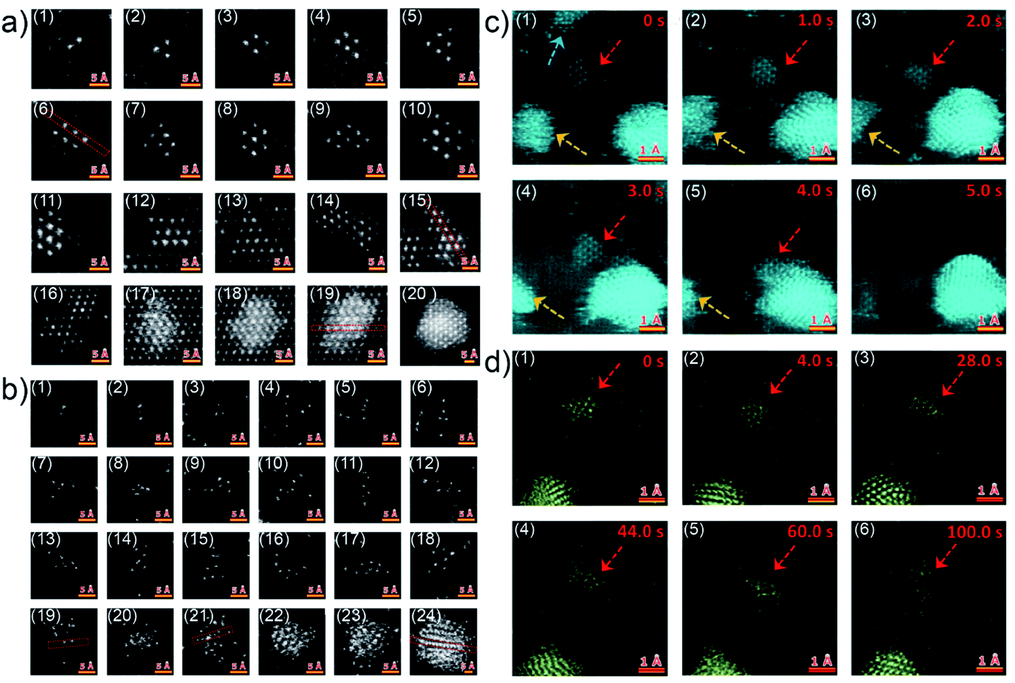 | ||
| Fig. 2 HAADF-STEM images of Au nanoclusters on (a) MgO (110) substrate and (b) amorphous carbon support. Two sequences of atomic-scale HAADF-STEM images of Au nanoclusters on (c) MgO (110) substrate and (d) amorphous carbon support, respectively. Reproduced with permission.40 Copyright 2017 American Chemical Society. | ||
Besides the mentioned fundamental studies about growth behaviors of Au clusters on solid substrates assisted with advanced characterization techniques, other fundamental investigations of UTGLs were also achieved, including revealing optical and structural properties of UTGLs,35,36 studying the effects of modification strategies (functionalized molecular monolayer, metallic surfactants/seeds) for substrates on the formation of UTGLs,22,37–39,44 as well as the effects of environmental factors (temperature, plasma, ultraviolet (UV) treatment) on the formation of UTGLs.42,43,45 For example, L. Leandro et al. used amino- and mercaptosilanes to modify a Si wafer to increase its adhesion for Au, obtaining smooth UTGLs with the average thickness below 10 nm and the average roughness below 5%.22 In detail, cleaned Si wafers were immersed (less than 3 h) in different solutions, including (3-mercaptopropyl)trimethoxysilane (MPTMS, 95%), (3-(2-aminoethylamino)propyl)trimethoxysilane (AEAPTMS, 80%), (3-aminopropyl)triethoxysilane (APTES, 99%), and (3-aminopropyl)trimethoxysilane (APTMS, 97%). After that, Au was deposited on the four treated Si substrates as well as a pristine Si substrate by using an E-beam evaporation system with a rate of 9.5 Å s−1, achieving 6 nm-thick deposited Au layers on all substrates. As presented by the scanning electron microscopy (SEM) images in Fig. 3(a), compared to the pristine Si substrate (Fig. 3(a1)), all four silanes-treated Si substrates (Fig. 3(a1)–(a5)) exhibited obviously an increased adhesion for the deposited Au. Especially, the Au layer formed on the fourth sample (Fig. 3(a5)), treated by APTMS, presented the most smooth and continuous morphology among these sample. Confirmed with atomic force microscopy (AFM) measurements, the surface roughness of this 6 nm-thick Au layer was below 0.26 nm with a root mean square (RMS) of 0.19 nm. Moreover, on a Si substrate treated by APTMS, a smooth and complete Au layer could be formed with a deposited thickness of 5 nm. As shown in Fig. 3(a6), such enhanced adhesion of deposited Au on the Si substrate treated by silanes could be attributed to that these silanes can form bonds between the deposited Au and the natural oxide layer on the surface of Si substrate. A. Kossoy et al. prepared UTGLs by evaporating Au onto silica (SiO2) substrates treated by MPTMS and studied the corresponding optical responses.35 A continuous and void-free Au layer was realized with the deposition thickness as low as 5.4 nm. The measured optical transmission spectra (thick black lines) of prepared UTGLs with the thicknesses of 3.0 nm, 4.2 nm, 5.4 nm, and 7.2 nm were demonstrated as shown in Fig. 3(b). However, the intensities of all measured data were lower than the theoretical values (thin black lines). Regarding the samples with continuous Au layer (5.4 nm and 7.2 nm), the measured data were well-matched with the modelling results (red lines) based on a three-layer model. This model considered a diffusion layer on the top of deposited Au layer and an interface layer between the substrate and deposited Au layer, as shown in the bottom area of Fig. 3(b3) and (b4). For the samples before the percolation threshold (3.0 nm and 4.2 nm), the separated Au clusters formed due to coalescence, as shown in the SEM images inserted in Fig. 3(a1) and (a2), could provide additional plasmonic absorption, leading to the mismatch between the measured data and the theoretical values (where the subjects were considered as continuous Au layer when calculating the theoretical values). This conclusion was also demonstrated by the results of finite-difference time-domain (FDTD) simulations, as indicated by the blue lines. This work provided new understanding about the optical properties of UTGLs by considering the diffusion layer on the top of Au and the transitional regime between Au and substrate.
 | ||
| Fig. 3 (a) SEM images of 6 nm-thick Au layers deposited on (a1) pristine Si substrate, and Si substrates treated by (a2) AEAPTMS, (a3) MPTMS, (a4) APTES, and (a5) APTMS. (a6) Simple scheme of mechanism of enhanced adhesion of deposited Au on the Si substrate treated by silanes. Reproduced with permission.22 Copyright 2015 American Chemical Society. (b) Measured (thick black lines), modelled (red lines), theoretical (thin black lines), FDTD-simulated (blue lines) optical transmission spectra of UTGLs with the thicknesses of (b1) 3.0 nm, (b2) 4.2 nm, (b3) 5.4 nm, (b4) 7.2 nm, respectively. Inset: SEM images of the samples with 3.0 nm Au layer and 4.2 nm Au layer, as well as the scheme of established three-layer model inserted in the corresponding panels. Reproduced with permission.35 Copyright 2014 WILEY-VCH Verlag GmbH & Co. KGaA, Weinheim. (c) Scheme of revised adhesion layer model for Ti/Au and Cr/Au multilayer systems. Reproduce with permission. Copyright 2017 American Chemical Society. (d) SEM images of 5 nm-thick UTGLs deposited on fused-SiO2 substrates with the substrate temperatures of (d1) 23 °C, (d2) 0 °C, (d3) −30 °C, (d4) −50 °C, (d5) −80 °C, (d6) −120 °C, and (d7) −195 °C, respectively. (d8) SEM image of 3 nm-thick UTGL prepared at −195 °C. (d9) Parameter uniqueness verification of the thickness of 3 nm-thick UTGL prepared at −195 °C. The dashed line denotes the best-fit Au layer thickness value of 2.95 nm. Reproduced with permission.43 Copyright 2019 American Chemical Society. | ||
Preparing a thin adhesion or seed layer, commonly using titanium (Ti) and chromium (Cr), on the substrate is another effective strategy to facilitate the formation of UTGLs.37,39 For example, M. Todeschini et al. investigated the influence of Ti and Cr adhesion layers on UTGLs with the thickness of 2–20 nm.37 The adhesion layers and Au layers were evaporation-deposited with a tunable thickness on SiO2 or silicon nitride (Si3N4) substrates for different characterizations. 2-Au, 20-Au, 2-Ti/2-Au, 2-Ti/20-Au, 2-Cr/2-Au, 2-Cr/20-Au films (the number represent the thickness (nm) of corresponding layer) were prepared, and their surface structures, interfacial structures, and compositions were systematically studied by TEM, SEM, AFM, energy-dispersive X-ray spectroscopy (EDX), electron energy-loss spectroscopy (EELS), and X-ray photoelectron spectroscopy (XPS) measurements. Based on such comprehensive analysis, the mechanism of how the Ti and Cr adhesion layers affect the growth of UTGLs were revealed, as illustrated by Fig. 3(c). During the formation of the adhesion layer (Fig. 3(c1) and (c2), deposited Ti or Cr atoms firstly nucleated and gradually grew to form an amorphous layer. Both, Ti and Cr, were partially oxidized by oxygen (O2) and water (H2O) molecules, which existed on the substrate surface and environment. During the Au deposition, the adhesion layer works as a wetting layer that can decrease the nucleation energy barrier and increase the number of nucleation sites, leading to a faster formation of a continuous Au layer compared to the scenario of depositing Au on a pristine SiO2 substrate. The development of Ti–Au and Cr–Au chemical bonds resulted in an enhanced wetting process. As shown in Fig. 3(c3), the existence of an adhesion layer facilitated the formation of UTGLs with a more monodisperse grain size and [111] crystal orientation. In terms of Cr adhesion layer, a Cr–Au alloy layer was formed during the initial deposition of Au (2–3 nm), leading to more Au loading to form Au layers compared to the case of a Ti adhesion layer. Moreover, with the same Au deposition thickness, the electrical conductivity of Ti/Au system was increased compared to pure Au layer, while the conductivity of Cr/Au stack was decreased. This could be attributed to the film parallel resistor behavior of Ti/Au system and the formation of an alloy layer within Cr/Au interface.
Regarding the effects of environmental factors on UTGLs, R. Lemasters et al. studied how the cryogenic temperatures affect the formation of UTGLs without adhesion or wetting layers.43 UTGLs with the thickness of about 5 nm were sputter-deposited on fused-SiO2 substrates with substrate temperatures ranging from 23 °C to −195 °C. Such cryogenic conditions were realized by installing a liquid nitrogen flow tube inside the magnetron sputter chamber. The surface morphology of these UTGLs prepared at 23 °C, 0 °C, −30 °C, −50 °C, −80 °C, −120 °C, and −195 °C were presented in Fig. 3(d1)–(d7). It was clearly observed that the cracks and voids in the deposited Au layers were reduced with decreasing the substrate temperature. When the substrate temperature was decreased to −195 °C, a continuous Au layer was achieved with the deposition thickness of 5 nm. This could be attributed to the low temperature of the substrate, which decreased the diffusion rate of deposited Au atoms and the surface mobility of formed Au small clusters, leading to a suppression of the 3D growth mode and a faster formation of percolated UTGL compared to the process at room temperature. In addition, the authors also prepared a 3 nm-thick Au layer on fused-SiO2 substrate at the temperature of −195 °C, as shown in Fig. 3(d8). Compared to the 5 nm-thick Au layer, although there were defects within the 3 nm-thick Au layer, it still exhibited a quasi-continuous morphology. The more accurate thickness of this Au layer was determined as 2.95 nm by spectroscopic ellipsometry. Moreover, the uniqueness of the achieved record-small thickness of 2.95 nm was verified by the calculations of regression-analysis-fitting mean-squared-error (MSE) in ellipsometry. As presented in Fig. 3(d9), the minimum of MSE curve was well matched with the thickness value of 2.95 nm, indicating the reliability and uniqueness of this thickness value.
2.2 On soft substrates
Depositing UTGLs on various polymer thin films has been regarded as a key step to achieving flexible and transparent sensors and devices, including organic photovoltaics (OPV), organic field effect transistors (OFET), and organic light-emitting diodes (OLED).68–73 In recent years, the in situ GIXS technique, as a powerful tool, attracted much attention to probe the morphology and structure evolutions of metal–polymer interfaces due to its non-destructive and real-time monitoring properties.30Poly(N-vinylcarbazole) (PVK) attracted much interests as the hole transport layer (HTL) for OPVs because of its thermal and chemical stability.74–76 In order to reveal the interaction mechanism at the metal–polymer (Au–PVK) interface during the electrode fabrication, G. Kaune et al. applied in situ GISAXS, for the first time, to study the growth behavior of sputter-deposited Au on a PVK thin film.48 The selected 2D GISAXS patterns obtained after a step-wise Au sputter deposition on PVK thin film are presented in the upper row of Fig. 4(a). A clear smaller-qy shift of the side peak was observed, which was related to the growth of the deposited Au clusters and the increase of the cluster correlation distance. For a further analysis, simulations of the obtained scattering patterns were performed by using the IsGISAXS software.77 In the model, two particle-types were chosen, which had a parallelepiped geometry and a spheroid geometry, in which each particle type was described with radius (r), radius distribution width (σ), and height (h) based on the distorted-wave Born approximation (DWBA) and the assumption of graded interfaces in the perturbated state caused by the particles.78,79 Gaussian shapes of the distribution functions were assumed for all distribution, while the interference function was calculated based on the 1D paracrystal model with the correlation distance (D) and disorder parameter (ω). The corresponding simulated GISAXS patterns are displayed in the lower row of Fig. 4(a), which showed a good agreement with the experimental data. The extracted evolution of the Au cluster h (parallelepiped geometry), r, and D are shown in Fig. 4(b). The r and D exhibited an approximately linear increase and displayed higher increase rates when the Au effective thickness was larger than 1.5 nm. This behavior was attributed to that the deposited Au clusters started to coalesce and connect with each other instead of adsorbing the adatoms for lateral growth, leading to the faster growth of the cluster size and the correlation distance. Besides, the height h displayed a nonlinear growth until the Au effective thickness reached 9 nm, demonstrating the 3D growth mode with pronounced height growth. In order to achieve more in-depth understanding of Au–PVK interface formation, an additional X-ray reflectivity (XRR) measurement was performed at a PVK film with 25 nm-thick Au deposition. As shown in Fig. 4(c), the result indicated that a small amount deposited Au diffused into the PVK film to formed an enrichment layer with a thickness of 1.2 nm and a mass density of 2.4 g cm−3.
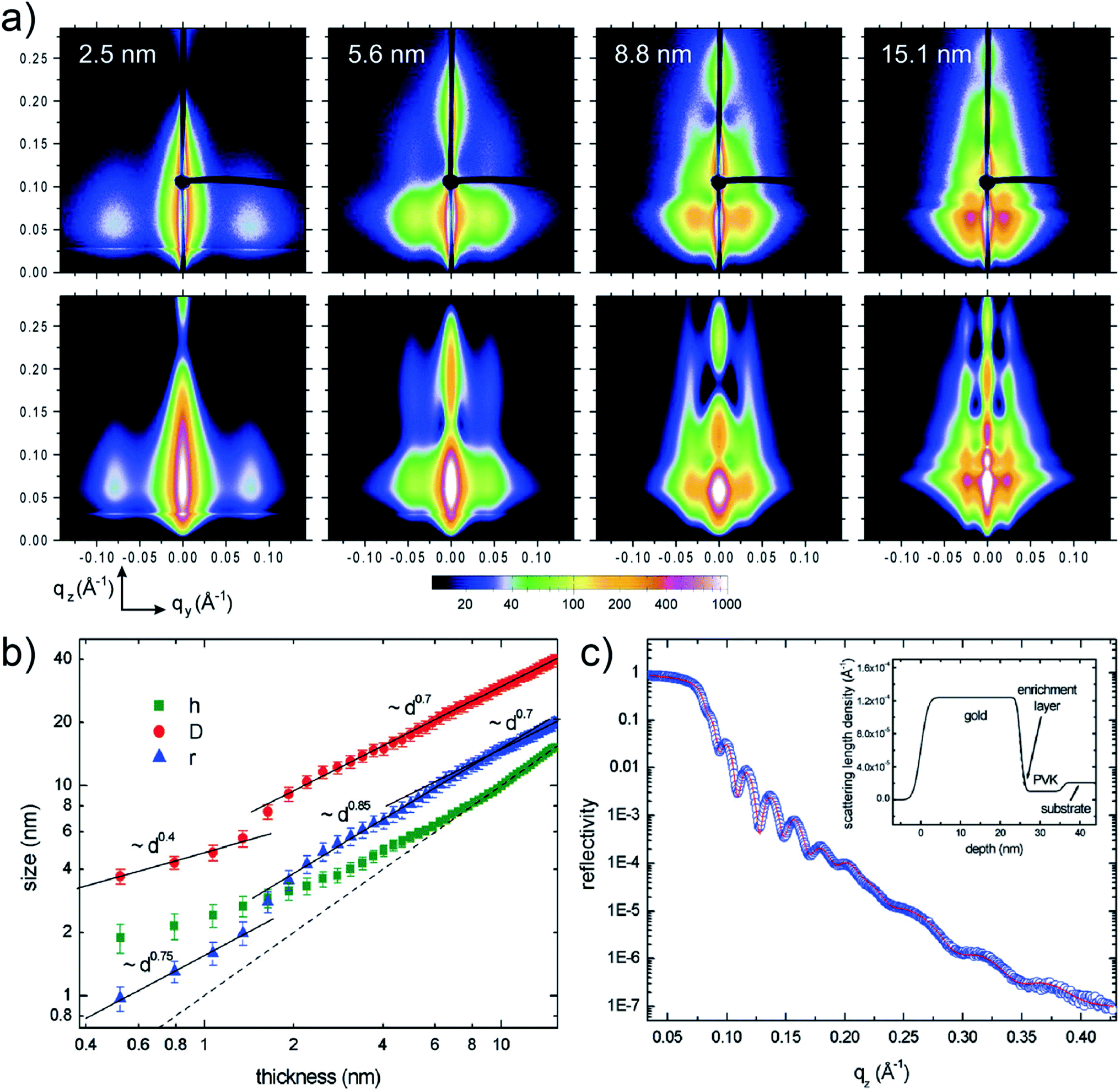 | ||
| Fig. 4 (a) Measured (upper row) and corresponding simulated (lower row) 2D GISAXS data when sputter-depositing Au on a PVK thin film with different Au effective thicknesses as indicated. (b) Extracted evolution of the Au cluster height h (parallelepiped geometry), radius r, and correlation distance D with the Au effective thickness. The dash line refers to the Au effective thickness. (c) Measured (circles) and fitted (line) XRR data of the PVK thin film with a 25 nm-thick deposited Au layer. The inset presented the scattering length density derived from the fit including a 1.2 nm-thick enrichment layer. Reproduced with permission.48 Copyright 2009 American Chemical Society. | ||
M. Schwarzkopf et al. investigated the basic principles of metal–polymer interface formation when sputter-depositing Au on polystyrene (PS) thin film by in situ GISAXS.49 The growth process of sputter-deposited Au cluster on PS thin film was presented by the mapping of both out-of-plane (horizontal direction, along qy) and off-detector (vertical direction, along qz) line cuts of obtained 2D GISAXS data at corresponding interested regions (seen in the captions), as shown in Fig. 5(a) and (b), respectively. In Fig. 5(a), the presence of distinct growth regimes of sputter-deposited Au was obviously revealed by a non-monotonous shift of the side peak location (qy,1) toward lower qy values. In Fig. 5(b), the bottom arrow indicated the shift of Yoneda peak, which was related to the accumulation of deposited Au. Besides, the shifts of intensity maxima towards lower qz values, indicated by the upper arrows, were caused by the thickness increase of deposited Au layer. Based on the before developed geometrical model mentioned in Section 2.1, the real-space parameters related to the deposited Au cluster growth on PS were calculated and the corresponding growth stages were described quantitatively, as presented by Fig. 5(c) and (d). The stage (I) was related to the nucleation and small clusters formation. At the beginning of the second stage (IIa), the inter-cluster distance, D, fast increased due to the coalescence of small cluster and then increased with a lower rate due to the restricted mobility of clusters in stage (IIb). In stage (III), the increase of D exhibited a similar trend (first fast, then slow) with that in stage (II). After reaching the percolation threshold, in stage (IV), the increase of D tended to be linear, indicating the layer growth along vertical direction. Moreover, regarding the evolution of decoupled cluster height (H) and radius (R), it was concluded that the cluster growth followed a changeable aspect ratio between H and R in the first 3 nm deposition, and then the growth kept a nearly constant aspect ratio during the later deposition. Moreover, molecular dynamic simulations also exposed excellent agreement for the extracted morphological parameters within the first 3 nm of Au growth during sputter deposition.80 The value of 2R/D exhibited a continuous increasing trend until δAu = 1.9 nm, where the value presented a local maximum. This was attributed to that the inter-cluster distance increased faster than the cluster growth due to partial coalescence of previously isolated small clusters, resulting in the release of initially covered surface area and a far faster drop in cluster density. The percolation threshold was reached at δAu = 5.2 nm when the extracted 2R was equal to D. Moreover, the evolution of contact angle (CA) of the deposited Au clusters were also obtained based on the information about H and R. CA was smaller than 180° after δAu = (0.38 ± 0.03) nm and displayed an ever-decreasing trend during the later deposition process, reaching CA = (92 ± 1)° at δAu = 1.9 nm. This was attributed to changes of interfacial energy γAu/PS at the early stage of sputtering and the formation of elongated domains due to coalescence in the following deposition process.
 | ||
| Fig. 5 Mappings of (a) out-of-plane line cuts (at the PS Yoneda peak of qz = 0.69 nm−1) and (b) off-detector line cuts (at qz = 0 nm−1, 0.187 nm−1 < qy < 2.852 nm−1) of 2D GISAXS data versus deposited Au effective thickness. (c) Evolution of inter-cluster distance D (black), cluster radius R (red), and cluster height H (blue). (d) Evolution of cluster diameter over distance ratio 2R/D (blue), cluster density ρ (red), and contact angle CA (green). Reproduced with permission.49 Copyright 2015 American Chemical Society. Evolution of inter-cluster distance D and cluster radius R at different sputter powers of 3 W (black), 14 W (red), 25 W (blue), 50 W (magenta), and 100 W (green) in the (e) first 2 nm and (f) first 8 nm effective thickness, respectively. Evolution of (g) cluster diameter over distance ratio 2R/D and (h) cluster density ρ at different sputter powers of 3 W (black), 14 W (red), 25 W (blue), 50 W (magenta), and 100 W (green). Reproduced with permission.51 Copyright 2017 American Chemical Society. | ||
Also, by M. Schwarzkopf et al., the role of sputter deposition rate for the growth and structure of Au when depositing Au on PS thin films was studied based on the analysis of in situ GISAXS data.51 The sputter deposition rate (J) was controlled by tuning the sputter power (P). The studied samples in this work were prepared under P = 3 W, 14 W, 25 W, 50 W, and 100 W, corresponding to J = (0.041 ± 0.002) nm, (0.201 ± 0.008) nm, (0.366 ± 0.015) nm, (0.73 ± 0.03) nm, and (1.51 ± 0.08) nm, respectively. The growth behaviors of sputter-deposited Au on PS thin films under the different deposition rates were also probed by analyzing the in situ GISAXS data with the geometrical model. Fig. 5(e) and (f) show the evolution of D and R of deposited Au clusters under different deposition rates. In the first 2 nm deposition (Fig. 5(e)), it could be observed that the deposition rate affected the nucleation processes (stage I). In stage II, the evolutions of both D and R exhibited similar trends with the different deposition rates, indicating that the effect of deposition rate on the diffusion-mediated growth processes was negligible. During the following stage (III), the adsorption-mediated growth, the effect of deposition rate on the evolution of D started to be obvious. For the depositions at lower rates (P = 3 W and 14 W), the correlation distance D increased much faster than the cluster radius R, indicating that the deposited clusters tended to form local dimers. In the cases with higher rates, such onset of partial coalescence was not observed. With higher deposition rates, more small clusters could form fast and they had stronger adsorption with each other, leading to the formation of elongated, branched domains instead of dimers. As shown in Fig. 5(g), the evolution trends of 2R/D values at lower deposition rates (P = 3 W and 14 W) were similar with that the last work mentioned above. The local maximum at about δAu = 1.6 nm were observed due to the partial coalescence. With higher deposition rates, such phenomenon was not pronounced anymore. The percolation thresholds were reached at δAu = (6.3 ± 0.3) nm, (5.3 ± 0.2) nm, (4.2 ± 0.2) nm, (3.7 ± 0.2) nm, and (3.4 ± 0.2) nm under P = 3 W, 14 W, 25 W, 50 W, and 100 W, respectively. Thus, changing the sputter power turned out to be a very easy way to reach percolation at lower deposited Au amount. As presented in Fig. 5(h), the cluster density ρ decreased reasonably with the increase of deposition rate, due to the easier formation of elongated domains.
Up to now, various works about using in situ GISAXS technique to probe the growth kinetics of UTGLs on different substrates have been reported, and such technique has exhibited promising prospects in this research field. However, due to limited time resolution, it was always challenging to reveal the nucleation and small-cluster growth processes in the very beginning of Au deposition especially at industrial-relevant deposition rates by using in situ GISAXS approach. In order to address this issue, most recently, M. Schwarzkopf et al. applied next-generation X-ray detectors to observed the initial growth of sputter-deposited Au cluster on PS thin film by sub-millisecond in situ GISAXS whose time resolution was as high as 0.5 ms (2000 fps).58 The sputter deposition process with an effective Au deposition rate of 1.52 nm s−1 on PS thin film in the first 4 nm effective Au thickness was recorded (2000 frames per second) and analyzed in detail. Fig. 6(a) presents the temporal evolution of the intensity distribution along the reflection plane as a function of exit angle I(αf, t), which indicated the electron density distributions parallel to the sample surface. The contour plots of out-of-plane and off-detector line cuts of 2D GISAXS patterns as a function of effective Au thickness (dAu) are shown in Fig. 6(b) and (c). The lower-qy shift of the side peak location (qy,2), driven by the growth of deposited Au clusters, was clearly observed as seen in Fig. 6(b). The arrows marked in Fig. 6(a) and (c) indicate the evolution of X-ray thin film interferences (XTFI) peak positions which shifts towards higher scattering angles (qz values). This was related to an increase of the layer dispersion of the PS substrate (δPS) and a simultaneous decrease of the correlated interface distance (dPS). As shown in Fig. 6(d), such variation could be indicated by the average volume fraction of Au in PS layer (fAu), which could be calculated by the relation fAu(δPS) ≈ (δPS(t) − δPS,0)/(δAu − δAu,0). The value of fAu increased fast in the first second of sputtering deposition due to the sub-surface diffusion of adatoms and then increased moderately because of growing Au clusters trapping the free adatoms. Meanwhile, the correlated PS layer thickness (dPS) reduced from ca. 88 nm to lower than 85 nm. Moreover, the evolution of extracted average inter-cluster distances D, cluster radii R, and cluster heights H as a function of dAu are presented in Fig. 6(e), while the evolution of height to radius aspect ratio H/R, average cluster density ρ, and number of atoms per cluster NAu as a function of time (t) are displayed in Fig. 6(f). Based on these parameters, the four-stage growth model of sputter-deposited Au on a solid substrate was refined, especially with respect to the in-depth exploration of the Au–PS interfacial morphology in the very beginning of sputter deposition. In the stage (I), the inter-cluster distance D decreased slightly due to the formation of new nuclei, which was neglected in the previously studies. The sub-stage (Ia) was related to landing, accommodation, and collisions of adatoms within microseconds, which was beyond the resolution of the used setup. When t = 0.5 ms, the first deduced values of D, R, H were around (3.8 ± 1.5) nm, (0.17 ± 0.04) nm, and (0.53 ± 2.08) nm, respectively. Compared with the Au atomic radius 0.144 nm, it could be speculated that single Au adatoms and vertical Au2 dimers were the dominated species and structures after 0.5 ms of deposition. The abundance of vertical dimers also caused the high aspect ratio H/R. These Au2 vertical dimers had been theoretically predicted by density functional theory (DFT) to be the most stable configuration.81,82 In the following sub-stage (Ib), the planar ultra-small cluster, vertical dimers, and adatoms tended to coalesce to form larger clusters, leading to the fast decrease of aspect ratio H/R and the increase of number of atoms per cluster NAu. Besides, the cluster density ρ almost remained constant in this regime, indicating the high mobility and coalescence capability of formed ultra-small clusters. The aspect ratio H/R and cluster density ρ both exhibited temporary increasing trends in stage (Ic), which could be attributed to the formation of truncated-spherical clusters. In the following diffusion-mediated stage (II), adsorption-mediated stage (III), and layer growth stage (IV), the growth behavior was similar with obtained growth laws according found in earlier studies. The percolation threshold was reached around dAu = 3.5 nm in this work.
 | ||
| Fig. 6 Contour plots of (a) temporal evolution of the intensity distribution along the reflection plane, (b) out-of-plane and (c) off-detector line cuts of 2D GISAXS patterns as a function of dAu. (d) Temporal evolution of filling factor fAu (black) and correlated thickness of PS layer dPS (red). (e) Evolution of average inter-cluster distances D (black), cluster radii R (red), and cluster heights H (blue) along with dAu. (f) Temporal evolution of height to radius aspect ratio H/R (black), average cluster density ρ (red), and number of atoms per cluster NAu (blue). Reproduced with permission.58 Copyright the Royal Society of Chemistry 2021. | ||
To be more relevant to practical applications, more application-oriented in situ researches were done in recent years, aiming to use in situ GIXS technique to study the Au–polymer interface formation for OPVs and perovskite solar cells (PSCs). In particular, F. C. Löhrer et al. studied and compared the formation processes of Au contact on the low band gap polymer poly({4,8-bis[(2ethylhexyl)oxy]benzo[1,2-b:4,5-b′]dithiophene-2,6-diyl}{3-fluoro-2-[(2-ethylhexyl)carbonyl]thieno[3,4-b]thiophenediyl}) (PTB7) and poly[4,8-bis(5-(2ethylhexyl)thiophene-2-yl)benzo[1,2-b:4,5-b′]dithiophene-2,6diyl-alt-(4-(2-ethylhexyl)-3-fluorothieno[3,4-b]thiophene)-2carboxylate] (PTB7-Th) thin films, respectively, using in situ GISAXS and in situ grazing incidence wide-angle X-ray scattering (GIWAXS).52 The crystallinity of sputter-deposited Au layers on the both polymer films was presented by the vertical cake cuts of the 2D GIWAXS data as shown in Fig. 7(a1) for PTB7 and Fig. 7(a2) for PTB7-Th, respectively. In both cases, two visible Bragg peaks were observed at 2.676 Å−1 and 3.088 Å−1, corresponding to the (111) peak and (200) peak of face-centered cubic Au crystallites. In addition, the evolution of the (111) peak position (q) and full width at half-maximum (FWHM) with the increase of Au effective thickness are presented in Fig. 7(a3) and (a4), respectively. As a result, the crystallinity of deposited Au was not affected by the different polymer thin films. The growth processes of deposited Au on the both polymer films were revealed by the analysis of in situ GISAXS data based on the geometry model established by M. Schwarzkopf et al. mentioned above. The overview of Au growth processes on PTB7 and PTB7-Th films were displayed by the horizontal line cuts of GISAXS patterns and the evolutions of extracted center-to-center cluster distance D with the Au effective thickness, as shown in Fig. 7(b). Furthermore, a more detailed Au growth behavior was described by the extracted average cluster radius R, ratio of the average cluster diameter to cluster distance 2R/D, surface coverage θ, cluster density ρ, and number of gold atoms per cluster NAu/cluster, as shown in Fig. 7(c). Based on the analysis, on the both of PTB7 and PTB7-Th thin films, the deposited Au exhibited similar growth process. However, the differences were still distinguished by these extracted parameters, especially during the early stage (stage I and II) of the deposition. For example, as shown in Fig. 7(c2), the variation of the 2R/D ratio and θ for PTB7-Th displayed more pronounced plateauing compared to the case on PTB7. This difference could be related to the reduced mobility of deposited Au clusters on the PTB7-Th film due to the introduction of side chains.
 | ||
| Fig. 7 (a) Evolution of the crystallinity of the deposited Au presented by the integrated vertical cake cuts (azimuthal angle χ from −15° to 15°) of the 2D GIWAXS data for (a1) PTB7 (blue) and (a2) PTB7-Th (red). Evolution of (a3) (111) peak position and (a4) FWHM with the Au effective thickness for PTB7 (blue) PTB7-Th (red). (b) Horizontal line cuts of 2D GISAXS data and corresponding fits (black curves) for (b1) PTB7 (blue) and (b2) PTB7-Th (red). (b3) Evolution of center-to-center cluster distance D with the Au effective thickness for PTB7 (blue) and PTB7-Th (red). (c) Evolution of the extracted average cluster radius R, center-to-center cluster distance D, ratio of the average cluster diameter to cluster distance 2R/D, surface coverage θ, cluster density ρ, and number of gold atoms per cluster NAu/cluster with the Au effective thickness for PTB7 (blue) and PTB7-Th (red). Reproduced with permission.52 Copyright 2019 American Chemical Society. | ||
Regarding the PSC applications, L. Song et al. reported an in situ study of sputtering Au films on 100 nm-thick 2,2′,7,7′-tetrakis(N,N-bis(p-methoxyphenyl)amino)-9,9′-spirobifluorene (spiro-OMeTAD) films.56 The growth kinetics of the deposited Au contact on the spiro-OMeTAD film was revealed by the in situ GISAXS data and corresponding analysis and simulations. As a result, four different regimes of the deposited Au growth were categorized as (I) lateral growth, (II) coarsening, (III) complete layer formation, and (IV) vertical growth. It should be noted that the XRR measurement results and corresponding fits indicated that the deposited Au atoms could diffuse into the spiro-OMeTAD film, resulting in the formation of an enrichment layer with a thickness of 3.5 nm and a mass density of 2.9 g cm−3. Such Au doping of spiro-OMeTAD occurred at the initial stage of sputter deposition and could cause an influence on the final performance of PSC devices.
2.3 On nanostructured substrates
When moving from homopolymer to diblock copolymer films as substrates for the Au sputter deposition, also a templating effect adds to the process of Au growth due to the nanostructure of the diblock copolymer film. E. Metwalli et al. studied with in situ GISAXS Au sputter deposition onto a nanostructured polymer template, which was established from a mixture of polystyrene-block-polyisoprene-block-polystyrene P(S-b-I-b-S) triblock and polystyrene-block-polyisoprene P(S-b-I) diblock copolymers.59 The PS spheres were arranged in a liquid-like type with a well-defined nearest neighbor distance inside a PI matrix acting as a template for directing the Au atoms during the sputter deposition. Interestingly, such type of polymer mixture is used in pressure sensitive adhesive (PSA) applications. The obtained 2D GISAXS data each obtained after repetitions of 6 s sputter deposition of Au on the blend copolymer thin film are shown in Fig. 8(a). In Fig. 8(a1), for the pristine blend copolymer thin film two prominent peaks (at ±0.015 Å−1, marked with arrows) were clearly observed, which originated from the interference by PS domains. With ongoing sputter deposition, the intensities along qz of prominent peaks gradually increased, and two soaring increases of the scattering intensities on both sides of the beam stop (qy < 0.006 Å−1) were also observed, due to the accumulation of deposited Au. As shown by the horizontal line cuts of the 2D GISAXS data and corresponding fits (Fig. 8(b)), both position and intensity of the prominent peak remained almost constant during the sputter deposition, and no other peaks was observed. This behavior indicated that the deposited Au diffused into the polymer film instead of existed on the film surface. Besides, the plot of vertical line cuts (Fig. 8(c)) displayed a gradual increase of the intensity due to the increased amount of deposited Au. Moreover, the polymer film with 4.3 Å-thick deposited Au was kept to relax for 10 h, followed by the investigation via GISAXS. The corresponding 2D GISAXS data, horizontal and vertical line cuts for this relaxed Au/polymer film are shown in Fig. 8(a12), the top line in Fig. 8(b), and the top line in Fig. 8(c), respectively. The results indicated that the Au decorated polymer film exhibited a stable morphology after 10 h relaxation. After a comprehensive investigation, this study concluded that the sputter-deposited Au tended to diffuse into both of the PS and PI regions and decorated the PS domains. In the PS regions, the Au–Au interaction overwhelmed the Au–polymer interaction, while the Au–Au interaction was suppressed in the PI regions due to the reduced mobility of deposited Au capped by the delocalized π-bonded electrons on PI chains.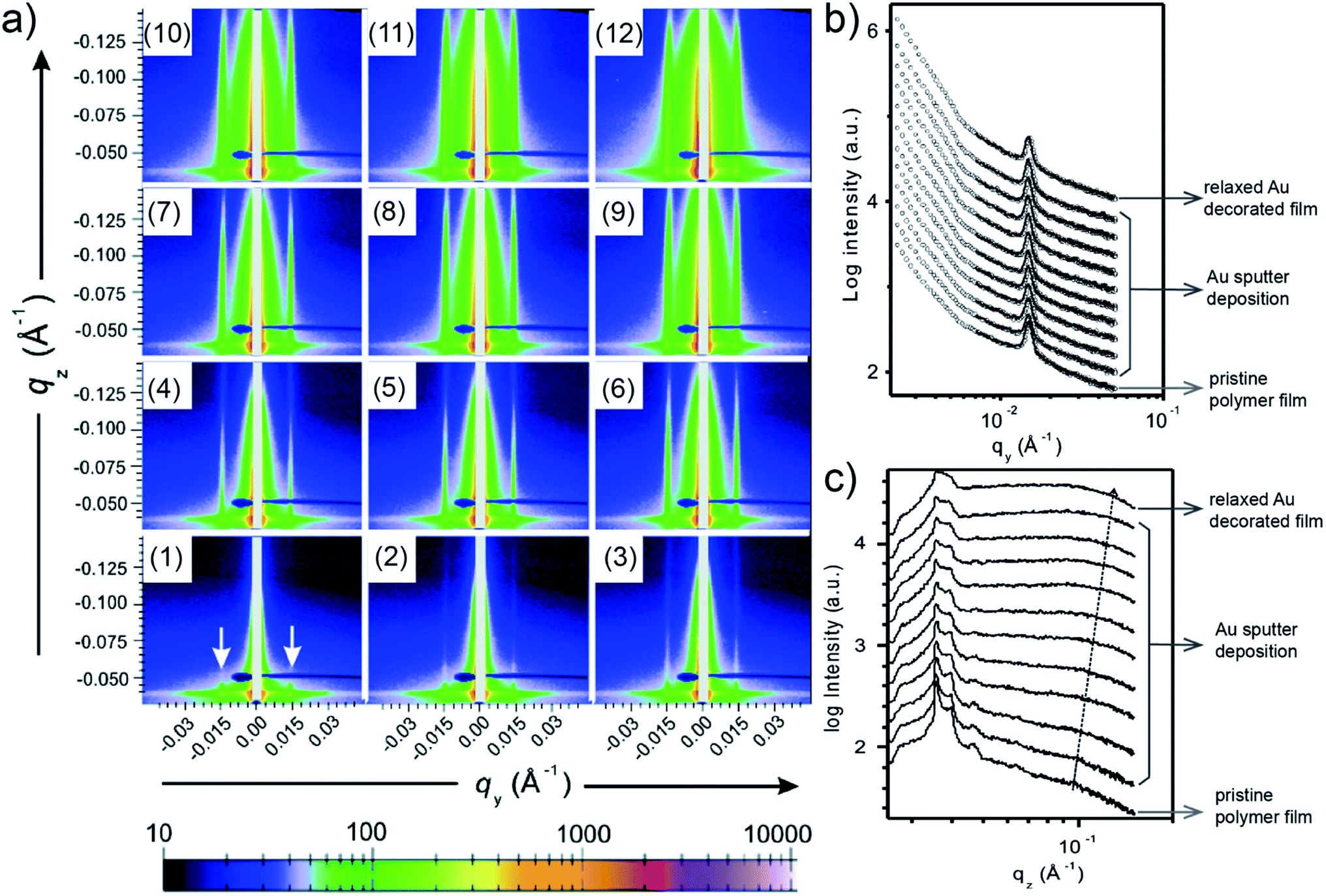 | ||
| Fig. 8 (a) 2D GISAXS data of (a1) pristine phase-separated polymer thin film, (a2)–(a11) 10 repetitions of 6 s sputter deposition onto the polymer film, and (a12) polymer film with 4.3 Å-thick deposited Au after 10 h relaxation. (b) Horizontal and (c) vertical line cuts of the 2D GISAXS data. Reproduced with permission.59 Copyright 2008 American Chemical Society. | ||
Due to a broad absorption spectrum range, quantum dots (QDs) are regarded as one of the most promising candidates for achieving long-wavelength electronic devices, including LEDs,83,84 solar cells,85,86 and photodetectors.87,88 Generally, UTGLs or thin Au layers are deposited on QD arrays to act as electrode. Thus, the Au–QD interface is significant for the device performance because of the metal–semiconductor junction.89 Compared to the cases on the flat substrates, the growth behavior of deposited Au clusters on QD arrays with nanostructured surface can be expected to be more complex. In order to probe the formation process of the Au–QD interface, several efforts have been done to fundamentally study the growth processes of deposited Au on different QD arrays.60,62,64 In an initial in situ GISAXS study N. Paul et al. studied templating the growth of Au nanostructures with a CdSe quantum dot array.60 In a later study, W. Chen et al. applied in situ GISAXS to focus on the early stage of Au sputter deposition on a lead sulfide (PbS) QD solid.62 The first glance of the sputter-deposited Au growth process on PbS QD solid was depicted with the mappings of vertical and horizontal line cuts of in situ 2D GISAXS data, as presented in Fig. 9(a1) and (a2), respectively. The evolution of side peak H1 was related to the formation of small Au clusters (SCs) and subsequent growth with increasing the inter-cluster distance. When the effective Au thickness (δAu) reached 2 nm, the QDs exhibited a template effect for the Au growth, where the inter-cluster distance tended to converge towards the interdot distance of the QDs, leading to the emergence of an addition side peak H2. The grown-up Au clusters were defined as medium gold clusters (MCs) that were influenced by the QDs' boundaries. With ongoing deposition, such template effect by the QDs was weakened due to the continuous growth of the Au cluster. The third side peak H3 was featured by the increasing of formed large Au clusters (LCs). It should be noted that the peak positions of H2 and H3 almost remained unchanged from around δAu = 6 nm to the end of the Au deposition process, indicating that the final structure of sputter-deposited Au was mainly dominated by MCs and LCs with distinguished sizes and inter-structure distances. For the further quantitative analysis, the selected horizontal line cuts were modelled based on the framework of the DWBA applying the local monodisperse approximation and assumption of a 1D paracrystal arrangement of cylindrically shaped scattering objects,78,79 as presented by Fig. 9(a3). The extracted form factors (radii) and structure factors (inter-cluster distances) of MCs and LCs were shown in Fig. 9(a4) and (a5), respectively. The template effect of QDs was demonstrated by the slightly increased radius and almost constant inter-cluster distance of MCs during the deposition process, in which the inter-cluster distance of about 5.1 nm was well matched with the lattice distance of underneath QDs. To further investigation of QDs' template effect for Au growth in more detail, the obtained 2D GISAXS patterns were simulated by using the BornAgain software,90 as presented in Fig. 9(b). The original 2D GISAXS pattern at δAu = 2.5 nm was selected due to the strong template effect of MCs at that point of the sputter deposition process. In the assumed model, the MCs were assumed as spherical shape with a radius of 1.9 nm and an inter-cluster distance of 5.1 nm based on the initial line cut modelling, whereas the QDs were also modelled with a spherical shape with a radius of 2.4 nm and an interdot distance of 5.1 nm. Two different models with different stacking types between MCs and QDs were calculated. One model, as shown in Fig. 9(b4), was a positional-coupled type of arrangement where MCs were well located on the top of each QD. Another model, as shown in Fig. 9(b5), was a positional-decoupled configuration where the positions of top MCs and underneath QDs were non-correlated. By comparing the simulation results, as presented in Fig. 9(b2) and (b3), the positional-decoupled model (Fig. 8(b3)) was closer to the real scenario of QD template-induced Au growth with a weak position correlation seen in the GISAXS measurement. Based on the detailed analysis, the growth stages of sputter-deposited Au on PbS QD solid were well illustrated by the schemes in Fig. 9(c).
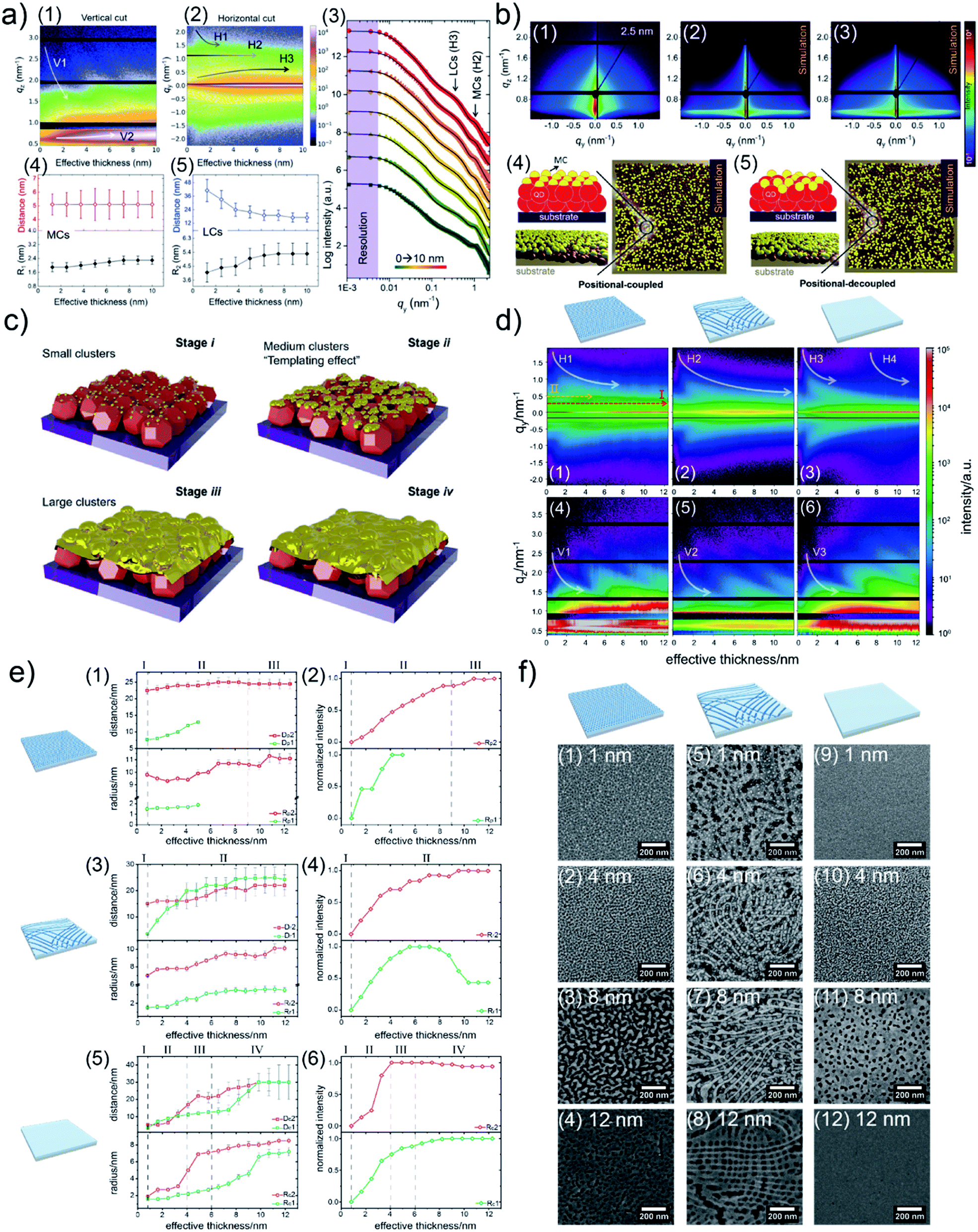 | ||
| Fig. 9 Mapping of (a1) vertical line cuts (at qy = 0 nm−1) and (a2) horizontal line cuts (at the critical angle of Au) of 2D GISAXS data as a function of effective Au thickness. (a3) Selected horizontal line cuts (colorful symbols) at different effective thicknesses with corresponding model results (black lines). Evolution of extracted inter-cluster distances and cluster radii of (a4) MCs and (a5) LCs as a function of effective Au thickness. (b1) Measured 2D GISAXS data at an effective thickness of 2.5 nm and (b2) simulated 2D GISAXS patterns based on the (b4) position-coupled model and (b3) simulated 2D GISAXS pattern based on the (b5) position-decoupled model. (c) Illustration of the different growth stages of sputter-deposited Au on PbS QD solid: (i) formation of small clusters, (ii) formation of medium clusters templated by the underneath QDs, (iii) formation and growth of large clusters, (iv) growth of Au layer along the vertical direction. Reproduced with permission.62 Copyright 2020 American Chemical Society. Mapping of horizontal line cuts as a function of effective Au thickness on (d1) porous TiO2, (d2) reticular TiO2, and (d3) compact TiO2 templates. The horizontal line cuts were taken at the region 0.59 nm−1 < qz < 0.63 nm−1. Mapping of vertical line cuts as a function of effective Au thickness on (d4) porous TiO2, (d5) reticular TiO2, and (d6) compact TiO2 templates. The vertical line cuts were taken at qz = 0 nm−1. Extracted inter-cluster distances (D) and cluster radii (R) a function of effective Au thickness when depositing Au on (e1) porous TiO2, (e3) reticular TiO2, and (e5) compact TiO2 templates. Extracted normalized intensities related to form factors of the modelled structures as a function of the deposited effective Au thickness when depositing Au on (e2) porous TiO2, (e4) reticular TiO2, and (e6) compact TiO2 templates. SEM images of Au/TiO2 hybrid thin films with (f1)–(f4) porous TiO2, (f5)–(f8) reticular TiO2, and (f9)–(f12) compact TiO2 templates, with different effective Au thicknesses as indicated. Reproduced with permission.63 Copyright 2021 American Chemical Society. | ||
Au/titanium (TiO2) hybrid nanomaterials have been applied in many fields, including plasmonic sensors, photocatalysis, and as advanced electron transport layers for solar cells.91–95 Based on advanced nanotechnology, TiO2 matrixes can be developed into various nanostructures for pursing an enhanced performance of the final devices. Therefore, regarding the preparation of Au/TiO2 hybrid nanomaterials by sputter deposition or evaporation strategies, it can be expected that the nanostructures of TiO2 matrixes or substrates could affect the growth behavior of Au during the deposition process. In order to reveal such effects, S. Liang et al. prepared TiO2 thin films with different morphology to act as templates for the Au sputter deposition, and investigated the growth processes of deposited Au on these different TiO2 substrates by using in situ GISAXS.63 Tuning the morphology of TiO2 thin films was realized by typical sol–gel synthesis, resulting in porous and reticular TiO2 thin films. Besides, a compact TiO2 thin films was also prepared as a reference. Overview of the sputter-deposited Au growth processes on the three different TiO2 substrates were outlined by the line cut mappings of the obtained 2D GISAXS data, as presented in Fig. 9(d). The emergences and lower-qy shifts of the side peaks H1, H2, and H3 indicated the formation of small Au clusters and growing processes on the porous, reticular, and compact TiO2 substrates, respectively. The peaks V1, V2, V3, and their analogues were also visible during the deposition due to the increased thickness of deposited Au layers. In particular, for the porous TiO2 substrate, a pseudo-Bragg peak (peak I) and a second-order peak (peak II) were visible since the beginning of deposition, which was attributed to the porous structure of TiO2 film. With ongoing deposition, the intensities of peak I and peak II gradually increased due to the growth of Au clusters along with the pore structure, indicating the template effect of the porous TiO2 substrate for the growth of sputter-deposited Au. When the effective Au thickness (δAu) reached around 5 nm, the peak II intensity tended to decrease, which indicated the gradual disappearance of the ordered Au structure guided by the porous TiO2 template due to the formation and further interconnection of large Au clusters at the late stage of Au deposition. Besides, peak H1 shifted towards lower qy values and then almost kept a stable position after δAu ≈ 7 nm, which also indicated the template effect of the pore structure for the Au growth. For the reticular TiO2 substrate, the lower-qy shift of the peak H2 continued until the end of the Au deposition process, which indicated the continuous increase of the inter-cluster distance as well as of the radius of the deposited Au clusters. This behavior was attributed to the larger surface structure of the reticular TiO2 substrate compared to the porous TiO2 film, resulting in a weaker template effect of Au growth within nanoscale local areas. Regarding the case of the compact TiO2 thin film, due to the absence of a pronounced surface nanostructure, the lower-qy shift of the peak H3 exhibited a shorted period (continued until δAu ≈ 4 nm) compared to the corresponding processes on the other two templates. When δAu ≈ 6 nm, another side peak H4 appeared and also exhibited a lower-qy shift trend, which indicated that granular structures with higher order were formed in the Au layer. The form factors and structure factors of the sputter-deposited Au clusters formed on the different TiO2 templates were extracted from the modelling results of selected horizontal line cuts based on the DWBA assumption, as displayed in Fig. 9(e1), (e3) and (e5). In Fig. 9(e1), the structure P1 (green symbols) and structure P2 (red symbols) were correlated to the growth of deposited Au clusters in the early deposition stage (featured by peak H1) and the template-induced growth of Au clusters (featured by peak I), respectively. When δAu > 5 nm, the features (Rp1, Dp1) of structure P1 could not be extracted from the modelling due to the strong contribution of Au clusters by templated-induced growth to the scattering. Meanwhile, both form factor (Rp2) and structure factor (Dp2) of structure P2 were almost constant because of the template effect of porous TiO2 substrate. Besides, the continuous increase in the intensity of Rr2 (Fig. 9(e2)) also indicated such gradually dominating template effect during the Au deposition. For the reticular substrate, as shown in Fig. 9(e3), it should be noted that Dr2 gradually increased and became larger that Dr1 when δAu > 4 nm, and then both Dr1 and Dr2 exhibited slightly increasing trends with close values. These findings indicated that after the inter-cluster distance of Au clusters increased to values larger than the interdistance of the nanowires within the reticular TiO2 substrate, the surface nanostructures of the reticular TiO2 film started to exhibit a template effect on the Au growth. Regarding the compact TiO2 substrate, due to the absence of a pronounced surface nanostructure, the form factors (Rc1, Rc2) and structure factors (Dc1, Dc2) increased and gradually stayed constant at the late stage of deposition (δAu > 10 nm), indicating the formation of a compact Au layer. The corresponding variations of form factor intensities with the Au growth on reticular TiO2 and compact TiO2 substrates are presented in Fig. 9(e4) and (e6), respectively. For more direct observations of the Au growth processes on the different TiO2 substrates, as well as for further applications, Au/TiO2 hybrid thin films based on the three TiO2 substrates with different effective Au thicknesses were prepared and measured by SEM, as presented in Fig. 9(f). The porous TiO2 substrate exhibited an obvious template effect for Au growth within nanoscale local areas, especially for a thin effective Au thickness (δAu = 4 nm). Due to the larger surface structure of the reticular TiO2 film, its template effect dominated larger-scale areas compared to that of the porous TiO2 film, leading to the remained network-like Au structures after the deposition of δAu = 12 nm.
3. Applications of ultra-thin gold layers
Based on those detailed and in-depth fundamental studies discussed in the last section, the general growth behavior of deposited Au on different substrates has been fully understood. In recent years, more and more applications based on UTGL configurations have been reported, including the examples from optical applications,6,7,96–106 electronic device applications,107–115 and as seed layers.116–1253.1 Optical applications
Due to the effects of localized surface plasmon resonances (LSPR) and surface plasmon resonances (SPR), UTGLs exhibit unique optical properties in the visible and the near-infrared (NIR) regions.126–129 The UTGL-based applications focusing on optical field include but are not limited to tunable optical responses or plasmons,6,7,96,98 plasmonic sensor,99,104 plasmonic printing,97 surface-enhanced Raman scattering (SERS),100,105 surface plasmon polariton (SPP) generation,101,106 and infrared absorber.102 The details of selected studies about these UTGL-based applications are summarized in Table 1.| Material composition | Au thickness/nm | Preparation method | Application | Ref. |
|---|---|---|---|---|
| Au/ZnO | 2.5–30 | Sputter deposition | Optical responses | 6 |
| TiO2/Au/TiO2 | 10.5 | Sputter deposition | Optical responses | 96 |
| Ag/Au | 6 | Evaporation | Optical responses | 7 |
| Au/Ag NWs | 5, 15 | Evaporation | Plasmonic printing | 97 |
| Au/Si | 0.5–10 | Evaporation | Optical responses | 98 |
| Au/TiO2 | — | — | Plasmonic sensor | 99 |
| Au/Si | 1.6–21.7 | ALD | SERS | 100 |
| MoS2/Au | 25 | Evaporation | Quantum emission | 101 |
| Au/CuxOy/SixNy | 2–13 | CVD | Infrared absorber | 102 |
| TMDS/Au/defective layer | 2.4–40 | — | 1D photonic crystal | 103 |
| Au/TiO2/SiO2 | 15–25 | — | SPR sensor | 104 |
| Au/Ag | 10 | Sputter deposition | SERS | 105 |
| Au/Ag | 10 | — | SPP wave excitation | 106 |
R. A. Maniyara et al. prepared UTGLs with few-nanometer thickness with the assistance of a Cu seed layer and realized tunable plasmons in the deposited UTGLs with different thicknesses.98 The Cu seed layer was first sputter-deposited on the Si substrate, followed by the sputter deposition of UTGLs. As shown in Fig. 10(a), compared to the unseeded UTGL (mass-equivalent thickness t ≈ 3 nm), the seeded UTGL formed a continuous and smooth morphology with the same thickness. In the visible-NIR transmission spectra, the unseeded UTGLs (Fig. 10(a3)) exhibited obvious minima around 600 nm when t < 7 nm, because of the LSPR effects originating from the isolated Au clusters. In contrast, the seeded UTGLs (Fig. 10(a4)) presented a decreasing trend of transmission at the NIR region when t exceeded 1 nm, indicating the long-range connection of the deposited Au layer. In order to achieve tunable plasmonic properties of the obtained UTGLs, nanoribbon structures were patterned on the UTGLs with a structural width W and a period P, as illustrated in Fig. 10(b1) and (b2). Both W and P could be controlled by electron beam lithography. The NIR-MIR (mid-infrared) transmission and reflection spectra of 3 nm-thick UTGLs with nanoribbon structures (with different W as indicated and P = 1.5 W) are presented in Fig. 10(b3). The obvious resonance peaks exhibited a red-shift trend when W was increased from 200 nm to 800 nm, which was also in good agreement with simulation results (dash lines). Moreover, the optical responses of 6 nm and 15 nm nano-patterned UTGLs were also measured and are shown in Fig. 10(b4). It was observed that with the same nanoribbon configuration the plasmonic resonance of thicker UTGLs tended to shift toward shorter wavelengths.
 | ||
| Fig. 10 Schemes and AFM images of (a1) unseeded Au layer and (a2) seeded Au layer with mass-equivalent thickness t ≈ 3 nm on Si substrates. Vis-NIR transmission spectra of (a3) unseeded UTGLs and (a4) seeded UTGLs with different t ranging from 0.5 nm to 10 nm. (b1) Scheme and (b2) SEM image of nano-patterned UTGLs with t = 3 nm with tunable ribbon widths W and period P. (b3) Measured (solid lines) and simulated (dash lines) NIR-MIR transmission and reflection spectra of nano-patterned UTGLs with t = 3 nm and different W. (b4) Measured NIR-MIR transmission spectra of nano-patterned UTGLs with t = 6 nm and t = 15 nm. Reproduced with permission.98 Copyright 2019 Springer Nature Limited. (c1) Concept of the template-free plasmonic color printing strategy induced by laser irradiation. (c2) Comparison between the target image and the printed image based on an Au/AgNWs thin film (15 nm Au) with two different irradiation parameters. (d1) Printed image based on an Au/AgNWs thin film (5 nm Au) with three different irradiation parameters. Images taken after (d2) 50 nm-thick TiO2 layer deposition, (d3) 12 nm SU-8 layer deposition, and (d4) O2 plasma treatment. Reproduced with permission.97 Copyright 2018 American Chemical Society. (e) Illustration of preparation process of HC-AgAu substrate. SEM images of as-prepared (f) HC-Ag layer and (g) HC-AgAu substrate. (h) SERS spectra of R6G solution with different concentrations ranging from 10−6 M to 10−13 M detected by the HC-AgAu substrate. (i) SERS spectra of TPhT solution with different concentrations ranging from 10−3 M to 10−10 M detected by the HC-AgAu substrate. Reproduced with permission. Copyright the Royal Society of Chemistry 2021. | ||
Besides the direct applications of UTGLs, de-wetting UTGLs into small nanoparticles or clusters can also achieve some interesting applications. For example, H. Oh et al. applied a laser-induced de-wetting strategy for Ag, Au, and their composite thin films to realize template-free plasmonic color printing.97 The heat generated by laser irradiation derived the metal thin films to de-wet into small clusters with different shapes and sizes, resulting in a strong LSPR in the visible regime.130–132Fig. 10(c1) illustrates the concept of such template-free plasmonic color printing strategy. The different morphologies of de-wetted nanostructures were achieved by changing the laser pulse energy, leading to different plasmonic resonances and finally the different color appearances. The feasibility of this strategy was successfully demonstrated by an explorative experiment by irradiating a metal thin film consists of Ag nanowires (AgNWs) coated with 15 nm-thick Au layers with a laser spot 635 μm in size under two different pulse energies (laser power of 3.5 W with exposure time of 1 ms and laser power of 4.5 W exposure time of 3 ms), as shown in Fig. 10(c2). After a comprehensive study about the correlations between the laser pulse energy and the final appeared color on different target metal thin films (Ag, Au, Ag/Au, Au/AgNWs), a larger variety of final colors were achieved. As displayed in Fig. 10(d1), the colorful image was printed on an Au/AgNWs (5 nm-thick Au layers) thin film by using a laser spot 275 μm in size with three different irradiation parameters (4.5 W/1 ms, 3 W/1 μs, 1.5 W/1 μs). Moreover, the authors also investigated the effects of 50 nm-thick TiO2 layer, 12 nm-thick photoresist (SU-8) layer, and oxygen (O2) plasma treatment on the final colors, as shown in Fig. 10(d2), (d3) and (d4), respectively. Regarding SERS applications, S. Jiang et al. prepared an Ag–Au bimetallic nanoarray with an unique honeycomb-like structure (HC-AgAu) as a highly sensitive and versatile SERS substrate.105 As illustrated in Fig. 10(e), polystyrene microspheres (PS) were firstly deposited on an indium tin oxide (ITO) substrate via self-assembly to form a hexagonal close-packed 2D array. Then, O2 plasma etching was applied to decrease the size of self-assembled PS array, resulting in the formation of hexagonal monodisperse array. Next, Ag (about 200 nm) was sputter-deposited the etched PS template, following by a PS template removing process by dichloromethane. After sputtering 10 nm Au on the HC Ag layer, the expected HC-AgAu substrate was obtained. The surface morphology of as-prepared HC Ag layer and final HC-AgAu bimetallic layer were observed by SEM and displayed in Fig. 10(f) and (g), respectively. The SERS activities of HC-AgAu substrate were presented in Fig. 10(h) and (i). When using rhodamine 6G (R6G) as the target molecule, the SERS sensitivity of HC-AgAu substrate could reach a concentration of R6G as low as 10−13 M. Moreover, triphenyltin chloride (TPhT) molecules were also detected by the HC-AgAu substrate under a concentration of 10−10 M. The highly sensitive SERS performance of HC-AgAu substrate was related to a synergistic effect of Ag and Au combination, which could generate two electromagnetic fields (EFs), resulting in a significant improvement of EF and ultimately SERS performance.
N. Luhmann et al. fabricated UTGLs using copper oxide (CuxOy) as seed layer, aiming to the application for an impedance-matched IR absorber.102 As illustrated in Fig. 11(a), a silicon nitride (SixNy) support layer (50 nm) was firstly deposited on the Si substrate by CVD method, followed by the sputter deposition of the Cu seed layer (about 1.2 nm, natural oxidation to form CuxOy) and of the Au layer subsequently. The thicknesses of the deposited Au layers were tuned from 0.35 nm to 13 nm. The transmittance and reflectivity in IR region of deposited UTGLs were measured, and the results combined with an analysis within the Drude model including the optical properties of the SixNy support layer are presented in Fig. 11(b). The indicated R2 was the coefficient of determination for each fit, which indicated that a metallic film behavior could be reached and well fitted down to 2 nm. Fig. 11(c) showed the measured and modelled absorptivity as a function of deposited gold thickness and wavelength. It was clearly observed that a maximum absorptivity of 40%–50% appeared at a location between 2 nm and 4 nm. With the increasing of wavelength, the absorptivity maximum almost remained constant up to the detection limit close to 20 μm, indicating the wavelength-independent high absorptivity of prepared UTGLs. It could be expected that such high absorptivity can be obtained in the far-IR (THz) regime. Besides, the relative permittivity of prepared UTGLs were also measured, as shown in Fig. 11(d). For the 2 nm UTGL, the permittivity ratio |ε2/ε1| (black line) was always larger than 1 in the entire spectral range (2–19 μm), which indicated that the low-spectral limitation of the fabricated impedance-matched absorber was 2 μm. In conclusion, the UTGL as thin as 2 nm exhibited a promising potential to work as an impedance-matched IR (even THz) absorber with high efficiency and broad spectrum.
 | ||
| Fig. 11 (a) Scheme of fabricating UTGLs with CuxOy seed layer and SixNy support layer. (b) Measured transmittance (khaki lines) and reflectivity (green lines) of UTGLs with different thicknesses, as well as the fitted results (black dash lines) based on the Drude model. (c) Mappings of measured and modelled absorptivity as a function of deposited Au thickness and wavelength. (d) Relative permittivity of UTGLs with different thicknesses. The real part ε1, imaginary part ε2, and the permittivity ratio |ε2/ε1| were presented by orange lines, green lines, and black lines, respectively. Reproduced with permission.102 Copyright the authors. | ||
3.2 Electronic device applications
Besides the unique and tunable optical properties, the good conductivity and transparency of UTGLs also attracted huge interests to act as electrodes for various electronic devices, including OLEDs or perovskite LEDs (PeLEDs),107,109,111,112 sensors,113,115 and photoelectrochemical devices.110 In many device fabrication routines, the use of Au contacts is a standard and therefore listing all such examples would completely go beyond the scope of the present review. We have restricted to a very few examples in which the use of UTGLs was in the focus to improve device characteristics. The details of selected studies about UTGLs for electronic device applications are summarized in Table 2.| Material composition | Au thickness/nm | Preparation method | Application | Ref. |
|---|---|---|---|---|
| Au/PEN | 0.5–2 | Evaporation | Electrode for OLED | 107 |
| Au/Sb2Te3 | 5 | Sputter deposition | Thermoelectric device | 108 |
| Au/Ag/S-1805 | 4.4 | — | Transparent electrode for OLED | 109 |
| Au/Si | 7, 10 | Electrochemical deposition | Photoanode for photoelectrochemical cell | 110 |
| Au/MoO3/SU-8 | 7 | Evaporation | Electrode for PeLED | 111 |
| Au/AZO/mica | 8 | Pulsed laser deposition | Electrode for OLED | 112 |
| Au/Ti/GO | — | Evaporation | Electrode for biosensor | 113 |
| Au/Ag/Au/PET | 2 | Evaporation | Flexible electrode | 114 |
| Au/QD/TiO2 NT | 5–30 | Sputter deposition | Electrode for biosensor | 115 |
In order to realize flexible LED devices, Y. Liu et al. used UTGL to substitute traditional indium tin oxide (ITO) electrode, developing an ITO-free flexible organic-inorganic hybrid PeLED.111 A 7 nm-thick UTGL was deposited on a glass substrate modified with a SU-8 photoresist layer and a molybdenum(VI) oxide (MoO3) seed layer to work as an Au electrode. The layer configuration and corresponding cross-view SEM image of the prepared PeLED are shown in Fig. 12(a1) and (a2), corresponding to a device structure consisting of glass/SU-8/MoO3/UTGL/PEDOT:PSS/MaPbBr3/TPBi/LiF/Al. In a view of energy bands, as shown in Fig. 12(a3), the higher work function of Au compared to the ITO led to a lower hole injection barrier from the anode (Au or ITO) to the hole injection layer (PEDOT:PSS). The surface morphologies of deposited UTGLs on bare glass, SU-8 modified glass, and MoO3/SU-8 glass substrates are presented in Fig. 12(b1)–(b3), respectively. Compared to the bare glass, the existence of MoO3 and SU-8 layers could significantly enhance the nucleation processes and decrease the surface mobility of deposited Au, resulting in a smooth UTGL. As presented by Fig. 12(c), the UTGL-based PeLED exhibited a better electroluminescence (EL) performance compared to its counterpart of ITO-based PeLED. In particular, as presented in Fig. 12(c1), the UTGL-based PeLED displayed a maximum luminance of 11![[thin space (1/6-em)]](https://www.rsc.org/images/entities/char_2009.gif) 270 cd m−2 similar to that of the ITO-based device, but more stable performance when the voltage was higher than 7 V. Moreover, the current efficiency of UTGL-based PeLED was also higher than that of ITO-based PeLED, as shown in Fig. 12(c2). The flexible UTGL-based PeLED device was achieved by using a NOA63 (Norland Optical Adhesive 63) substrate. After bending 1000 times with a bending radius of 5 mm, the luminance of the flexible UTGL-based PeLED decreased by about 50% (Fig. 11(c3)), while the sheet resistance of the device remained stable (Fig. 12(c4)).
270 cd m−2 similar to that of the ITO-based device, but more stable performance when the voltage was higher than 7 V. Moreover, the current efficiency of UTGL-based PeLED was also higher than that of ITO-based PeLED, as shown in Fig. 12(c2). The flexible UTGL-based PeLED device was achieved by using a NOA63 (Norland Optical Adhesive 63) substrate. After bending 1000 times with a bending radius of 5 mm, the luminance of the flexible UTGL-based PeLED decreased by about 50% (Fig. 11(c3)), while the sheet resistance of the device remained stable (Fig. 12(c4)).
 | ||
| Fig. 12 (a1) Schematic layer structure, (a2) cross-view SEM image, and (a3) energy band structure of UTGL-based PeLED device. SEM image of as-deposited UTGLs on (b1) bare glass, (b2) SU-8 modified glass, and (b3) MoO3/SU-8 modified glass substrates. (c1) Comparison of the EL performances between the UTGL-based PeLED and the ITO-based PeLED: (c1) current density–luminance–voltage curves and (c2) current efficiency–voltage curves. (c3) Normalized luminance and (c4) sheet resistance of the flexible UTGL-based PeLED after bending 1000 times. Reproduced with permission.111 Copyright 2018 Optical Society of America. SEM images of Au (111)/n-Si (111) photoanodes with (d1) 10 s, (d2) 1 min, (d3) 5 min, and (d4) 10 min Au electrochemical deposition. (e) Photocurrent density as a function of photovoltage for Au/Si photoanodes with different Au thicknesses in the Fe2+/Fe3+ solution under 1 sun illumination. (f) Photocurrent curves of the Au/Si photoanode with 5 min Au deposition on Si in Fe2+/Fe3+ solution at different light intensities. Plots of ln(JSC) vs. VOC of the Au/Si photoanode with (g1) 10 s, (g2) 1 min, (g3) 5 min, and (g4) 10 min Au deposition. Reproduced with permission.110 Copyright 2018 American Chemical Society. | ||
Q. Chen et al. fabricated epitaxial UTGL on n-Si (111) substrate to form a Schottky junction, aiming to the application of photoelectrochemical cell.110 In such approach, first of all, UTGLs were electrodeposited on Si substrates for 10 s, 1 min, 5 min, and 10 min. As displayed by Fig. 12(d), the deposited Au formed continuous structure after 5 min deposition (Fig. 12(d3)) and 10 min (Fig. 12(d4)), corresponding to the thicknesses of 7 nm and 11 nm, respectively. The following X-ray diffraction (XRD) measurements demonstrated that the deposited Au on Si (111) substrate grew along with a [111] out-of-plane orientation. The photoelectrochemical cells were assembled using the as-prepared Au (111)/n-Si (111) photoanodes and a solution of 1 M Fe2+ and 0.1 M Fe3+, as well as an Au counter electrode. The corresponding photoelectrochemical performance measured under 1 sun illumination (AM 1.5 light source with an irradiance of 100 mW cm−2) were presented in Fig. 12(e). The 10 s-deposited Au/Si photoanode exhibited the highest short-circuit current density of 11.9 mA cm−2 and the highest open-circuit photovoltage of 0.34 V. With the increased deposition time, the corresponding photoanode presented a decreasing trend of the open-circuit photovoltage, which was related to the decrease of the barrier height in the n-Si depletion region with the coalesced Au layers. In order to determine the barrier height for each Au/Si photoanodes, the photoelectrochemical cells were measured with different light intensities with an increasing sequence, and the corresponding results are shown in Fig. 12(f) and (g). Based on the plots of ln(JSC) vs. VOC, the barrier heights were calculated as 0.81 eV, 0.82 eV, 0.75 eV, and 0.73 eV for the Au/Si photoanodes with 10 s, 1 min, 5 min, and 10 min Au deposition, respectively. The authors revealed that the photocurrent limit (11.9 mA cm−2) of as-prepared Au/Si photoanodes could be attributed to the light absorption from the used Fe2+/Fe3+ redox couple. When using transparent SO32−/SO42− redox couple, the photocurrent of 10 s-deposited Au/Si photoanode was increased to 28.5 mA cm−2.
Moreover, various biosensors were also developed based on UTGLs.113,115 For example, N. Khaliq et al. developed a voltage-switchable biosensor based on a structure of Au nanoparticle (NP) thin layer/cadmium sulfide (CdS) QDs/TiO2 nanotubes (TNTs) for the detection of cholesterol and hydrogen peroxide (H2O2).115 As illustrated by Fig. 13(a), TNTs were firstly grown on a Ti substrate by anodization method, then the CdS QDs were deposited on the TNTs by chemical bath deposition process. After that, a 10 nm thick Au layer was sputter-deposited on the CdS QDs/TNTs structure, followed by a de-wetting process in which the sample was annealed at 400 °C in Ar to convert the deposited Au layer to Au NPs layer, resulting in the formation of Au NPs/CdS QDs/TNTs hybrid structure. The corresponding SEM images of TNTs, CdS QDs/TNTs, and final Au NPs/CdS QDs/TNTs structures are presented in Fig. 13(b1)–(b3), respectively. To reveal the feasibility and sensitivity of as-prepared Au NPs/CdS QDs/TNTs structure for the cholesterol detection, cyclic voltammetry (CV) scans at different cholesterol concentrations of TNTs, Au NPs/TNTs, CdS QDs/TNTs, Au NPs/CdS QDs/TNTs were measured, as presented in Fig. 13(c1)–(c4). In the electrochemical measurements, the prepared samples were used as the working electrode, while Ag/AgCl and Pt were applied as reference and counter electrode, respectively. The target substances were added into the electrolyte (phosphate buffer solution, PBS). For the bare TNTs (Fig. 13(c1)), no redox peak was observed without cholesterol addition and the peaks appeared when increasing the cholesterol concentration. For the Au/TNTs (Fig. 13(c2)), redox peaks emerged when the cholesterol concentration was zero and the peak intensities increased with the increase of the cholesterol concentration. This indicated that the existence of Au benefited the cholesterol detection at low concentration due to catalytical activity of Au. In terms of the CdS QDs/TNTs (Fig. 13(c3)), redox peaks were also observed with no any cholesterol addition and exhibited an increasing trend with increasing the cholesterol concentration, which was attributed to the enlarged surface area and the synergistic effect of CdS QDs and TNTs. Regarding the Au NPs/CdS QDs/TNTs (Fig. 13(c4)), the intensities of redox peaks displayed the most obvious increase among these samples with the increase of cholesterol concentration. The CV scans curves of the Au NPs/CdS QDs/TNTs with the scanning rates ranging from 20 mV s−1 to 100 V s−1 are presented in Fig. 13(c5). By plotting and fitting the currents of redox peaks as a function of the square root of the scan rate, as shown in Fig. 13(c6), the well fitted results indicated that the cholesterol oxidation was a diffusion-controlled process at the surface of the Au NPs/CdS QDs/TNTs electrode.133 In addition, the amperometric studies of these four sample were also proceeded in the PBS (40 mL, 0.1 M, pH = 7.0) to the responses when successively adding cholesterol with different concentrations into the PBS. Fig. 13(d1) displays the amperometric response performance of these samples, in which the Au NPs/CdS QDs/TNTs exhibited the shortest response time of 1 s at high cholesterol concentration. The linear calibration curves of cholesterol concentrations for each sample are shown in Fig. 13(d2). The larger slope of the curve indicated the higher sensitivity of the corresponding sample. The calculated sensitivity of Au NPs/CdS QDs/TNTs electrode for the cholesterol detection was ca. 10790 μA mM−1 cm−2. Moreover, the low detection limit (LOD) of Au NPs/CdS QDs/TNTs electrode was also determined as ca. 0.012 μM, as presented in Fig. 13(d3). For the performance of H2O2 detection of these samples, the similar CV scans and amperometric studies were also performed. The Au NPs/CdS QDs/TNTs electrode also exhibited the best performance with a response time of 5 s, a sensitivity of ca. 78833 μA mM−1 cm−2, and a LOD of ca. 0.06 μM.
 | ||
| Fig. 13 (a) Illustration of the fabrication of Au NPs/CdS QDs/TNTs hybrid structure. SEM images of as-prepared (b1) TNTs, (b2) CdS QDs/TNTs, and (b3) Au NPs/CdS QDs/TNTs. CV scans of (c1) TNTs, (c2) Au NPs/TNTs, (c3) CdS QDs/TNTs, and (c4) Au NPs/CdS QDs/TNTs with the different cholesterol concentrations. (c5) CV scans of the Au NPs/CdS QDs/TNTs at different scan rates ranging from 20 mV s−1 to 100 V s−1. (c6) Linear fits of redox peak currents in the CV scans for the Au NPs/CdS QDs/TNTs as a function of the square root of the scan rate. (d1) Amperometric response of the TNTs, Au NPs/TNTs, CdS QDs/TNTs, and Au NPs/CdS QDs/TNTs when successively adding cholesterol with different concentrations into the PBS (40 mL, 0.1 M, pH = 7.0). (d2) Linear calibration curves of cholesterol concentrations. (d3) Amperometric response of the Au NPs/CdS QDs/TNTs toward a lower concentration of cholesterol. Reproduced with permission.115 Copyright 2021 American Chemical Society. | ||
3.3 Gold seed layer applications
Besides the applications for optical properties and electronic devices, UTGLs were also reported to act as the seed layer for the growth of other thin films.116–125 Regarding the Au-induced thin film growth, using UTGLs to facilitate the formation of crystalline germanium (c-Ge) thin films is among the examples which attracted interests in recent years.116–118,120–122 N. Sunthornpan et al. investigated how the thickness of the Au seed layer affected the low-temperature crystallization process of Ge thin films.122 Au layers with variable thicknesses of 1 nm, 2.5 nm, 5 nm, 7.5 nm, and 10 nm were first sputter-deposited on the Si substrates, followed by the amorphous Ge thin films (30 nm) deposition also by the sputter deposition. Then, the as-obtained samples were annealed from 150 °C to 200 °C in order to realize the crystallization of deposited Ge thin films. The surface morphologies of all samples annealed at 150 °C and 200 °C, respectively, were presented in Fig. 14(a). It was observed that the crystallization of Ge could be achieved with a 2.5 nm-thick Au seed layer and a relatively low annealing temperature of 150 °C. The grain density and total coverage of crystallized Ge annealed at 150 °C with different Au seed layer thicknesses are summarized in Fig. 14(b1). With a thicker Au seed layer, the grain density and total coverage of the crystallized Ge decreased, indicating the reduced nucleation rate. By applying the annealing process, the deposited Ge diffused into Au layer and then was blocked by the Au/SiOx interface. Therefore, the thinner Au layer induced the higher nucleation rate. Moreover, the variations of grain density and total coverage of crystallized Ge for the sample Ge(30 nm)/Au(10 nm) with the different annealing temperatures are also displayed in Fig. 14(b2). It was concluded that the grain density of crystallized Ge was already saturated at 150 °C and the size of Ge grains gradually increased with increasing the annealing temperature as indicated by the increasing total coverage of crystallized Ge. | ||
| Fig. 14 (a) SEM images of sputter-deposited Ge(30 nm)/Au samples with different thicknesses of Au seed layer and annealed at 150 °C and 200 °C, respectively. (b1) Evolutions of the grain density and total coverage of crystallized Ge annealed at 150 °C with different Au seed layer thicknesses. (b2) Evolution of the grain density and total coverage of crystallized Ge for the sample Ge(30 nm)/Au(10 nm) with the different annealing temperatures. Reproduced with permission.122 Copyright 2020 The Japan Society of Applied Physics. | ||
4. Summary and perspective
Both fundamental and practical studies on UTGLs gained more and more popularity and made great progress in recent years. Based on advanced characterization techniques, such as in situ GISAXS and in situ TEM, the detailed and in-depth growth behavior of UTGLs on different substrates were investigated comprehensively, including growth on solid, soft and nanostructured substrates. Especially, the in situ GISAXS technique exhibited great potential as a promising tool to probe the growth processes of UTGLs and other ultra-thin metal layers, due to its high sensitivity of surface and inter-surface morphology, non-destructive properties, real-time recording, and high time resolution. According to a geometrical model and the local monodisperse approximation based DWBA framework, the obtained in situ GISAXS data could be qualitatively and quantitatively analyzed to describe the growth process of UTGLs on different substrates. Moreover, several strategies have been developed and studied to optimize the wetting process of Au and approach to a continuous morphology at a minimized thickness, including modification of the substrate by functionalized molecules, applying seed layers, decreasing the temperature of substrate. The practical studies on UTGLs mainly focused on achieving tunable optical or plasmon responses, working as flexible and transparent electrodes for various electronic devices, and acting as the seed layer for thin film growth of other materials. In particular, with the assistance of a seed layer, the UTGL percolation threshold from an optical perspective could be achieved at an equivalent thickness as thin as 2 nm, which is of interest for a sustainable materials usage. Besides the utilization of UTGLs based on optimized wetting process, de-wetting as-formed UTGLs into small nanostructures was also applied to achieve unique optical applications, such as plasmonic color printing. In summary, as illustrated in Fig. 15, the fundamental and practical studies of UTGLs undergo a process of integration, in which the knowledge obtained from fundamental studies can provide guidelines to optimize the UTGL preparations in practical works, while the experience and lessons from real applications can also facilitate to focus on the critical and necessary points needed to be revealed during the formation of UTGLs. | ||
| Fig. 15 Schematic summary of both the fundamental (right side) and practical studies (left side) on UTGLs involved in this review. | ||
With the increasing demand of various sensors and electronic devices with transparent and flexible properties, UTGLs plays more and more significant role in the related research towards applications. Currently, various strategies have been demonstrated their effectiveness to facilitate the formation of UTGLs at a minimized thickness. However, the corresponding fundamental studies about how these optimization strategies affect the growth of UTGLs in real-time are still rare. The in-depth understanding of the growth process of UTGLs assisted with these strategies could provide more general and universal laws to achieve UTGLs in a proper and reproducible way. Regarding practical studies, it is necessary to develop low-cost and scalable methods to prepare UTGLs on different substrates, as well as the corresponding optimization strategies. Physical deposition, like magnetron sputtering and thermal evaporation, of a seed layer and subsequent UTGL preparation could be promising routine to realize large-scale production of UTGLs, which has been demonstrated and applied in various practical studies. Moreover, the efforts of developing UTGL-based sensors and electronic devices should aim to an overall enhancement compared to their counterparts with the traditional electrodes, including the conversion efficiency, mechanical strength, and device stability. With the double efforts of both fundamental and practical studies, it can be expected that the UTGL-based devices will greatly promote the realization of an informational and intelligent world in near future.
Conflicts of interest
There are no conflicts to declare.Acknowledgements
This work was funded by the International Research Training Group 2022 Alberta/Technical University of Munich International Graduate School for Environmentally Responsible Functional Hybrid Materials (ATUMS) and by the Deutsche Forschungsgemeinschaft (DFG) the projects RO 4638/1-2 and MU 1487/18-2. S. L. acknowledges the China Scholarship Council (CSC) for funding.References
- Y. Liu, K. He, G. Chen, W. R. Leow and X. Chen, Chem. Rev., 2017, 117, 12893–12941 CrossRef CAS PubMed.
- J. L. Wang, M. Hassan, J. W. Liu and S. H. Yu, Adv. Mater., 2018, 30, 1803430 CrossRef PubMed.
- M. K. Hossain, M. H. Ahmed, M. I. Khan, M. S. Miah and S. Hossain, ACS Appl. Electron. Mater., 2021, 3, 4255–4283 CrossRef CAS.
- Q. Shu, Z. Xu, S. Liu, J. Wu, H. Deng, X. Gong and S. Xuan, Chem. Eng. J., 2022, 134424 CrossRef CAS.
- Z. Zhong, H. Lee, D. Kang, S. Kwon, Y.-M. Choi, I. Kim, K.-Y. Kim, Y. Lee, K. Woo and J. Moon, ACS Nano, 2016, 10, 7847–7854 CrossRef CAS PubMed.
- R. Viter, Z. Balevicius, A. Abou Chaaya, I. Baleviciute, S. Tumenas, L. Mikoliunaite, A. Ramanavicius, Z. Gertnere, A. Zalesska, V. Vataman, V. Smyntyna, D. Erts, P. Miele and M. Bechelany, J. Mater. Chem. C, 2015, 3, 6815–6821 RSC.
- S. Rehman, A. Rahmouni, S. F. Shaukat, D. V. Nesterenko and Z. Sekkat, Thin Solid Films, 2016, 615, 38–43 CrossRef CAS.
- M. Walther, D. Cooke, C. Sherstan, M. Hajar, M. Freeman and F. Hegmann, Phys. Rev. B: Condens. Matter Mater. Phys., 2007, 76, 125408 CrossRef.
- K. Critchley, B. P. Khanal, M. Ł. Górzny, L. Vigderman, S. D. Evans, E. R. Zubarev and N. A. Kotov, Adv. Mater., 2010, 22, 2338–2342 CrossRef CAS PubMed.
- J. Yun, Adv. Funct. Mater., 2017, 27, 1606641 CrossRef.
- Y. G. Bi, Y. F. Liu, X. L. Zhang, D. Yin, W. Q. Wang, J. Feng and H. B. Sun, Adv. Opt. Mater., 2019, 7, 1800778 CrossRef.
- P. J. Kelly and R. D. Arnell, Vacuum, 2000, 56, 159–172 CrossRef CAS.
- M. Leskelä and M. Ritala, Thin Solid Films, 2002, 409, 138–146 CrossRef.
- J. Yin, Y. Cao, Y. Yan, L. Lu, J. Chen and F. Yu, Thin Solid Films, 2021, 717, 138443 CrossRef CAS.
- J. Floro, S. Hearne, J. Hunter, P. Kotula, E. Chason, S. Seel and C. Thompson, J. Appl. Phys., 2001, 89, 4886–4897 CrossRef CAS.
- M. Schwartzkopf, A. Buffet, V. Körstgens, E. Metwalli, K. Schlage, G. Benecke, J. Perlich, M. Rawolle, A. Rothkirch, B. Heidmann, G. Herzog, P. Müller-Buschbaum, R. Röhlsberger, R. Gehrke, N. Stribeck and S. V. Roth, Nanoscale, 2013, 5, 5053–5062 RSC.
- S. Schubert, J. Meiss, L. Müller-Meskamp and K. Leo, Adv. Energy Mater., 2013, 3, 438–443 CrossRef CAS.
- D. Flötotto, Z. Wang, L. Jeurgens, E. Bischoff and E. Mittemeijer, J. Appl. Phys., 2012, 112, 043503 CrossRef.
- G. Kästle, H.-G. Boyen, B. Koslowski, A. Plettl, F. Weigl and P. Ziemann, Surf. Sci., 2002, 498, 168–174 CrossRef.
- J. Meiss, M. K. Riede and K. Leo, J. Appl. Phys., 2009, 105, 063108 CrossRef.
- H. M. Stec and R. A. Hatton, ACS Appl. Mater. Interfaces, 2012, 4, 6013–6020 CrossRef CAS PubMed.
- L. Leandro, R. Malureanu, N. Rozlosnik and A. Lavrinenko, ACS Appl. Mater. Interfaces, 2015, 7, 5797–5802 CrossRef CAS PubMed.
- R. A. Hatton, M. R. Willis, M. A. Chesters and D. Briggs, J. Mater. Chem., 2003, 13, 722–726 RSC.
- B. Pattier, J.-F. Bardeau, M. Edely, A. Gibaud and N. Delorme, Langmuir, 2008, 24, 821–825 CrossRef CAS PubMed.
- L. Ke, S. Lai, H. Liu, C. Peh, B. Wang and J. Teng, ACS Appl. Mater. Interfaces, 2012, 4, 1247–1253 CrossRef CAS PubMed.
- H. Kang, S. Jung, S. Jeong, G. Kim and K. Lee, Nat. Commun., 2015, 6, 1–7 Search PubMed.
- Y.-G. Bi, J. Feng, J.-H. Ji, Y. Chen, Y.-S. Liu, Y.-F. Li, Y.-F. Liu, X.-L. Zhang and H.-B. Sun, Nanoscale, 2016, 8, 10010–10015 RSC.
- M. Schwartzkopf and S. V. Roth, Nanomaterials, 2016, 6, 239 CrossRef PubMed.
- Z. Jiang, D. R. Lee, S. Narayanan, J. Wang and S. K. Sinha, Phys. Rev. B: Condens. Matter Mater. Phys., 2011, 84, 075440 CrossRef.
- P. Müller-Buschbaum, Adv. Mater., 2014, 26, 7692–7709 CrossRef PubMed.
- A. Hexemer and P. Müller-Buschbaum, IUCrJ, 2015, 2, 106–125 CrossRef CAS PubMed.
- T. H. Lim, D. McCarthy, S. C. Hendy, K. J. Stevens, S. A. Brown and R. D. Tilley, ACS Nano, 2009, 3, 3809–3813 CrossRef CAS PubMed.
- J. Li, Z. Wang, C. Chen and S. Huang, Sci. Rep., 2014, 4, 1–6 Search PubMed.
- G. Abadias, L. Simonot, J. Colin, A. Michel, S. Camelio and D. Babonneau, Appl. Phys. Lett., 2015, 107, 183105 CrossRef.
- A. Kossoy, V. Merk, D. Simakov, K. Leosson, S. Kéna-Cohen and S. A. Maier, Adv. Opt. Mater., 2015, 3, 71–77 CrossRef CAS.
- A. Pancotti, A. de Siervo, P. A. P. Nascente and R. Landers, Surf. Sci., 2016, 648, 250–255 CrossRef CAS.
- M. Todeschini, A. B. D. Fanta, F. Jensen, J. B. Wagner and A. Han, ACS Appl. Mater. Interfaces, 2017, 9, 37374–37385 CrossRef CAS PubMed.
- Z. Y. Cai, R. S. Pang, M. Z. Liu, H. L. Qin, S. W. Chen, J. P. Zhong and D. Y. Zhong, J. Phys. Chem. C, 2018, 122, 24209–24214 CrossRef CAS.
- M. Kamiko, S. M. Kim, Y. S. Jeong, J. H. Ha, S. M. Koo and J. G. Ha, Phys. E, 2018, 99, 320–329 CrossRef CAS.
- Q. Li, D. Yin, J. Li and F. L. Deepak, J. Phys. Chem. C, 2018, 122, 1753–1760 CrossRef CAS.
- K. Ota, Y. Kaneko, K. Terada, Y. Kato and K. Teii, ECS J. Solid State Sci. Technol., 2018, 7, P369–P373 CrossRef CAS.
- L. T. Hai, R. M. Tiggelaar, E. Berenschot, A. van den Berg, N. Tas and J. C. T. Eijkel, ACS Nano, 2019, 13, 6782–6789 CrossRef PubMed.
- R. Lemasters, C. Zhang, M. Manjare, W. Q. Zhu, J. Song, S. Urazhdin, H. J. Lezec, A. Agrawal and H. Harutyunyan, ACS Photonics, 2019, 6, 2600–2606 CrossRef CAS.
- D. A. Tsukanov, S. G. Azatyan, M. V. Ryzhkova, E. A. Borisenko, O. A. Utas, A. V. Zotov and A. A. Saranin, Appl. Surf. Sci., 2019, 476, 1–5 CrossRef CAS.
- M. Yamamoto, T. Matsumae, Y. Kurashima, H. Takagi, T. Miyake, T. Suga, T. Itoh, E. Higurashi, ICEP 2019 Proceedings, Niigata, Japan, 2019 Search PubMed.
- H. Hijazi, F. Leroy, G. Monier, G. Gregoire, E. Gil, A. Trassoudaine, V. G. Dubrovskii, D. Castelluci, N. I. Goktas, R. R. LaPierre, Y. Andre and C. Robert-Goumet, J. Phys. Chem. C, 2020, 124, 11946–11951 CrossRef CAS.
- G. E. Moehl, P. N. Bartlett and A. L. Hector, Langmuir, 2020, 36, 4432–4438 CrossRef CAS PubMed.
- G. Kaune, M. A. Ruderer, E. Metwalli, W. Wang, S. Couet, K. Schlage, R. Röhlsberger, S. V. Roth and P. Müller-Buschbaum, ACS Appl. Mater. Interfaces, 2008, 1, 353–360 CrossRef PubMed.
- M. Schwartzkopf, G. Santoro, C. J. Brett, A. Rothkirch, O. Polonskyi, A. Hinz, E. Metwalli, Y. Yao, T. Strunskus, F. Faupel, P. Muller-Buschbaum and S. V. Roth, ACS Appl. Mater. Interfaces, 2015, 7, 13547–13556 CrossRef CAS PubMed.
- K. Min, M. Umar, S. Ryu, S. Lee and S. Kim, Nanotechnology, 2017, 28, 115201 CrossRef PubMed.
- M. Schwartzkopf, A. Hinz, O. Polonskyi, T. Strunskus, F. C. Lohrer, V. Korstgens, P. Muller-Buschbaum, F. Faupel and S. V. Roth, ACS Appl. Mater. Interfaces, 2017, 9, 5629–5637 CrossRef CAS PubMed.
- F. C. Löhrer, V. Körstgens, G. Semino, M. Schwartzkopf, A. Hinz, O. Polonskyi, T. Strunskus, F. Faupel, S. V. Roth and P. Muller-Buschbaum, ACS Appl. Mater. Interfaces, 2019, 12, 1132–1141 CrossRef PubMed.
- P. Pandit, M. Schwartzkopf, A. Rothkirch, S. V. Roth, S. Bernstorff and A. Gupta, Nanomaterials, 2019, 9, 1249 CrossRef CAS PubMed.
- Z. R. Ye, F. Y. Xu, G. F. Sun, B. Yan, F. Gao, P. G. Cai, B. Lv, Y. Li, N. B. Chen, K. Wang and G. X. Ye, Ferroelectrics, 2019, 549, 119–125 CrossRef CAS.
- M. Bohra, A. S. Bandaru, P. Grammatikopoulos and V. Singh, Mater. Today Chem., 2020, 17, 100297 CrossRef CAS.
- L. Song, M. A. Niedermeier, V. Körstgens, F. C. Löhrer, Y. Chen, S. V. Roth and P. Müller-Buschbaum, ACS Appl. Nano Mater., 2020, 3, 5987–5994 CrossRef CAS.
- S. Jeon, T. Heo, S.-Y. Hwang, J. Ciston, K. C. Bustillo, B. W. Reed, J. Ham, S. Kang, S. Kim, K. Lim, J. S. Kim, M.-H. Kang, R. S. Bloom, S. Hong, K. Kim, A. Zettl, W. Y. Kim, P. Ercius, J. Park and W. C. Lee, Science, 2021, 371, 498–503 CrossRef CAS PubMed.
- M. Schwartzkopf, S.-J. Wöhnert, V. Waclawek, N. Carstens, A. Rothkirch, J. Rubeck, M. Gensch, J. Drewes, O. Polonskyi, T. Strunskus, A. M. Hinz, S. J. Schaper, V. Körstgens, P. Müller-Buschbaum, F. Faupel and S. V. Roth, Nanoscale Horiz., 2021, 132–138 RSC.
- E. Metwalli, S. Couet, K. Schlage, R. Röhlsberger, V. Körstgens, M. Ruderer, W. Wang, G. Kaune, S. Roth and P. Müller-Buschbaum, Langmuir, 2008, 24, 4265–4272 CrossRef CAS PubMed.
- N. Paul, E. Metwalli, Y. Yao, M. Schwartzkopf, S. Yu, S. V. Roth, P. Müller-Buschbaum and A. Paul, Nanoscale, 2015, 7, 9703–9714 RSC.
- H. Barda and E. Rabkin, Acta Mater., 2020, 186, 242–249 CrossRef CAS.
- W. Chen, S. Liang, F. C. Löhrer, S. J. Schaper, N. Li, W. Cao, L. P. Kreuzer, H. Liu, H. Tang, V. Körstgens, M. Schwartzkopf, K. Wang, X. W. Sun, S. V. Roth and P. Müller-Buschbaum, ACS Appl. Mater. Interfaces, 2020, 12, 46942–46952 CrossRef CAS PubMed.
- S. Liang, W. Chen, S. Yin, S. J. Schaper, R. Guo, J. Drewes, N. Carstens, T. Strunskus, M. Gensch, M. Schwartzkopf, F. Faupel, S. V. Roth, Y. J. Cheng and P. Muller-Buschbaum, ACS Appl. Mater. Interfaces, 2021, 13, 14728–14740 CrossRef CAS PubMed.
- N. Paul, J. Huang, C. Liu, T. Lin, C. Ouyang, Z. Liu, C. Chen, Z. Chen, Z. Weng, M. Schwartzkopf, S. V. Roth, P. Müller-Buschbaum and A. Paul, Sci. Rep., 2021, 11, 18777 CrossRef CAS PubMed.
- M. Gensch, M. Schwartzkopf, C. J. Brett, S. J. Schaper, L. P. Kreuzer, N. Li, W. Chen, S. Liang, J. Drewes, O. Polonskyi, T. Strunskus, F. Faupel, P. Müller-Buschbaum and S. V. Roth, ACS Appl. Nano Mater., 2021, 4, 4245–4255 CrossRef CAS.
- M. Gensch, M. Schwartzkopf, C. J. Brett, S. J. Schaper, N. Li, W. Chen, S. Liang, J. Drewes, O. Polonskyi and T. Strunskus, ACS Appl. Mater. Interfaces, 2021, 13, 56663–56673 CrossRef CAS PubMed.
- S. J. Schaper, F. C. Löhrer, S. Xia, C. Geiger, M. Schwartzkopf, P. Pandit, J. Rubeck, B. Fricke, S. Frenzke, A. M. Hinz, N. Carstens, O. Polonskyi, T. Strunskus, F. Faupel, P. Pandit, J. Rubeck, B. Fricke, S. V. Roth and P. Müller-Buschbaum, Nanoscale, 2021, 13, 10555–10565 RSC.
- J. H. Burroughes, D. D. Bradley, A. Brown, R. Marks, K. Mackay, R. H. Friend, P. L. Burns and A. B. Holmes, Nature, 1990, 347, 539–541 CrossRef CAS.
- P. A. Hobson, S. Wedge, J. A. Wasey, I. Sage and W. L. Barnes, Adv. Mater., 2002, 14, 1393–1396 CrossRef CAS.
- Y. Yamashita, Sci. Technol. Adv. Mater., 2009, 10, 024313 CrossRef PubMed.
- F. Faupel, V. Zaporojtchenko, T. Strunskus and M. Elbahri, Adv. Eng. Mater., 2010, 12, 1177–1190 CrossRef CAS.
- J.-L. Wu, F.-C. Chen, Y.-S. Hsiao, F.-C. Chien, P. Chen, C.-H. Kuo, M. H. Huang and C.-S. Hsu, ACS Nano, 2011, 5, 959–967 CrossRef CAS PubMed.
- W. Huang, X. Yu, H. Fan and J. Yu, Appl. Phys. Lett., 2014, 105, 093302 CrossRef.
- S. O. Djobo, J. Bernede, K. Napo and Y. Guellil, Mater. Chem. Phys., 2003, 77, 476–483 CrossRef.
- G. Kaune, W. Wang, E. Metwalli, M. Ruderer, R. Roßner, S. Roth and P. Müller-Buschbaum, Eur. Phys. J. E, 2008, 26, 73–79 CrossRef CAS PubMed.
- M. C. Tria, K.-S. Liao, N. Alley, S. Curran and R. Advincula, J. Mater. Chem., 2011, 21, 10261–10264 RSC.
- R. Lazzari, J. Appl. Crystallogr., 2002, 35, 406–421 CrossRef CAS.
- G. H. Vineyard, Phys. Rev. B: Condens. Matter Mater. Phys., 1982, 26, 4146 CrossRef CAS.
- M. Rauscher, T. Salditt and H. Spohn, Phys. Rev. B: Condens. Matter Mater. Phys., 1995, 52, 16855 CrossRef CAS PubMed.
- J. Abraham, T. Strunskus, F. Faupel and M. Bonitz, J. Appl. Phys., 2016, 119, 185301 CrossRef.
- P. Pyykkö, Angew. Chem., Int. Ed., 2004, 43, 4412–4456 CrossRef PubMed.
- S. Dong, Y. Zhang, X. Zhang, J. Mao and Z. Yang, Appl. Surf. Sci., 2017, 426, 554–561 CrossRef CAS.
- S. Pradhan, F. Di Stasio, Y. Bi, S. Gupta, S. Christodoulou, A. Stavrinadis and G. Konstantatos, Nat. Nanotechnol., 2019, 14, 72–79 CrossRef CAS PubMed.
- L. Gao, L. N. Quan, F. P. G. de Arquer, Y. Zhao, R. Munir, A. Proppe, R. Quintero-Bermudez, C. Zou, Z. Yang and M. I. Saidaminov, Nat. Photonics, 2020, 14, 227–233 CrossRef CAS.
- Y. Wang, Z. Liu, N. Huo, F. Li, M. Gu, X. Ling, Y. Zhang, K. Lu, L. Han and H. Fang, Nat. Commun., 2019, 10, 1–8 CrossRef PubMed.
- Y. Xia, S. Liu, K. Wang, X. Yang, L. Lian, Z. Zhang, J. He, G. Liang, S. Wang and M. Tan, Adv. Funct. Mater., 2020, 30, 1907379 CrossRef CAS.
- H. Tang, J. Zhong, W. Chen, K. Shi, G. Mei, Y. Zhang, Z. Wen, P. Müller-Buschbaum, D. Wu and K. Wang, ACS Appl. Nano Mater., 2019, 2, 6135–6143 CrossRef CAS.
- W. Chen, H. Tang, Y. Chen, J. E. Heger, N. Li, L. P. Kreuzer, Y. Xie, D. Li, C. Anthony and Z. Pikramenou, Nano Energy, 2020, 78, 105254 CrossRef CAS.
- E. H. Rhoderick, IEE Proc., Part I: Solid-State Electron Devices, 1982, 129, 1 CAS.
- G. Pospelov, W. Van Herck, J. Burle, J. M. Carmona Loaiza, C. Durniak, J. M. Fisher, M. Ganeva, D. Yurov and J. Wuttke, J. Appl. Crystallogr., 2020, 53, 262–276 CrossRef CAS PubMed.
- P. Da, W. Li, X. Lin, Y. Wang, J. Tang and G. Zheng, Anal. Chem., 2014, 86, 6633–6639 CrossRef CAS PubMed.
- X.-P. Liu, J.-S. Chen, C.-j. Mao, H.-L. Niu, J.-M. Song and B.-K. Jin, Biosens. Bioelectron., 2018, 116, 23–29 CrossRef CAS PubMed.
- Z. Du, F. Yin, D. Han, S. Mao, J. Wang, A. R. Aleem, Z. Pan and J. Tang, ACS Appl. Energy Mater., 2019, 2, 5917–5924 CrossRef CAS.
- S. Veziroglu, A.-L. Obermann, M. Ullrich, M. Hussain, M. Kamp, L. Kienle, T. Leissner, H.-G. n. Rubahn, O. Polonskyi and T. Strunskus, ACS Appl. Mater. Interfaces, 2020, 12, 14983–14992 CrossRef CAS PubMed.
- Q. Chen, M. Betker, C. Harder, C. J. Brett, M. Schwartzkopf, N. M. Ulrich, M. E. Toimil-Molares, C. Trautmann, L. D. Söderberg, C. L. Weindl, V. Körstgens, P. Müller-Buschbaum, M. Ma and S. V. Roth, Adv. Funct. Mater., 2021, 2108556 Search PubMed.
- Z. Zhao, A. E. Khorasani, N. D. Theodore, A. Dhar and T. L. Alford, J. Appl. Phys., 2015, 118, 205304 CrossRef.
- H. Oh, J. Lee, M. Seo, I. U. Baek, J. Y. Byun and M. Lee, ACS Appl. Mater. Interfaces, 2018, 10, 38368–38375 CrossRef CAS PubMed.
- R. A. Maniyara, D. Rodrigo, R. Yu, J. Canet-Ferrer, D. S. Ghosh, R. Yongsunthon, D. E. Baker, A. Rezikyan, F. J. G. de Abajo and V. Pruneri, Nat. Photonics, 2019, 13, 328–333 CrossRef CAS.
- A. K. Sharma and A. K. Pandey, J. Opt. Soc. Am. B, 2019, 36, F25–F31 CrossRef CAS.
- M. Van Daele, M. B. Griffiths, A. Raza, M. M. Minjauw, E. Solano, J.-Y. Feng, R. K. Ramachandran, S. p. Clemmen, R. Baets, S. n. T. Barry, C. Detavernier and J. Dendooven, ACS Appl. Mater. Interfaces, 2019, 11, 37229–37238 CrossRef CAS PubMed.
- J. J. Fonseca, A. L. Yeats, B. Blue, M. K. Zalalutdinov, T. Brintlinger, B. S. Simpkins, D. C. Ratchford, J. C. Culbertson, J. Q. Grim, S. G. Carter, M. Ishigami, R. M. Stroud, C. D. Cress and J. T. Robinson, Nat. Commun., 2020, 11, 5 CrossRef CAS PubMed.
- N. Luhmann, D. Hoj, M. Piller, H. Kahler, M. H. Chien, R. G. West, U. L. Andersen and S. Schmid, Nat. Commun., 2020, 11, 2161 CrossRef CAS PubMed.
- H. W. Wang, T. Tang, Z. X. Huang, J. Y. Gong and G. Y. Jia, Plasmonics, 2020, 15, 2127–2135 CrossRef CAS.
- M. R. Islam, M. Abu Jamil, S. A. H. Ahsan, M. M. I. Khan, F. Mehjabin, J. A. Chowdhury and M. Islam, Eur. Phys. J. Plus, 2021, 136, 238 CrossRef CAS.
- S. Jiang, L. Chang, J. Luo, J. F. Zhang, X. H. Liu, C. Y. Lee and W. Zhang, Analyst, 2021, 146, 6170–6177 RSC.
- A. Kalmykov, A. Kuzin, D. Negrov, P. Melentiev and V. Balykin, Opt. Commun., 2021, 486, 126793 CrossRef CAS.
- X. Y. Wu, Y. Z. Yang, X. Chi, T. Han, M. Hanif, L. L. Liu, Z. Q. Xie, X. D. Chen and Y. G. Ma, J. Mater. Chem. C, 2015, 3, 9928–9932 RSC.
- H. M. Zhang, F. J. Ye, Y. S. Hu, J. Liu, Y. Zhang, Y. G. Wu and Z. Y. Hu, Superlattices Microstruct., 2016, 89, 312–318 CrossRef CAS.
- Y. G. Bi, F. S. Yi, J. H. Ji, C. Ma, W. Q. Wang, J. Feng and H. B. Sun, IEEE Trans. Nanotechnol., 2018, 17, 1077–1081 CAS.
- Q. Z. Chen and J. A. Switzer, ACS Appl. Mater. Interfaces, 2018, 10, 21365–21371 CrossRef CAS PubMed.
- Y. S. Liu, S. Guo, F. S. Yi, J. Feng and H. B. Sun, Opt. Lett., 2018, 43, 5524–5527 CrossRef CAS PubMed.
- J. Xie, Y. G. Bi, M. Ye, Z. G. Rao, L. L. Shu, P. Lin, X. R. Zeng and S. M. Ke, Appl. Phys. Lett., 2019, 114, 081902 CrossRef.
- M. A. Kafi, A. Paul, A. Vilouras, E. S. Hosseini and R. S. Dahiya, IEEE Sens. J., 2020, 20, 6794–6801 Search PubMed.
- C. S. Prakasarao, P. Hazarika, S. D. Dsouza, J. M. Fernandes, M. Kovendhan, R. A. Kumar and D. P. Joseph, Curr. Appl. Phys., 2020, 20, 1118–1124 CrossRef.
- N. Khaliq, M. A. Rasheed, M. Khan, M. Maqbool, M. Ahmad, S. Karim, A. Nisar, P. Schmuki, S. O. Cho and G. Ali, ACS Appl. Mater. Interfaces, 2021, 13, 3653–3668 CrossRef CAS PubMed.
- Z. D. Eygi, M. Kulakci and R. Turan, Appl. Surf. Sci., 2014, 318, 116–120 CrossRef CAS.
- H. Higashi, K. Kasahara, K. Kudo, H. Okamoto, K. Moto, J.-H. Park, S. Yamada, T. Kanashima, M. Miyao and I. Tsunoda, Appl. Phys. Lett., 2015, 106, 041902 CrossRef.
- T. Sugiyama, N. Mishiba, M. Kamiko and K. Kyuno, Appl. Phys. Express, 2016, 9, 095501 CrossRef.
- J. A. Switzer, J. C. Hill, N. K. Mahenderkar and Y.-C. Liu, ACS Appl. Mater. Interfaces, 2016, 8, 15828–15837 CrossRef CAS PubMed.
- S. Tanami, D. Ichida, S. Hashimoto, H. Seo, D. Yamashita, N. Itagaki, K. Koga and M. Shiratani, Thin Solid Films, 2017, 641, 59–64 CrossRef CAS.
- I. Kabacelik, M. Kulakci, R. Turan and N. Unal, Surf. Interface Anal., 2018, 50, 744–751 CrossRef CAS.
- N. Sunthornpan, K. Tauchi, N. Tezuka and K. Kyuno, Jpn. J. Appl. Phys., 2020, 59, 080904 CrossRef CAS.
- M. Yamamoto, T. Matsumae, Y. Kurashima, H. Takagi, T. Suga, S. Takamatsu, T. Itoh and E. Higurashi, Micromachines, 2020, 11, 454 CrossRef PubMed.
- M. Yamamoto, R. Nakahara, T. Kimura, K. Ohashi, K. Fujiwara, K. Hara and T. Kouno, Jpn. J. Appl. Phys., 2020, 59, 118001 CrossRef CAS.
- Z. X. Zhang, Y. J. Zhang, X. Y. Li, J. Alexander and H. S. Dong, J. Alloys Compd., 2020, 844, 155864 Search PubMed.
- J. Homola, S. S. Yee and G. Gauglitz, Sens. Actuators, B, 1999, 54, 3–15 CrossRef CAS.
- E. Hutter and J. H. Fendler, Adv. Mater., 2004, 16, 1685–1706 CrossRef CAS.
- W. A. Murray and W. L. Barnes, Adv. Mater., 2007, 19, 3771–3782 CrossRef CAS.
- K. M. Mayer and J. H. Hafner, Chem. Rev., 2011, 111, 3828–3857 CrossRef CAS PubMed.
- J. Trice, D. Thomas, C. Favazza, R. Sureshkumar and R. Kalyanaraman, Phys. Rev. B: Condens. Matter Mater. Phys., 2007, 75, 235439 CrossRef.
- F. Ruffino, E. Carria, S. Kimiagar, I. Crupi, F. Simone and M. Grimaldi, Sci. Adv. Mater., 2012, 4, 708–718 CrossRef CAS.
- F. Ruffino, E. Carria, S. Kimiagar, I. Crupi and M. G. Grimaldi, Micro Nano Lett., 2013, 8, 127–130 CrossRef CAS.
- H. Dhyani, M. A. Ali, M. K. Pandey, B. D. Malhotra and P. Sen, J. Mater. Chem., 2012, 22, 4970–4976 RSC.
| This journal is © The Royal Society of Chemistry 2022 |