
 Open Access Article
 This Open Access Article is licensed under a Creative Commons Attribution-Non Commercial 3.0 Unported Licence
Emerging doping strategies in two-dimensional hybrid perovskite semiconductors for cutting edge optoelectronics applications
Sumaiya
Parveen
 a and
P. K.
Giri
*ab
a and
P. K.
Giri
*ab
aDepartment of Physics, Indian Institute of Technology Guwahati, Guwahati 781039, India. E-mail: giri@iitg.ac.in
bCentre for Nanotechnology, Indian Institute of Technology Guwahati, Guwahati 781039, India
First published on 19th January 2022
Abstract
The past decade has witnessed tremendous progress in metal halide perovskites, particularly in lead (Pb) halide perovskites, because of their extraordinary performance in cutting-edge optoelectronic devices. However, the toxicity of Pb and the environmental stability of the perovskites are two major issues that this field is currently facing. In recent years, 2D layered perovskites have emerged as a promising alternative to the traditional 3D perovskites due to their structural flexibility and higher environmental stability, though they lack the desired level of device efficiency. Doping with target ions can drastically tune the crystal structure, optical properties, charge recombination dynamics, and electronic properties of the 2D perovskite. Although the field of doping in 2D perovskites has seen substantial growth in recent times, no comprehensive review is available on the recent advances in doping of 2D perovskites and its effect on the optoelectronic properties. In this review, we summarize the progress in doping in 2D perovskites based on different doping sites including progress in different synthesis strategies and their impact on crystal structures and various optoelectronic properties. We then highlight the recent achievements in doped 2D perovskites for photovoltaic, LED and other emerging applications. Finally, we conclude with the challenges and the future scope in the doping studies of 2D layered perovskites, which need to be addressed for further developments of next-generation 2D perovskite-based optoelectronic devices.
 Sumaiya Parveen | Sumaiya Parveen received her PhD degree from Indian Institute of Technology Guwahati in 2021 and worked under the supervision of Prof. P. K. Giri. She obtained her Masters degree in Physics from Jawaharlal Nehru University in 2015. Currently, she is a postdoctoral fellow at the Indian Institute of Science Education and Research, Pune. Her research interests mainly focus on the synthesis of high-quality, low-dimensional perovskite materials and their application in optoelectronic devices. |
 P. K. Giri | P. K. Giri received PhD in Physics from IIT Kanpur followed by postdoctoral research in CNR-IMM, Italy. He worked as a scientist at IGCAR, Kalpakkam. Presently he is a Professor of Physics and Nanotechnology at IIT Guwahati. He has received ICTP TRIL fellowship, DAE Young Scientist Award, DAAD exchange visit fellowship, JSPS Invitation fellowship, and MRSI medal awards. He is a fellow of Institute of Physics, UK, and a fellow of West Bengal Academy of Science and Technology, India. He is among the world's top 2% scientists in the Applied Physics and Nanoscience area. He specialises in semiconductor nanostructures, 2D-materials, optoelectronics, nanobiosensors etc. |
1. Introduction
Three dimensional (3D) lead halide perovskites have emerged as a powerful class of new materials in the field of photovoltaic and other electronic and optoelectronic devices for possessing remarkable and unique properties such as flexible structures, high charge carrier mobility, high photoluminescence (PL) quantum yield (QY), enormous absorption coefficient, color tunability, narrow spectral width, high defect tolerance etc.1–8 3D perovskites gained massive attention after the fabrication of the first 3D organic–inorganic hybrid perovskite solar cell (PSC) in 2009 by Kojima and coworkers with a power conversion efficiency (PCE) of 3.8%.1 3D lead halide perovskite-based photovoltaic devices proved to be the fastest growing photovoltaic technology as their efficiency surpassed 25% within ten years.9 Hence the efficiency and performance of perovskite devices are comparable to the commercially available silicon solar cells.10 Not only in photovoltaic devices, perovskites have shown significant achievement in various other optoelectronic applications, due to which they get tremendous attention from both academia and industry. However, the main hindrance in the way of commercialization of 3D perovskite devices is their poor ambient stability and operational stability.11,12 Since various 3D perovskite-based devices have already achieved spectacular efficiency, for the past several years the research is more focused on improving the long-term operational and storage stability. Tremendous effort has been devoted to improving the stability of 3D perovskites through defect passivation, composition engineering, device encapsulation, interface modification etc. Among the various efforts, incorporating bulky organic ions/spacers into a 3D perovskite crystal to reduce its dimensionality to a two-dimensional (2D) structure is one of the promising strategies which can improve its stability as well as maintain high device efficiency. 2D perovskites have become popular in recent years after their discovery in the 1990s, due to their high degree of structural flexibility and tunable optoelectronic properties. More importantly, the longer device lifetime of 2D perovskites has made them an excellent candidate to act as a stabilizer in 3D perovskite devices. Through 2D/3D interface engineering, the most prolonged lifetime period of one year has been achieved for perovskite photovoltaics.13 However, the application of pristine 2D perovskites is sometimes limited due to their wide bandgap nature and non-preferred crystal orientation, limiting vertical charge transfer.14 Since the dawn of semiconductor physics, doping has proved to be an effective way to modulate the fundamental properties of semiconductors. Due to their ionic structure, doping is comparatively easier and interesting in lead halide perovskites than other conventional semiconductors. Doping with appropriate ions effectively contributes towards stabilizing the crystal structure, tuning the optoelectronic properties, and enhancing the device performance.15In this review, we first briefly discuss the chemical and crystal structures of 2D perovskites in Section 2, followed by their optoelectronic properties in Section 3. Then the details of the doping mechanism in 2D perovskites are discussed in Section 4. In the subsections of Section 4, we highlight the progress in site-dependent doping in 2D perovskites considering various synthesis techniques. The effect of doping on the electrical and optical properties of 2D perovskites is discussed in Section 5. Next, we focus on the progress in doped 2D halide perovskite optoelectronic devices. Finally, we conclude with the challenges and possible avenues of future opportunities for further developing the doping study in 2D layered perovskites.
2. Chemical and crystal structures of 2D perovskites
‘Perovskite’ refers to a large group of materials that have the same crystal structure as that of the mineral CaTiO3. The mineral was discovered by a geologist Gustav Rose in 1839 in the Ural Mountain and the name ‘perovskite’ was given in honor of the eminent Russian mineralogist, Count Lev Alexevich von Perovski.16 The first halide-based perovskite was observed in the structure of CsPbX3 by Møller in 1958.17 The first appearance of an organic cation in a perovskite structure was discovered in CH3NH3PbX3 (CH3NH3 = MA, methyl ammonium) (X = Cl, Br, I) and MASnBr1−xIx alloy by Weber in 1978.18,19 Hence, the standard 3D perovskite has a general formula of ABX3 consisting of corner-sharing BX6 octahedra, where A can be any organic/inorganic cation, B can be any metal divalent cation that can adopt octahedral anion coordination, and for halide perovskites X is any halide anion (X = Cl, Br, I). However, every combination of A1+, B2+, and X1− cannot form an ABX3 type halide perovskite. There are specific rules which need to be fulfilled to form a stable perovskite crystal structure. The rule on tolerance factor was proposed by Goldschmidt in the early 1920s, and is used to understand and quantify the combination of chemical species that can form the perovskite structure.20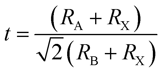 | (1) |
 | (2) |
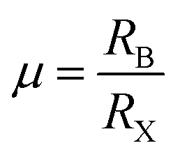
For the stable cubic structure of perovskites, the tolerance factor (t) is close to 1, however empirically it is found that a perfect 3D perovskite structure can be formed for 0.81 < t < 1.11 and 0.40 < μ < 0.90.20 When the size of A cation is too big, or the size of B cation is small, the tolerance factor t becomes >1.1, and the cubic structure of the perovskite distorts and acquires a tetragonal structure. Similarly, when the size of A-site cation is too small to fit in B cation interstices, the tolerance factor t becomes <0.8; this changes the symmetry of the perovskite cubic structure and the increase in distortion results in an orthorhombic structure.
The size of the A cation primarily influences the dimension and structure of a perovskite. A 2D perovskite structure can be formed by partially or fully replacing the smaller size A cation with larger size organic cations such as long-chain alkyl amine cations, which disrupts the 3D cubic structure and the tolerance factor lies outside the region (Fig. 1(a)).21 When the size of the A cation is too large to fit in between the space provided by the connected BX6 octahedra networks, then it causes a distortion of the 3D cubic structure, and the tolerance factor is much larger than 1. In a 2D crystal structure, the BX6 is connected with the shared X anions only in the 2D plane. The general formula for 2D layered perovskites is given by (A′)mAn−1BnX3n+1, where A′ can be divalent (m = 1) or monovalent (m = 2) cations that form a bilayer or monolayer connecting the conductor (A)n−1BnX3n+1 2D sheets, where n indicates the layer thickness or the number of layers of metal halide sheets.22 2D perovskite materials having alternate slabs enclosed with cations were first synthesized and described by S. N. Ruddlesden and P. Popper in 1957.23,24 The lateral dimension of the 2D layered perovskite is of the order of several hundred nanometers to micrometers. Generally, a long organic spacer is inserted between the layers of the metal halide octahedra sheet which in turn imposes low-dimensional optoelectronic characteristics through quantum and dielectric confinement effects of charge carriers into the inorganic layers. Structurally, the 2D structure of a perovskite is achieved by slicing the 3D cubic structure along specific crystallographic planes ((100), (111) and (110)) such that the metal–halide octahedron (inorganic layer) remains connected along only two axes, forming a layered material that is stacked via weak van der Waals interactions (Fig. 1(b)).25,26 Therefore, the X-ray diffraction (XRD) pattern of the highly oriented-layered 2D perovskite structure consists of repetitive diffraction patterns at (00n) peaks (Fig. 1(c)).27 The difference in two repetitive (00n) diffraction peaks gives the distance between two successive inorganic layers.27,28 Depending on the orientation of inorganic octahedra with the organic cation, the (100)-oriented 2D perovskite structures are further sub-divided into two crystal phases, which are Ruddlesden–Popper (RP) and Dion–Jacobson (DJ) phases. The RP phase features perovskite layers staggered by half a crystal unit cell in the two in-plane directions since each inorganic sheet is confined between bilayers of two mono-cationic bulky ammonium cations. The alkyl chains which separate the metal halide layers are connected to each other by relatively weak van der Waals forces, as shown in Fig. 1(d). On the other hand, DJ perovskites form slabs that are stacked exactly on top of each other as there is only one di-cation spacer molecule between the inorganic layers which is connected by a hydrogen bond with the metal halide layers on both the sides (Fig. 1(d)). DJ perovskite was implemented in solar cells for the first time by Kanatzidis and coworkers by using 3- or 4-(ammoniomethyl)piperidinium and methylammonium.29 In contrast to 3D perovskites where the size of the A cation should be fitted into a small portion of the crystal to fulfill the tolerance factor condition; 2D perovskites give huge structural flexibility as the distance between the inorganic sheets can vary with the length of the organic cation. Hence, 2D perovskites have widened the research field as larger and more complex functional organic cations can be incorporated in the perovskite structures which can unveil more interesting and diverse properties.
 | ||
| Fig. 1 (a) Schematic crystal structures of 3D MAPbI3, 2D (PEA)2PbI4 (PEA = phenylethylammonium), and intermediate mixed 3D–2D perovskites. Reprinted with permission from ref. 21. Copyright 2016, American Chemical Society. (b) Illustrated image of a layered 2D perovskite showing the crystal structure along different directions. Reprinted with permission from ref. 25. Copyright 2016, Wiley-VCH. (c) XRD patterns for L2PbBr4 nanoplatelets where the ligand species, L, was either octylammonium, butylammonium, or an equimolar mixture of the two. Reprinted with permission from ref. 27. Copyright 2016, American Chemical Society. (d) Schematic of Ruddlesden–Popper and Dion–Jacobson phases of 2D perovskites. Reprinted with permission from ref. 61. Copyright 2019. Elsevier Inc. | ||
3. Properties of 2D layered perovskites
The structural uniqueness of 2D perovskites results in some exceptional and interesting physical and optoelectronic properties. In general, the conduction band (CB) of the inorganic sheet is lower than that of the large organic molecules, while the valence band (VB) of the inorganic perovskite is above that of the organic layer.23 Therefore, the structure of the layered perovskite nanostructure can be considered as a multiple quantum-well (QW) electronic structure with inorganic sheets and organic molecules acting as wells and barriers, respectively. The width of the barrier and well layers can be modified by changing the size or length of the organic layer and the number of inorganic sheets between each organic layer, respectively (Fig. 2(a)).23 Different dielectric environments of the wells and barriers increase the electron–hole interaction giving rise to enhanced binding energy and reduced forbidden electron transition contributing to high luminescence efficiency (Fig. 2(b)).30,31 The restriction only along one dimension of the 2D perovskite gives the advantages of one-dimensional (1D) quantum confinement effect with higher exciton binding energy and low defect density.32 It also retains high carrier mobility along the horizontal direction due to its large lateral size.33 The quantum confinement effect of 2D perovskites along the vertical direction shifts the conduction and valence bands, which increases the overall bandgap of the material compared with the 3D perovskite. The bandgap of 2D perovskites is determined by the base 3D perovskite structure and the extra quantization energies of electrons and holes in the inorganic well.22,34 The optical bandgap of an (A′)mAn−1BnX3n+1 perovskite generally increases with decreasing layer thickness since the layer thickness or the value of n decides the degree of quantum confinement effect. In a layered perovskite, the exciton binding energy is so high (several 100 meV, more than an order of magnitude higher than its 3D counterpart) that the excitons can be stabilized even under ambient conditions making it an exciting material to be used in various applications at room temperature.35,36 In a perfect 2D system, exciton binding energy is exceptionally high by the image charge effect due to the high dielectric constant between the organic and inorganic layers (EB,2D = 4EB,3D).37 The exciton binding energy of the layered perovskite can be increased by incorporating larger organic cations since high exciton binding energy is favorable for light-emitting applications as it enhances radiative recombination giving rise to high photoluminescence (PL) emission.38 Considering an infinite series of image charges, the increase in exciton binding energy in a multi-QW 2D system can be expressed using first-order perturbation theory as given below:39,40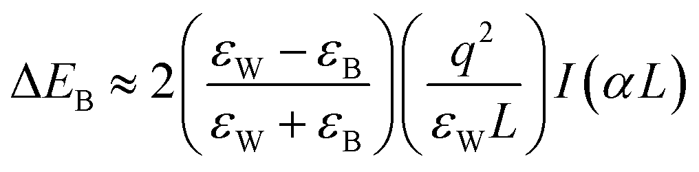 | (3) |
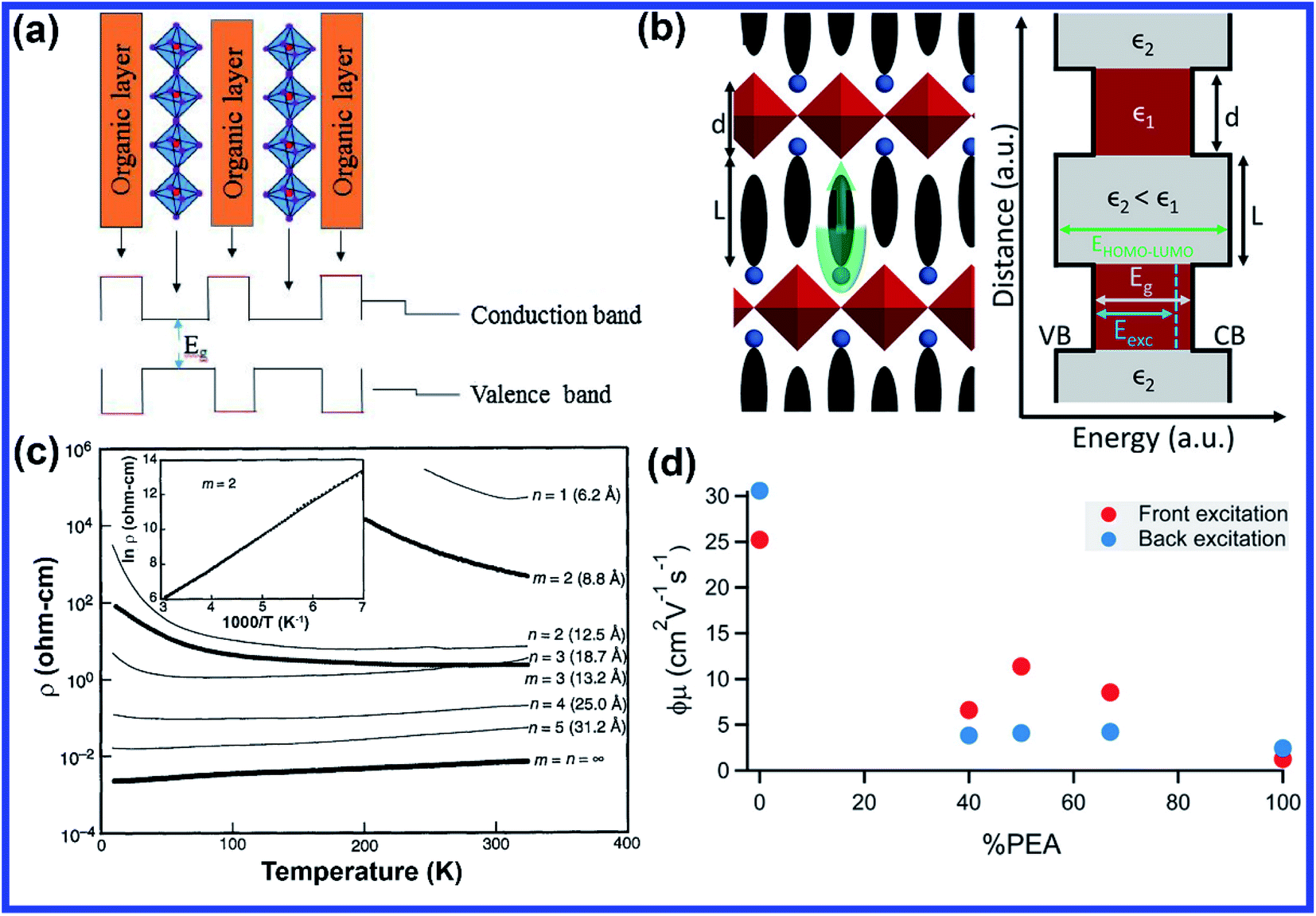 | ||
| Fig. 2 (a) Schematic representation of variation in energy levels that arise within the structure of the 2D perovskite materials. Reprinted with permission from ref. 23. Copyright 2018. Elsevier Inc. (b) Schematic of a monolayer 2D perovskite structure with alternating organic and inorganic sheets along with the corresponding multi-QW energy diagram of different dielectric environments. Reprinted with permission from ref. 30. Copyright 2018, American Chemical Society. (c) Variation of resistivity with temperature for a 2D perovskite with various thicknesses. Reprinted with permission from ref. 48. Copyright, 1995 by the American Association for the Advancement of Science. (d) Schematic showing the trend in the carrier mobility (upon decreasing n) of the (PEA)2(MA)n−1PbnI3n+1 perovskite as a function of the PEA-to-MA ratio. Reprinted with permission from ref. 21. Copyright 2016, American Chemical Society. | ||
Due to the different dielectric environments in organic and inorganic layers, conductivity and charge carrier mobility are anisotropic in nature. Conductivity and mobility are much better in the plane of the inorganic sheet layer in comparison to the out of plane organic layer of a 2D perovskite since the organic layer acts as an insulating layer between the conducting inorganic slabs. Therefore, several factors need to be improved to enhance the device performance of 2D perovskites. As the mobility of the inorganic layer is higher, if the ratio of the inorganic layer to the organic layer can be increased then it will significantly improve the mobility. Tailoring the number of inorganic layers per organic layer by adjusting the proportion of the precursor materials during synthesis is a critical tunable parameter in 2D perovskites, which not only tunes the bandgap and exciton binding energy but also adjusts the mobility and charge transfer phenomenon.30,46,47 Also, the crystallographic orientation of 2D perovskites can be made in such a way that the inorganic sheets are parallel to the charge transfer direction; this will allow a smoother charge transfer mechanism. For example, Mitzi et al. reported that (110)-oriented MASnl3 perovskite sheets separated by iodoformamidinium cations show semiconductor to metal transition as the layer number increases (Fig. 2(c)).48 Herz et al. investigated the charge transport properties and crystallographic orientation of mixed methylammonium (MA)–phenylethylammonium (PEA) lead iodide thin films as a function of the MA-to-PEA ratio.21 Interestingly, they found that effective charge-carrier mobilities are remarkably high (about 10 cm2 V−1 s−1) for intermediate PEA content (Fig. 2(d)) and monomolecular charge-carrier recombination rates first decrease with increasing PEA fraction, most likely as a result of trap passivation, but then increase significantly as excitonic effects begin to dominate for thin confined layers.21 In general, thinner 2D perovskites offer faster recombination rates, decreased carrier mobilities compared to thicker quasi 2D perovskites which promote free carrier formation and slower charge carrier recombination rates. Therefore, the properties of 2D perovskites can be modified or tuned depending on the applications or requirements.
4. The doping mechanism in 2D perovskites
Layered 2D perovskites, which were extensively used in the 1900s, have re-emerged recently as a new class of semiconducting material that offers a wide range of tunability in its photophysical properties, thus providing an excellent platform for fundamental research on doping.Due to its hybrid nature, doping study also brings new challenges and needs a deeper understanding of the crystal structure, electronic and optoelectronic properties. To determine the exact occupied position and concentration of dopants inside the material, exhaustive characterizations are needed besides the theoretical calculations. Electronic doping in inorganic semiconductors has been one of the most studied topics for decades. However, the detailed effect of doping on the photophysical properties of hybrid perovskite materials is not understood properly, and it requires a thorough study and understanding. In general, doping in perovskite materials has been explored by replacing the A, B, and X sites. Unlike 3D perovskites, layered (A′)mAn−1BnX3n+1 perovskites exhibit far greater tolerance and show a high degree of structural flexibility in accommodating a wide range of organic cations or alkali chains (Fig. 3). The distance between inorganic sheet layers or the interaction between the inorganic and organic layers of layered metal halide perovskites can be tuned by incorporating a mixture of small and large size organic cations. However, B site doping must satisfy the rule of octahedral factor (0.40 < μ < 0.90) to form BX6 inorganic octahedra. Due to the large formation energy, B-site doping is comparatively difficult. However, at the same time, the replacement of B-site Pb ion by other dopants (Fig. 3) tunes the optical, electrical and magnetic properties of perovskites since the bandgap of the perovskite is mainly comprised of p orbitals of Pb and halide ions.49 For this reason, changing or mixing the X site halogen (Cl, Br or I) ions generally tuned the bandgap of the perovskite across the entire visible region.37 Therefore, B site doping or halide exchange can primarily alter its intrinsic energy level structure and significantly manipulate its bandgap (Fig. 3). However, only Cl–Br and Br–I exchanges are attainable; but due to the significant difference in ionic radii between I− and Cl− ions, anion exchange between iodine and chlorine is not possible in halide perovskites as it involves large structural stress, which eventually destructs the perovskite crystal structure.
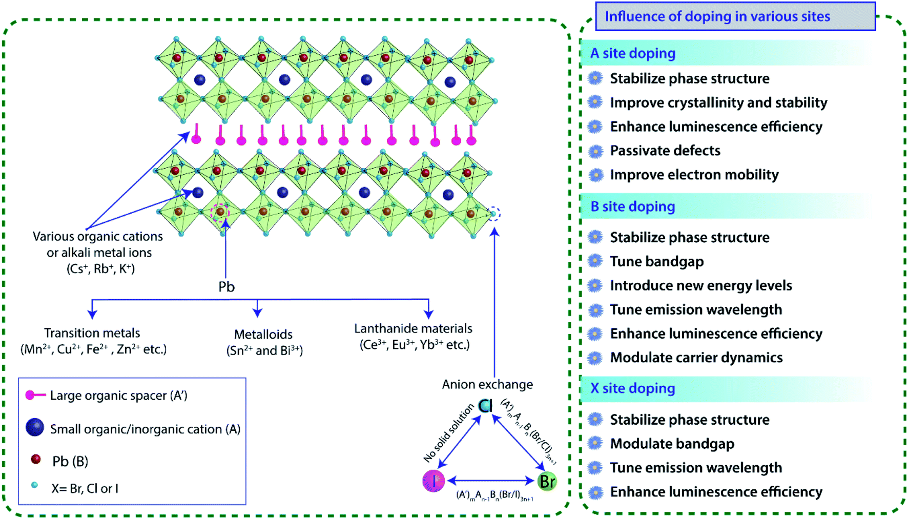 | ||
| Fig. 3 Schematic diagram of doping of various ions at different sites and their effects on 2D perovskite crystal structures. | ||
4.1 A-site doping
The layered structure in 2D perovskites gives freedom to A-site doping by inserting large cations to vary chain lengths, mixing different cations, or inserting smaller alkali cations that couldn't be doped in 3D structures. Similar to 3D perovskites, high quality and uniform 2D perovskite film is mostly synthesized using the hot-casting method. Mohite et al. originally developed the hot casting method to grow 2D (BA)2(MA)3Pb4I13 (BA = n-butylamine, C4H9NH3) films.50 The out-of-plane (BA)2MA3Pb4I13 QWs formed by hot casting are confirmed to be more beneficial for charge transfer.50 This method was further optimized to grow high-quality Cs+ doped 2D (BA)2(MA)3Pb4I13 films by introducing DMSO, which can function as a ligand to form a complex structure with the PbI2 precursor,51 Cs+ doped 2D films exhibited better crystal orientation in contrast to the pure 2D films attributed to the changed crystallization with the formation of Lewis acid–base adducts upon addition of DMSO in the DMF solution.51 Cs doping in 2D (BA)2(MA)3Pb4I13 film is also reported to effectively reduce pinholes and increase grain sizes.52 Recently, Chen et al. doped Cs+ into a 2D (BA)2(MA)3Pb3I10 (n = 3) perovskite to grow 2D layered perovskite crystals through a one-step spin-coating method.53 The best crystallinity and improved surface quality were observed with 10% Cs doping concentration. Due to the small cationic size, K+ cannot be incorporated into the 3D metal halide perovskite, but a more relaxed crystal structure of the 2D perovskite allows easy substitution of alkali cations. Bach et al. incorporated alkali (K+ and Rb+) cations into the 2D perovskite to exquisitely modulate the crystal formation.54 The tilting of the 2D metal halide perovskite is attributed to the crystal lattice distortion caused by the alkali cation doping. The grazing incident wide-angle X-ray scattering (GIWAXS) measurement showed that the addition of K+ and Rb+ cations into the 2D perovskite suppressed the 2D diffractions along the out-of-plane direction suggesting a decreased charge transfer barrier (Fig. 4(a)).54 Doping of both Rb+ and K+ leads to a prominent shift in the diffraction azimuth angle to ∼55° orientation (more vertical) relative to the substrate, which is beneficial for the charge transport across the 2D layer (Fig. 4(a)).54 Different chain lengths of alkyl organic cations significantly affect the crystal orientation, phase distribution, and properties of 2D Sn-based perovskites. Liu et al. designed 2D Sn-based Ruddlesden–Popper (RP) perovskites (A2(FA)n−1SnnI3n+1) with different alkyl chain lengths by applying alkylamine spacer cations [BA, octylamine (OA:CH3(CH2)7NH3+), and dodecylamine (DA:CH3(CH2)11NH3+)].55 They employed a simple one-step spin-coating method by dissolving an alkylamine iodide, formamidine iodide, and SnI2 with a molar ratio of 2![[thin space (1/6-em)]](https://www.rsc.org/images/entities/char_2009.gif) :3:4 in a mixed solvent of DMF and DMSO. The perovskite film containing cations with shorter alkyl chains shows highly oriented crystal grains (Fig. 4(b and c)), large crystal grains, and clear grain boundaries, whereas the increase in the chain length of the organic spacer cations gives rise to blurry grain boundaries and non-uniform morphology.55 Lin et al. synthesized a new series of 2D RP perovskites with diaminoalkane cations and investigated the effect of the methylene number (i.e., alkyl chain length) of the diaminoalkane molecules (from 3 to 8) on the formation of the 2D layered crystal structure and phase purity.56 With the increase of the alkyl chain length, the layered structure of the 2D rectangular plates became more complete along with enhanced 2D characteristic (0k0) diffractions (Fig. 4(d)).56 The replacement of BA layers between the [PbI6]4− octahedral sheets by a monolayer of DAT (1,8-diaminooctane) was accompanied by the replacement of van der Waals interactions between BA alkyl chains with a covalent –H2C–CH2– bond.56 White et al. synthesized a mixed 2D perovskite precursor solution of two butylammonium iodide isomers, namely n-butylammonium iodide (BAI) and iso-butylammonium (i-BAI) and did a detailed comparative study of the effects of both the cations as well as the dual-isomer alkylammonium cations.57n-BAI and i-BAI were mixed in different weight ratios, and the optimum was found to be 50:50 with reduced non-radiative interfacial charge recombination.57 Two inorganic sheet layers in a 2D perovskite are generally attached with each other via van der Waals interactions which are nonspecific, nondirectional, and highly distance-dependent; hence weak van der Waals interactions between interlayers cannot sufficiently stabilize the 2D layered structure.58 If by any means inorganic layers are linked by a stronger covalent bond instead of van der Waals interaction, then this should offer higher structural stability. Employing spacer cations consisting of diammoniums with two amino groups at both ends in a 2D perovskite generally eliminates van der Waals interaction and generates covalent bonds via alternately forming hydrogen bonds with the inorganic slabs without any gaps, but introduction of diammoniums requires relatively harsh processing conditions, such as use of hydroiodic acid as the additive or long-time and/or high-temperature annealing.59–62 Grätzel's group demonstrated the first example of a formamidinium (FA) containing DJ 2D perovskite material characterized by the BFAn−1PbnI3n+1 formulation through employing a novel bifunctional organic spacer (B), namely 1,4-phenylenedimethanammonium (PDMA).60 The perovskite solution was prepared by dissolving the precursor materials in a DMSO/DMF mixture and PDMA was synthesized using hydroiodic acid additive. With increasing FA amount the layer number of the DJ perovskite increases from n = 1 to n = 4. While n = 1 and n = 2 compositions adopted a preferentially parallel orientation, the n > 2 compositions displayed a preference for perpendicular orientation with respect to the substrate indicating that n ≥ 3 compositions are more effective in increasing the charge-extraction efficiency for photovoltaic applications (Fig. 4(e)).60 You et al. introduced a classic noncovalent aryl–perfluoroaryl interaction in 2D perovskites by mixing PEA and perfluorophenethylammonium (F5-PEA) in a 1:1 ratio using a simple deposition at low temperature without using any additives.58 Mixing of equimolar organic cations (PEA and F5-PEA) formed strong quadrupole–quadrupole interaction to “lock in” the interface of 2D/3D perovskite phases and stabilize the perovskite-film-based devices.58 Mixed cation 2D perovskites are also reported to be efficient for light emitting applications. Two bulky spacers phenethylammonium iodide (PEAI) and 1-naphthylmethylammonium iodide (NMAI) were used to form pure 2D (n = 1) and quasi-2D (n ≥ 2) perovskites with the formula (PEA:NMA)2Csn−1PbnI3n+1 by Shao et al.63 In comparison to single cation PEA-based perovskites, the XRD diffraction peaks of (PEA)(NMA)PbI4 and (NMA)2PbI4 films shifted to smaller 2θ values due to the increased interlayer distance caused by the larger spacer molecules of NMA.63 The formation of a cospacer perovskite [(PEA)(NMA)PbI4] was confirmed by the XRD pattern, as the calculated lattice distance (d002) of (PEA)(NMA)PbI4 (17.07 Å) was approximately half of the sum value of (PEA)2PbI4 (16.03 Å) and (NMA)2PbI4 (18.09 Å) and mixed cation film oriented from the horizontal toward the vertical direction with respect to the substrate.63 Effects of various A-site dopants and growth methods are summarized in Table 1.
:3:4 in a mixed solvent of DMF and DMSO. The perovskite film containing cations with shorter alkyl chains shows highly oriented crystal grains (Fig. 4(b and c)), large crystal grains, and clear grain boundaries, whereas the increase in the chain length of the organic spacer cations gives rise to blurry grain boundaries and non-uniform morphology.55 Lin et al. synthesized a new series of 2D RP perovskites with diaminoalkane cations and investigated the effect of the methylene number (i.e., alkyl chain length) of the diaminoalkane molecules (from 3 to 8) on the formation of the 2D layered crystal structure and phase purity.56 With the increase of the alkyl chain length, the layered structure of the 2D rectangular plates became more complete along with enhanced 2D characteristic (0k0) diffractions (Fig. 4(d)).56 The replacement of BA layers between the [PbI6]4− octahedral sheets by a monolayer of DAT (1,8-diaminooctane) was accompanied by the replacement of van der Waals interactions between BA alkyl chains with a covalent –H2C–CH2– bond.56 White et al. synthesized a mixed 2D perovskite precursor solution of two butylammonium iodide isomers, namely n-butylammonium iodide (BAI) and iso-butylammonium (i-BAI) and did a detailed comparative study of the effects of both the cations as well as the dual-isomer alkylammonium cations.57n-BAI and i-BAI were mixed in different weight ratios, and the optimum was found to be 50:50 with reduced non-radiative interfacial charge recombination.57 Two inorganic sheet layers in a 2D perovskite are generally attached with each other via van der Waals interactions which are nonspecific, nondirectional, and highly distance-dependent; hence weak van der Waals interactions between interlayers cannot sufficiently stabilize the 2D layered structure.58 If by any means inorganic layers are linked by a stronger covalent bond instead of van der Waals interaction, then this should offer higher structural stability. Employing spacer cations consisting of diammoniums with two amino groups at both ends in a 2D perovskite generally eliminates van der Waals interaction and generates covalent bonds via alternately forming hydrogen bonds with the inorganic slabs without any gaps, but introduction of diammoniums requires relatively harsh processing conditions, such as use of hydroiodic acid as the additive or long-time and/or high-temperature annealing.59–62 Grätzel's group demonstrated the first example of a formamidinium (FA) containing DJ 2D perovskite material characterized by the BFAn−1PbnI3n+1 formulation through employing a novel bifunctional organic spacer (B), namely 1,4-phenylenedimethanammonium (PDMA).60 The perovskite solution was prepared by dissolving the precursor materials in a DMSO/DMF mixture and PDMA was synthesized using hydroiodic acid additive. With increasing FA amount the layer number of the DJ perovskite increases from n = 1 to n = 4. While n = 1 and n = 2 compositions adopted a preferentially parallel orientation, the n > 2 compositions displayed a preference for perpendicular orientation with respect to the substrate indicating that n ≥ 3 compositions are more effective in increasing the charge-extraction efficiency for photovoltaic applications (Fig. 4(e)).60 You et al. introduced a classic noncovalent aryl–perfluoroaryl interaction in 2D perovskites by mixing PEA and perfluorophenethylammonium (F5-PEA) in a 1:1 ratio using a simple deposition at low temperature without using any additives.58 Mixing of equimolar organic cations (PEA and F5-PEA) formed strong quadrupole–quadrupole interaction to “lock in” the interface of 2D/3D perovskite phases and stabilize the perovskite-film-based devices.58 Mixed cation 2D perovskites are also reported to be efficient for light emitting applications. Two bulky spacers phenethylammonium iodide (PEAI) and 1-naphthylmethylammonium iodide (NMAI) were used to form pure 2D (n = 1) and quasi-2D (n ≥ 2) perovskites with the formula (PEA:NMA)2Csn−1PbnI3n+1 by Shao et al.63 In comparison to single cation PEA-based perovskites, the XRD diffraction peaks of (PEA)(NMA)PbI4 and (NMA)2PbI4 films shifted to smaller 2θ values due to the increased interlayer distance caused by the larger spacer molecules of NMA.63 The formation of a cospacer perovskite [(PEA)(NMA)PbI4] was confirmed by the XRD pattern, as the calculated lattice distance (d002) of (PEA)(NMA)PbI4 (17.07 Å) was approximately half of the sum value of (PEA)2PbI4 (16.03 Å) and (NMA)2PbI4 (18.09 Å) and mixed cation film oriented from the horizontal toward the vertical direction with respect to the substrate.63 Effects of various A-site dopants and growth methods are summarized in Table 1.
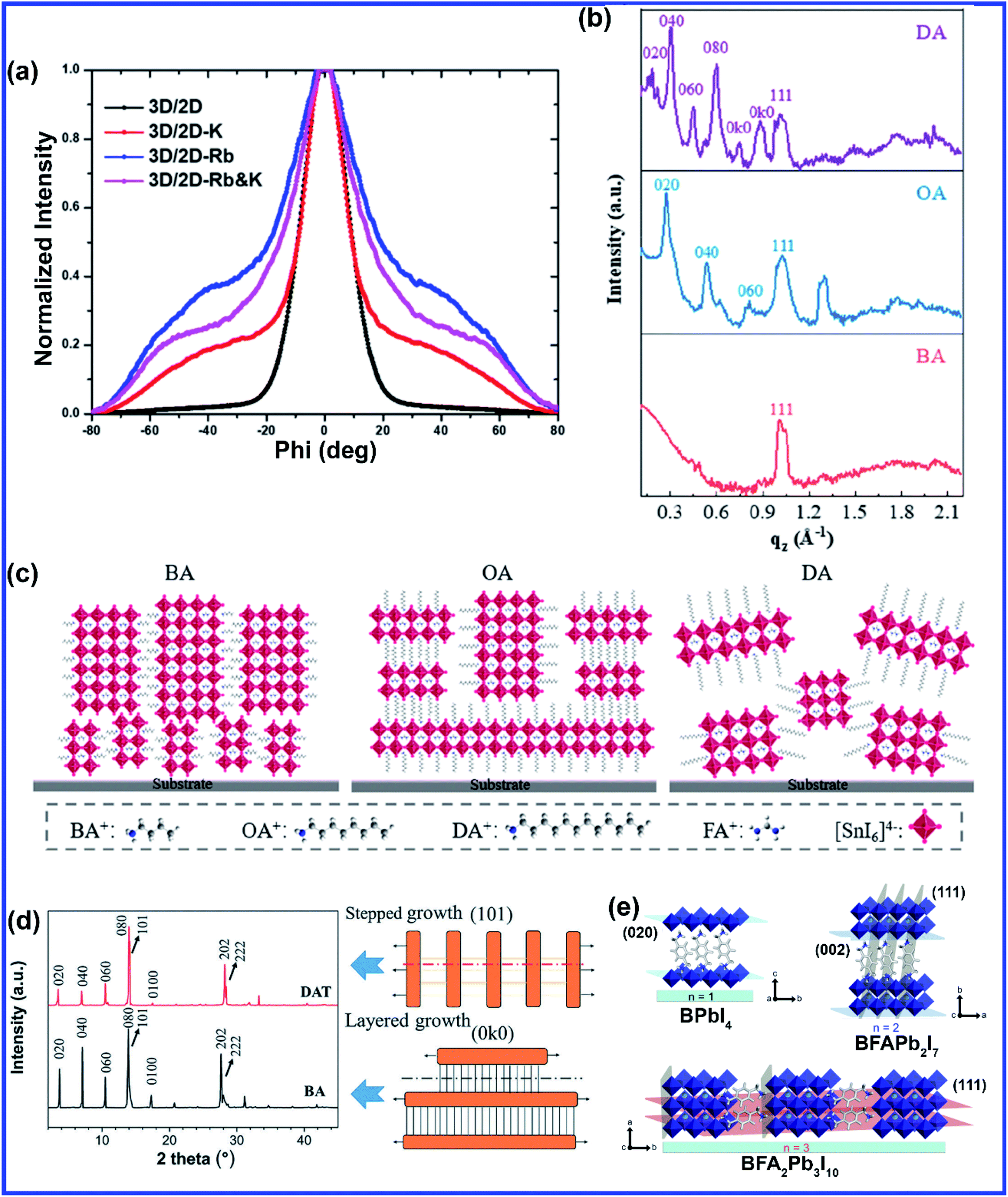 | ||
| Fig. 4 (a) Integrated GIWAX patterns azimuthally over the ring at q = 0.33 Å−1, corresponding to the (020) plane for alkali cation-doped (5% Rb+, 5% K+, and 5% Rb++ + 5% K+) 3D/2D perovskite. Reprinted with permission from ref. 54. Copyright 2020, American Chemical Society. (b) Comparison of GIWAX intensity profiles along the qz axis and (c) schematic illustration of the crystal orientation of 2D perovskite films based on BA, OA and DA. Reprinted with permission from ref. 55. Copyright 2020, American Chemical Society. (d) Comparison of the XRD patterns of DAT and BA-based perovskites along with the schematic diagram of the proposed crystal growth mechanism for the 2D halide perovskite between BA and DAT. Reprinted with permission from ref. 56 with permission from the Royal Society of Chemistry. (e) Schematic representation of the crystal structure packing of the films with different BFAn−1PbnI3n+1 perovskite compositions (n = 1, 2 and 3). Reprinted with permission from ref. 60. Copyright 2019, American Chemical Society. | ||
| 2D perovskite | Dopants | Growth method | Mechanism | Ref. |
|---|---|---|---|---|
| (BA)2(MA)3Pb4I13 | Cs+ | Hot-casting | Better crystal orientation, increased grain size of the 2D planes, improved surface quality | 51 |
| (BA)2(MA)3Pb4I13 | Cs+ | Spin-coating | Defect passivation and film morphology control | 52 |
| (BA)2(MA)3Pb3I10 | Cs+ | One-step spin coating | Best crystallinity and improved surface quality with 10% doping | 53 |
| 3D/2D hybrid layer BA2(Cs0.05FA0.79MA0.16)–Pb2(I0.83Br0.17)7 | K+ and Rb+ | Anti-solvent | Suppression of out-of-plane crystal orientation | 54 |
| A2(FA)n−1SnnI3n+1 | n-Butylamine/octylamine/dodecylamine | One step spin coating | Highly oriented crystal grains, large crystal grains and clear grain boundaries with shorter alkyl chains | 55 |
| (BA)2(MA)2Pb3I10 | Different diaminoalkane molecules | HI-assisted synthesis and spin coating method for film | The size of the 2D rectangular plates increases with increasing alkyl chain length | 56 |
| (PDMA)(FA)n−1PbnI3n+1 | Different FA concentrations | HI-assisted synthesis and spin coating method for film | Layer number of the perovskite increases from n = 1 to n = 4 with increasing FA concentrations | 60 |
| PEA2PbI4 | F5-PEA | Low-temperature precipitation without any additives | Aryl–perfluoroaryl interaction into 2D perovskites due to mixing of PEA and F5-PEA | 58 |
| PEA2PbI4 | NMAI | Simple solution processing with the addition of tetraphenylphosphonium chloride | The orientation of quasi-2D crystals gradually aligns from the horizontal toward the vertical direction with respect to the substrate | 63 |
4.2 B-site doping
Compared to A and X sites, B-site doping is found to be the most challenging due to its high formation energy, and complete substitution of Pb2+ mainly deteriorates the outstanding properties of lead halide perovskite. However, B-site doping is the most interesting as it strongly impacts the energy bandgap due to its significant contribution to the valence and conduction bands of the perovskite. Mn doping in 3D perovskite structures is extensively reported and has had great success in introducing interesting optical properties as it manifests host to dopant energy transfer. Though Mn2+ ions can be directly doped into 3D MAPbCl3/CsPbCl3 systems, the same direct strategy does not work for MAPbBr3/CsPbBr3 systems due to the higher bond strength of the Pb–Br bond than Mn–Br bonds.64 In general, the anion exchange strategy has been adopted on the Mn2+ doped CsPbCl3 systems to prepare Mn2+ doped CsPbBr3 NCs.64,65 The layered structure of 2D perovskites allows easy incorporation of Mn2+ even in Br-based perovskites. For the first time, Kundu et al. reported the simple and scalable synthesis of Mn2+-doped (C4H9NH3)2PbBr4 2D layered perovskites.66 First, the host material (C4H9NH3)2PbBr4 was synthesized following Yang's synthesis method by slow cooling of a hot solution of PbBr2 and (C4H9NH3)Br in a DMF/toluene mixture with 2–3 drops of concentrated HBr aqueous solution.66,67 Then Mn2+ impurity ions were incorporated into (C4H9NH3)2PbBr4 by simple solid-state grinding of (C4H9NH3)2PbBr4 single crystals and MnBr2 in the desired ratio, followed by an hour of annealing at 125 °C.66 These simple solid state grinding methods incorporating Mn2+ in layered Br-based perovskites worked for various organic cations but did not work for the 3D CsPbBr3 system.66 The reason for easy, facile incorporation of Mn2+ in bulk 2D systems was attributed to the inherent mechanical and electronic “softness” of constituent atoms of the 2D layered perovskites.66 Micron-sized 2D plate/disk-like Mn2+ doped (BA/OA)2PbBr4 perovskites were also fabricated utilizing a facile one-pot micro-emulsion based synthetic methodology (Fig. 5(a)).68 X-ray diffraction peaks of Mn-doped (BA/OA)2PbBr4 perovskites monotonically shifted towards higher diffraction angles with increasing MnBr2 concentration, indicating lattice contraction due to the substitution of Pb2+ ions (ionic radius = 1.33 Å) with smaller Mn2+ ions (ionic radius = 0.97 Å) as dopants.68 High-temperature annealing also influences the dopant-dependent properties, as XRD peaks of the Mn-doped sample show a shift after thermal annealing at 100 °C due to thermal diffusion of Mn ions into the host perovskite crystal.68 Note that strong electron–phonon interaction can weaken the emission intensity of 2D perovskites. Wang et al. incorporated Mn2+ in a 2D perovskite to suppress electron–phonon interaction.69 Distorted [PbI6]4− octahedra by Mn doping and the rigid benzimidazolium (BIZ) ring without branched chains in the 2D perovskite structure improved the crystallinity and rigidity of the perovskites.69 Upon Mn2+ doping, the diffraction peaks are shifted to lower diffraction angles suggesting an increase in layer distance from 13.88 Å to 13.99 Å due to the distorted and decreased size of the cavities between adjacent corner-shared octahedra as the Pb ion (ionic radius 133 pm) was substituted by the smaller-sized Mn ion (ionic radius 97 pm).69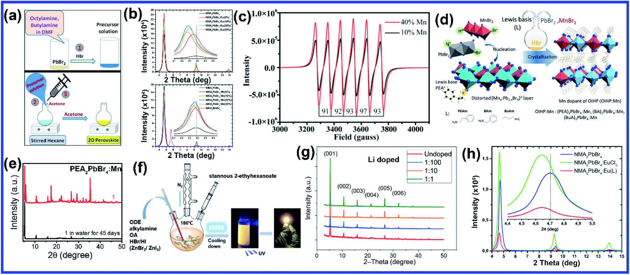 | ||
| Fig. 5 (a) Schematic of the one-pot micro-emulsion synthesis procedure of BA2PbBr4 perovskite. Reprinted with permission from ref. 68. Copyright 2019, Wiley-VCH. (b) XRD patterns of Eu and Mn doped NMA2PbBr4 perovskites. Reprinted with permission from ref. 71. Copyright 2019, Elsevier. (c) EPR spectrum of EA2PbBr4:Mn2+ perovskite. Reprinted with permission from ref. 72. Copyright 2019, American Chemical Society. (d) Schematic illustration of the synthesis procedure of pure and Mn doped 2D organic–inorganic halide perovskite through acid solution-assisted Lewis-base precipitation method and (e) comparison of the XRD patterns of fresh and water immersed Mn doped PEA2PbBr4 perovskite. Reprinted with permission from ref. 76. Copyright 2019, Wiley-VCH. (f) Schematic diagram of the synthesis of the 2D (RNH3)2SnX4 perovskite by the hot-injection method. Reprinted with permission from ref. 84. Copyright 2021, Royal Society of Chemistry. (g) XRD patterns of Li doped 2D perovskite. Reprinted with permission from ref. 87. Copyright 2020, Springer Nature. (h) Comparison of the XRD patterns of pure, Eu3+ doped and europium chelate doped NMA2PbBr4 perovskites. Reprinted with permission from ref. 88. Copyright 2021, American Chemical Society. | ||
The post-synthetic process is another efficient doping strategy. 2D Mn-doped CsPbCl3 perovskite nanoplatelets (NPLs) were prepared via a two-step synthetic method by Zheng et al.70 First, lightly doped 2D Mn:CsPbCl3 NPLs were synthesized by injecting Cs-oleate into an oleic acid and oleylamine (OAm) solution containing PbCl2 and MnCl2 at 120 °C.70 Then the heavily doped Mn:CsPbCl3 NPLs were prepared by transferring the solution into an autoclave under solvothermal conditions at 200 °C for 2–5 h.70 Post solvothermal treatment there was an increase in the size of the NPLs, which were lying flat on the TEM grid with a few lying perpendicular to the TEM grid, suggesting the formation of larger 2D NPLs as a result of oriented attachment of the small 2D NPLs under solvothermal conditions.70 Surprisingly, instead of the usual shifting of the diffraction peaks towards higher angles, two new XRD peaks at 30.9° and 35.3° gradually appeared for higher Mn concentrations and longer solvothermal treatment, which were identified with the (122) and (200) lattice planes of orthorhombic CsMnCl3 and cubic CsMnCl3, respectively.70 The EPR spectra of the 2D Mn:CsPbCl3 NPLs exhibited a continuously broadened dipolar background with weakened hyperfine peaks with increasing solvothermal treatment time, indicating the presence of short-range Mn–Mn interactions, which occurred due to higher Mn doping concentrations and longer solvothermal growth time.70 The application of monolayered 2D perovskites is strongly limited due to the presence of trap-assisted recombination. Inorganic doping (Eu3+ and Mn2+) in single-layered 2D (NMA)2PbX4 perovskites proved to overcome the fast exciton quenching.71 Undoped NMA2PbBr4 films were deposited using a spin-coating method by dissolving the organic salt (NMA)Br and the inorganic precursor PbBr2 in DMF solutions. For the doped film, MnBr2 and EuCl3 were added to the spin-coating solution.71 Post doping, relative intensities of various host diffraction peaks changed due to either a change in the scattering factors after doping or a slight difference in the preferential orientation induced by the presence of the dopant.71 Unlike previous cases, a clear shift in the diffraction peak towards lower angles is observed in the Mn doping system though the change was less compared to the Eu-doped system as the size of Eu3+ ion is bigger than that of Mn2+ ion (Fig. 5(b)).71 The shift was attributed to the fact that the introduction of the doping element might force a different coordination of the NMA+ cation, creating disorder in the organic layer and ultimately leading to widening of the interplanar distance.71 Zhang et al. also synthesized Mn2+ doped 2D distorted single-layered EA2PbBr4 crystals.72 In comparison to other single-layered perovskites, the lead bromide framework in EA2PbBr4 was highly twisted, resulting from the dual interaction including hydrogen bonding and electrostatic interaction between ammonium and [PbBr6]4− octahedra.72 EPR spectra (Fig. 5(c)) of Mn2+ doped EA2PbBr4 showed hyperfine splitting without significant interference, which ruled out the existence of Mn2+ with a different coordination environment and suggested weak Mn–Mn exchange interaction. This indicated homogeneous Mn2+ doping in the system.72 The 2D single-layer feature of EA2PbBr4 played a vital role in promoting the easy substitution process because all the Pb2+ sites were exposed, and Mn2+ could easily enter in place of Pb2+ during the synthesis procedure.72 Nag et al. reported Mn doping in centimeter-sized 2D layered BA2PbBr4 single crystals following a one-pot solution synthesis process through slow cooling of the aqueous hydrobromic acid solution of lead oxide, manganese bromide, and butylammonium bromide.73 However, Mn doping efficiency was low in the 2D single crystal (1.08% Mn compared to Pb), resulting in no noticeable effect on the crystal structure of the layered BA2PbBr4 perovskite.73 The sharp six-line hyperfine splitting patterns in EPR spectra and ∼9.6 mT hyperfine splitting energy confirmed the presence of isolated Mn2+ ions as well as Mn2+ ions in the octahedral coordination environment, respectively.73 A Mn doped 2D layered perovskite has shown excellent storage and water stability which is one of the major limitations of 3D perovskites in practical applications. Mn-doped 2D PEA2PbBr4 perovskite nanosheets were synthesized using a very convenient hot injection method with higher stability than the Mn doped CsPbCl3 perovskite.74 Several grams of doped perovskite powder with bright orange emission were obtained by scaling up the precursor dosage using the hot injection method. The crystal structure of the Mn-doped 2D PEA2PbBr4 perovskite was also well preserved after storage for over 300 days.74 Gram-scale production of the Mn-doped 2D (C8H17NH2)2PbBr4 perovskite with a solid yield of 1.35 g products out of 3 mL solvent was recently reported by Li et al. using a one-step acid solution-assisted method.75 The synthesis method is extremely simple and cost-efficient as one only needs to mix the raw materials lead monoxide, hydrobromic acid, MnBr2, and octylamine, in an open-air atmosphere in a glass bottle and then put it in a vacuum oven at 100 °C for 3 h to dry.75 The XRD peaks in Mn-doped perovskites shifted to lower angles with increasing Mn concentration in (C8H17NH2)2PbBr4 due to the increase in disorder between the organic layer, similar to Mn-doped (NMA)2PbX4 and (BIZ)2PbI4 perovskites.69,71,75 The crystal structure and optical properties of the Mn-doped (C8H17NH2)2PbBr4 perovskite were unchanged for 90 days under ambient conditions, implying its higher ambient stability.75 Various pure and Mn-doped 2D organic–inorganic (OI) halide perovskites ((PEA)2PbBr4, (BAm)2PbBr4, and (BA)2PbBr4) (BAm = benzylamine) were synthesized through acid solution-assisted Lewis-base precipitation method, which improved the stability of the system compared to the Mn doped perovskites synthesized using other conventional methods (Fig. 5(d)).76 Mn doping shifted the diffraction peaks towards higher angles which confirmed the fact that the Mn2+ ion preferably occupied the position of Pb2+ without accumulating in the interstices during perovskite NC formation.76 Compared to other organic cations, Mn-doped 2D PEA-based perovskite NCs showed the best tolerance to water corrosion due to the hydrophobic organic layer and dopant ion-controlled lattice structure.76 Even after immersing the Mn-doped perovskite material in water for 45 days, the crystal structure and NPL morphology were retained (Fig. 5(e)).76 The average contact angles of the hydrophilicity for glass and Mn doped PEA based perovskite NC films were 22.8° and 14.8°, respectively and the contact angle of water on glass slowly decreased whereas that on Mn doped films was unchanged.76 The hydrophobic PEA+ molecules may reduce water adsorption energy and prevent water ingression into the sublattice of the layered structure.76 Also, the substitution of Pb2+ ions with smaller Mn2+ ions contracted the lattice cell and thus enhanced the formation energy of the perovskite lattice cell, which increased the energy barrier for water diffusion into the inner structure.76 As a result, Mn-doped film showed excellent water-repelling ability. Water stable, large area Mn-doped PEA2PbI4 perovskite and polymer composite film was fabricated using an in situ doctor blade method.77 Polyvinylidene fluoride (PVDF), with its excellent hydrophobicity, thermal stability, and film-forming property, is an ideal choice for protecting 2D perovskites from harsh environments.77 To deposit polymer composite Mn-doped perovskite film, first, a uniform mixture of perovskite and PVDF polymer was coated onto a glass substrate via the doctor blade method, then the substrate was transferred to an oven and dried at 50 °C for two hours, and Mn-doped 2D perovskites were in situ formed in the polymer matrix.77 The dark yellow color composite film was peeled off from the substrate for characterization. The composite film exhibited excellent water soaking stability as the crystal structure and morphology of the composite film only slightly changed after soaking it in hot water for 450 h.77 The water contact angle of the water-soaked film increased from 86.09° to 98.79° indicating that the surface perovskite was dissolved to leave the hydrophobic PVDF polymer.77 Thus, the water stability of PEA-based 2D perovskites could be further enhanced using polymer composite film showing its great potential to be used under harsh conditions. Recently, a simple room-temperature synthesis method was reported for synthesizing Mn2+ ion-doped 2D (PEA)2PbBr4 perovskite NCs.78 For the synthesis, PEABr, PbBr2 and MnBr2 were dissolved in a mixture of 2.5 mL of DMF and 8 mL of n-octylamine under stirring at room temperature to form a perovskite precursor solution.78 Then, 30 mL of the prepared precursor solution was quickly injected into 15 mL of toluene under vigorous stirring, after which Mn2+ ion doped (PEA)2PbBr4 NCs were formed.78 Along with an obvious shift to a larger angle, some new periodic diffraction peaks were observed upon increasing the Mn2+ ion doping ratio due to a split from adjacent diffraction peaks of PEA2PbBr4 as a result of structural distortion of the host.78 Mostly Mn is doped in PEA-based perovskite nanostructures, but recently Fu et al. reported the first Mn2+ alloyed 2D (PEA)2PbBr4 perovskite solid thin film using a one-step spin-coating method.79 Separately, two solutions of pure (PEA)2PbBr4 and (PEA)2MnBr4 solutions were prepared and then they were mixed in different ratios to obtain the Mn incorporated 2D perovskite.79 The final solution was then spin-coated onto the substrate via a one-step spin-coating process at 3000 rpm for 60 s and annealed at 70 °C for 15 min.79 A series of new XRD peaks corresponding to (PEA)2MnBr4 were observed when the ratio of (PEA)2PbBr4 and (PEA)2MnBr4 solutions went beyond 1:4, but the (001) peak of doped perovskite was unchanged, indicating that the substitution of Pb2+ by Mn2+ in the 2D perovskite Mn:(PEA)2PbBr4 QWs was saturated.79
Sn-based 2D perovskites have better stability compared to their 3D counterpart, and even 2D (PEA)2SnI4 and (C18H35NH3)2SnBr4 thin films showed superior PL properties compared to CH3NH3SnI3 perovskites.80–82 Deng et al., for the first time, synthesized highly emissive 2D tin halide (OCTAm)2SnX4 perovskites in an aqueous solution with a PL QY near unity and high stability in the air without using toxic and expensive tri-n-octylphosphine (TOP) during the synthesis, which earlier limited large-scale application of 2D Sn-based perovskites.83 Later, in a pioneering work, their group reported 2D (RNH3)2SnX4 perovskites with high luminescence emission from yellow to red by the traditional hot injection method and thoroughly discussed the effects of A-site organic cation substitution and Zn2+ doping on their structural and optical properties and stability.84 For the synthesis, oleic acid (OA), alkylamine, and hydrobromic acid (HBr) were dissolved in octadecene (ODE) to form a RNH3+-halide-precursor solution, and the organic amine was partially protonated to RNH3+ through acidification. After that, the luminescent 2D (RNH3)2SnBr4 perovskites were precipitated as soon as the stannous 2-ethylhexanoate was injected at elevated temperatures (Fig. 5(f)).84 Zn2+-doped (RNH3)2SnX4 perovskite shifted the diffraction peak towards higher angles without introducing any new peak indicating that the zinc doping did not change the crystallinity of the perovskites but only contracted the lattice. Zn2+ doping also improved the film morphology with a uniform round sheet of average size ∼690 nm.84 A Bi3+ doped 2D PEA2SnBr4 perovskite single crystal was also synthesized by the cooling-induced crystallization method.85 Bi3+ doping retained the layered feature of PEA2SnBr4, but changed the crystal color from yellow to black. Due to the similar ionic radii of Sn2+ and Bi3+ cations, the XRD diffraction peaks did not show any shift with increasing Bi3+ doping concentrations but the relative intensity of the peaks changed.85 Lin et al. reported the first series of heterovalent-doped 2D RPs via Bi3+ doping for (BA)2(MA)n−1PbnI3n+1.86 Similar to the earlier case, Bi3+ doping did not significantly impact the crystal structures as the average Bi–I bond length in the BiI63− octahedron (3.07 Å) is very close to the Pb–I bond length in (BA)2(MA)n−1PbnI3n+1 crystals (3.18 Å for n = 1, 3.16 Å for n = 2, 3.14 Å for n = 3).86 Dang et al. synthesized Li doped (PEA)2PbBr4 perovskite crystals using a solution-processing method.87 The diffraction peaks did not shift with Li doping except a slight decrease in the intensity ratio of the (020) peak at 15.4° and the (003) peak at 15.9° from undoped to the highest 1:1 Li-(PEA)2PbBr4 crystals (Fig. 5(g)).87 This confirmed that there was no significant lattice distortion with Li doping due to the small ionic size of Li-ion. Lanthanide doping in 3D CsPbX3 perovskites is well explored, but lanthanide sensitization within the 2D perovskite framework has been scarcely investigated. Recently, Petrozza et al. studied the doping of NMA2PbBr4 layered perovskites with Eu3+ and Eu3+ tetrakis β-diketonate complex.88 First, the undoped NMA2PbBr4 films were synthesized by spin-coating of DMF solutions of stoichiometric amounts of the precursors (NMA)Br and PbBr2, then 10 mol% Eu3+ doping of NMA2PbBr4:Eu was achieved by adding EuCl3 to the perovskite spin-coating solution.88 The europium chelate doping was achieved by initially synthesizing the tetrakis β-diketonate complex Eu(tta)4P(Ph)4 [Eu(L)], then the prepared complex was added to the spin coating solution to form the doped system NMA2PbBr4:Eu(L).88 In both cases, the XRD diffraction peaks shifted towards smaller angles indicating increase in interplanar spacing, which was explained by partial incorporation of chlorine in NMA2PbBr4:Eu and lattice expansion for NMA2PbBr4:Eu(L) due to the formation of an intercalation compound. The diffraction peak intensity decreased in NMA2PbBr4:Eu(L), indicating the reduction in crystallinity due to the introduction of the bulky Eu complex (Fig. 5(h)).88 Ytterbium (Yb3+) and erbium (Er3+) are very popular lanthanide-based quantum cutting materials which can be sensitized by CsPbX3 perovskite to achieve high PL QY approaching ∼200%.89 For the Yb3+-doped CsPbCl3 NCs, the absorption onset corresponding to the host material (420 nm, 2.95 eV) is more than twice the Yb3+ emission energy (992 nm, 1.25 eV).89,90 Therefore, the quantum cutting phenomenon can occur where one absorbed photon of energy ≥2.95 eV can yield two emitted photons each of energy 1.25 eV; thus PL QY can reach close to 200%.89 2D nanosheet (NS) structures with CsPbX3 or MAPbX3 are composed of layers of corner-sharing PbX6 octahedra, with the capping ligand around the NS, leading to the confinement of electrons giving rise to discrete energy levels.37 Miyasaka et al. doped Yb3+ in quasi 2D CsPbCl3 films using a multi-step solution process.91 The undoped CsPbCl3 film deposition with only PbCl2 and DMSO formed a film with an amorphous feature. However, the Yb3+/Pb2+ chloride film showed strong diffraction peaks appearing periodically at 20.1° and 40.4°, assigned to (002) and (004) planes, respectively, which signified a layered perovskite structure as Yb3+ ions strongly interact with [PbCl6]4− in DMSO, thus promoting the formation of highly orientated film composed of [PbCl6]4− based low-dimensional clusters.91 They further spin coated CsCl methanol solution onto the PbCl2 film and heated at 250 °C for 5 min to convert the low-dimensional [PbCl6]4− cluster with the edge- or face-sharing structure into corner-sharing CsPbCl3 perovskites.91 After this process, various diffraction peaks corresponding to (100), (110), (111), (200), (210), and (211) crystal planes of the cubic-phase of CsPbCl3, respectively, were observed in the undoped film.91 These peaks were retained in the Yb doped layered structure along with the periodic (002) and (004) peaks, which were slightly shifted to lower angles than the earlier case confirming an increase in the interlayer distance.91 This resulted in a quasi-2D perovskite arrangement intercalating Yb3+ ions between [PbCl6]4− cluster layers which is strongly dependent on the Yb-ion concentration.91 In a recent study, we demonstrated Ce3+ and Tb3+ doping at high concentrations in 2D MAPbBr3 NSs using a solvothermal method.92 The Ce and Tb doping using the solvothermal method enabled us to tune the thickness of the 2D perovskite NS from ten layers (10L) to bilayers (2L) with increasing doping concentrations from 0 to 70 mol%.92 However, actual doping concentrations were quite low compared to the calculated one. The presence of a large amount of dopant molecules in the high pressure and high-temperature environment inside the autoclave increased the reactivity of the ligands and stimulated the exfoliation of the inorganic sheet layer, promoting a thinner NS.92 The substitution of Pb2+ by Ce3+/Tb3+ resulted in (002l) characteristic 2D diffraction peaks at low angles, which were absent in the undoped system thus confirming the formation of a pure 2D structure.92 The detailed information regarding various B-site doping strategies discussed above has been summarized in Table 2 for a better understanding.
| 2D perovskite | Dopants | Growth method | Mechanism | Ref. |
|---|---|---|---|---|
| (C4H9NH3)2PbBr4 | Mn2+ | Solid-state grinding of single crystals of (C4H9NH3)2PbBr4 and MnBr2 in the desired ratio followed by 1 h of annealing at 125 °C | Enhanced energy transfer efficiency from the strongly bound excitons of the host material to the d electrons of Mn2+ ions | 66 |
| (BA/OA)2PbBr4 | Mn2+ | One pot micro-emulsion-based synthesis | Lattice contraction with increasing doping concentration | 68 |
| (Benzimidazolium)2PbI4 | Mn2+ | Bulk solution by mixing the precursors | Suppression of exciton–phonon interaction due to improved crystallinity and rigidity of the perovskites | 69 |
| NMA2PbBr4 | Eu3+ and Mn2+ | Bulk solution by mixing the precursors | Widening of the interplanar distance due to the different coordination of the NMA+ cation with doping | 71 |
| EA2PbBr4 | Mn2+ | Antisolvent precipitation | Efficient exciton trapping by defects created by dopants and small activation energy (∼9.8 meV) between the defect states and Mn2+ d states | 72 |
| Centimeter sized BA2PbBr4 single crystal | Mn2+ | One-pot solution synthesis process through slow cooling of the aqueous hydrobromic acid solution | Low Mn doping efficiency (1.08%) in the 2D single crystal | 73 |
| PEA2PbBr4 | Mn2+ | Hot injection method | Excellent storage (over 300 days) and water stability | 74 |
| (C8H17NH2)2PbBr4 | Mn2+ | One-step acid solution-assisted synthesis | Gram scale production, good ambient stability, shift in the diffraction peak to the lower angles with increasing Mn concentration due to increased disorder between the organic layers | 75 |
| (PEA)2PbBr4, (BAm)2PbBr4, and (BA)2PbBr4 | Mn2+ | Acid solution-assisted Lewis-base precipitation method | Best tolerance to water corrosion (stable up to 45 days in water) in Mn-doped (PEA)2PbBr4 due to the hydrophobic organic layer and dopant ion-controlled lattice structure | 76 |
| PEA2PbI4 and PVDF polymer composite film | Mn2+ | In situ doctor blade method | Stable in hot water for 450 h due to increased water contact angle from 86.09° to 98.79° | 77 |
| (RNH3)2SnX4 | Zn2+ | Hot injection method | Improved film morphology | 84 |
| PEA2SnBr4 single crystal | Bi3+ | Cooling-induced crystallization | Crystal color changed from yellow to black and no shift in diffraction peak | 85 |
| (PEA)2PbBr4 crystal | Li | Solution process method | No significant lattice distortion and can work as a versatile scintillator in wide-range energy radiation detection | 87 |
| NMA2PbBr4 | Eu3+ and Eu3+ tetrakis β-diketonate complex (Eu(L)) | Simple solution processed by mixing the precursors in DMF | Shift in diffraction peaks towards smaller angles indicating increase in interplanar spacing and reduction in crystallinity with Eu(L) doping | 88 |
4.3 X-site doping
One of the most significant advantages of halide perovskites is that the emission bandgap of halide perovskites can be easily tuned from the UV to the NIR region by halide substitution in contrast to conventional semiconductors where the bandgap can only be altered through alloying or changing the dimensionality. Cruciani et al. first demonstrated the effect of chloride ions on ethylenediammonium lead iodide (EDPbI4) perovskite.93 For the synthesis, ED2+ and Pb2+ precursors were mixed in an equivalent ratio in HI solution which then resulted in two distinct phases (yellow cubes of EDPbI4 and pale-yellow flakes of unreacted organic salt) due to the insolubility of ethylenediamine dihydroiodide in HI. After adding a few drops of HCl to the solution, the color of the solution changed from yellow to orange suggesting the change in the crystal structure and formation of a new phase of [(ED)2PbI4]Cl2 crystals. The existence of equidistant (002l) diffraction peaks confirmed the vertical orientation of the crystal along the c-axis. The color of the [(ED)2PbI4]Cl2 crystals changed from orange to dark brown after some time which again reverted to reddish orange after keeping the sample in the oven at 100 °C for four days.93 However, the color change did not transform the crystal structure. Interestingly, halide substitution did not occur in this system; instead, the isolated Cl ions were accommodated in the ab-plane halfway between the inorganic sheets resulting in the formation of undistorted PbI42− layers by decreasing the ED cation interactions with PbI42− sheets through reducing the number of N–H⋯I hydrogen bonds as well as lengthening the H-bond distances (Fig. 6(a)).93 Though halide substitution of Cl in place of Br in a quasi-2D perovskite structure facilitates thinner and smoother film, it reduces the stability due to the ion migration behavior.94 Thus, stability is still a major concern for mixed halide perovskites which limits its use in optoelectronic devices. KI doping in (C6H9C2H4NH3)2PbBr4 (CHPB) perovskite improves the thermodynamic stability of mixed halide perovskite lattices until 60 mol% of iodine concentrations.95 At low iodine concentrations, the entropy of the system was increased and stabilized Br–I mixing in the 2D perovskite, but at high concentrations, entropy is not sufficient to stabilize the mixed-phase; thus, phase-separated single anion perovskite phases were favored.95 With increase in the doping concentration of KI from 5 vol% to 60 vol%, the interplanar spacing increased from 1.711 to 1.734 nm due to the substitution of the smaller sized Br ion (∼114 pm) by the larger sized I ion (∼133 pm). Strong diffraction peaks corresponding to (002) planes were observed even in highly KI doped crystals confirming highly c-axis-oriented growth perpendicular to the substrate (Fig. 6(b)). A diffraction peak corresponding to KBr was observed for 40 vol% doping concentrations suggesting the formation of KBr during the reaction of KI with CHPB, and KBr occupied the interstitial site within the crystal structure of perovskite below 40 vol% KI, as shown in Fig. 6(b and c). The presence of KBr was also observed on top of heavily doped mixed perovskite film micro-crystallites.95 Post-synthesis treatment with FABr on quasi-2D FA4Pb5I16 perovskite film resulted in much-improved film quality, crystallinity, and crystal orientation.96 GABr treatment also facilitated the formation of a shiny and smooth surface of the 2D GA2MA4Pb5I16 film with tuning the perovskite recrystallization and improving the crystallinity which then induce the rearrangement of the 2D perovskite phase distribution.97 With increasing GABr concentrations, the crystal grain size increased from 210 nm to 500 nm due to secondary crystallization. Johnson et al. examined the interlayer energy transfer of a series of n = 1 DJ 2D (1,5-NDA)PbX4 (NDA = naphthalene diammonium) mixed halide perovskites by varying the halide composition from pure Br to pure I.98 The mixed halide compositions were prepared by combining the bromide and iodide perovskite stock solutions together at their nominal ratios and the mixed halide solution was then spun coated on cleaned quartz substrates at 4000 rpm for 60 s, followed by annealing at 140 °C for 20 min to prepare the thin film.98 Duo et al. fabricated a vertical heterostructure of (BA)2PbBr4–(BA)2(MA)2Pb3I10 perovskites through mechanical exfoliation to study the role of organic cations in inhibiting anionic interdiffusion across heterojunctions.99 For the same thickness of the perovskite layer, iodine ion diffusion is substantially higher in (BA)2(MA)2Pb3I10 (n = 3) compared to bromide ions due to the larger number of organic barriers in the (BA)2PbBr4 (n = 1) perovskite. Also, it was found that anionic migration is faster for a higher n number in (BA)2PbBr4–(BA)2(MA)n−1PbnI3n+1 vertical heterostructures, and bulky and rigid thiophene-based conjugated organic cations are much more effective stabilizers and inhibitors of halide interdiffusion as compared to short aliphatic chains.99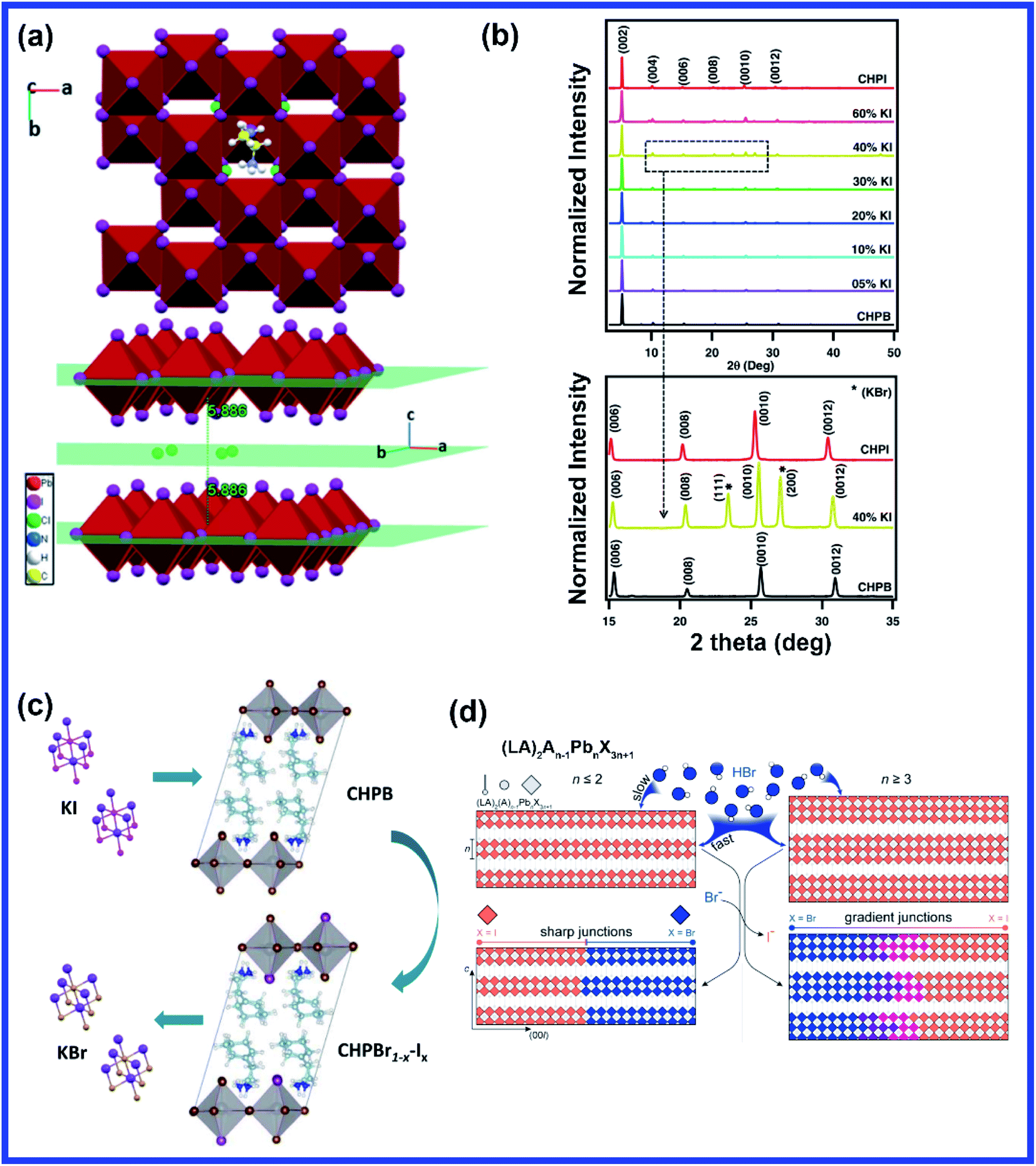 | ||
| Fig. 6 (a) Schematic diagram of EDPbI4 crystal and accommodation of chloride ions in the ab-plane between the inorganic sheet layers. Reprinted with permission from ref. 93. Copyright 2020, Royal Society of Chemistry. (b) XRD spectra of the mixed halide 2D perovskite with different vol% of KI and (c) schematic presentation of the formation of the mixed halide perovskite with the inclusion of KI and the byproduct. Reprinted with permission from ref. 95. Copyright 2020, American Chemical Society. (d) Schematic illustration depicting the different outcomes of vapor–solid anion exchange in lead iodide perovskites using HBr vapor depending on the layer thickness. Reprinted with permission from ref. 101. Copyright 2021, American Chemical Society. | ||
Vertical heterostructures can be easily prepared using various halide perovskites by mechanical stacking or direct layer by layer growth. However, the growth of lateral heterostructures with layered perovskite materials is very challenging due to ionic diffusion and instability under aggressive synthesis conditions at high temperature. Compared to 3D perovskites where ionic diffusion is more vulnerable, 2D layered perovskites have better environmental flexibility due to their inherently soft crystal lattice which allows greater tolerance to lattice mismatch. Dou et al. first reported an effective solution-processed strategy to inhibit in-plane halide diffusion in single layer (2T)2PbI4–(2T)2PbBr4 (2T+ = bi-thiophenylethylammonium) and (BA)2PbI4–(BA)2PbBr4 perovskite heterostructures.100 First, the diluted perovskite solution was added onto the SiO2 substrate placed at the bottom of a 4 mL glass vial which was then transferred to a capped secondary glass vial (20 mL) containing 3 mL of chlorobenzene onto a 70 °C hot plate. Chlorobenzene inside the secondary vial acted as an antisolvent, slowing down the solvent evaporation from the substrate and facilitating the formation of large 2D halide perovskite NSs. To form the heterostructure, first (2T)2PbBr4 NS was deposited since it has lower solubility in quaternary solvents. Then, the (2T)2PbI4 NS was grown on top of it under milder growth conditions by reducing the hot plate temperature to 50 °C to avoid any damage to the first layer. Inter-diffusion of Br and I ions, which is very prominent in 3D perovskites, was inhibited using large 2T+ conjugated ligands. The interface of the (2T)2PbI4–(2T)2PbBr4 heterojunction was found to remain more stable and well-ordered even at elevated temperatures compared to the (BA)2PbI4–(BA)2PbBr4 heterojunction due to the lower interfacial disorder and lower halide vacancy concentration.100 Following the same growth strategy, various lateral heterostructures of different halides, metal cations, and organic ligands could also be prepared.100 Recently, Jin et al. synthesized lateral heterostructures of several (LA)2(A)n−1PbnI3n+1 perovskites (where LA = FA, PEA, MA etc.) via vapor–solid anion exchange of single-crystal RP perovskite microplates with HBr vapor.101 The halide exchange was performed by exposing the RP microplates to a controlled flow of HBr vapor at room temperature in a gas flow reactor for specified periods of time.101 Since the size of the H+ cation is too small to enter in place of A-cations, no redox chemistry was involved in the reaction. It was found out that the anion exchange behavior in 2D perovskites is layer number dependent since anion exchange kinetics is substantially faster in the lateral direction along the basal planes of the Pb–X networks than in the vertical out-of-plane direction for n ≥ 3 compared to single and bilayer perovskite heterostructures (Fig. 6(d)).101 Thus, a sharp lateral heterostructure was formed for n = 1 and 2, while a diffuse gradient of color was observed for multilayer perovskites.101 Details of various X site-doped 2D perovskites in terms of synthesis methods and structural properties are summarized below in Table 3.
| 2D perovskite | Dopants | Growth method | Remarks | Ref. |
|---|---|---|---|---|
| EDPbI4 | Cl | Acid-assisted synthesis | Halide substitution didn't occur, but isolated Cl ions accommodated in the ab-plane and crystal oriented along the c-axis | 93 |
| (C6H9C2H4NH3)2PbBr4 | KI | Sol–gel method | Improved thermodynamic stability at low doping concentration due to increased entropy and highly c-axis-oriented growth | 95 |
| Quasi-2D FA4Pb5I16 | FABr | Post-synthesis treatment with FABr | Improved film quality, crystallinity and crystal orientation | 96 |
| GA2MA4Pb5I16 film | GABr | Spin coating of a mixed solution of MAPbI3 and GA2PbI4 and treated with GABr | Improved crystallinity, shiny and smooth surface and increment in crystal grain size due to secondary crystallization with increasing GABr concentration | 97 |
| (1,5-NDA)PbX4 | Br and I | Solution processed by mixing the pure halide perovskites | Interlayer energy transfer | 98 |
| (LA)2(A)n−1PbnI3n+1 | HBr | Vapor–solid anion exchange | Anion exchange behavior in 2D perovskites is layer number dependent and the sharp lateral heterostructure formed for n = 1 and 2 while a diffuse, gradient of color for multilayer perovskites | 101 |
4.4 Molecular doping
Molecular doping is proved to be an effective way to improve the electronic properties of 3D perovskite devices which in turn boost the device performance. However, it is not explored much, and the mechanism of molecular doping is not understood properly. Introducing an organic charge-transfer complex in the layered perovskite by combining charge-donating and charge-accepting molecules can include ambipolar charge transport, photoconductivity, etc. The combination of pyrene-butylammonium (PyrC4) as a donor molecule with the strong acceptor molecules tetracyanoquinodimethane (TCNQ) and tetracyanobenzene (TCNB) forms a self-assembled charge transfer layer in the organic layer of 2D perovskites with significant effect on the optical properties.102,103 Later, the same group showed that the introduction of charge-transfer complexes between the inorganic layers of 2D perovskites led to long-lived hole conduction in the inorganic octahedral layer after charge separation from the organic charge-transfer complex, but the efficiency of charge transfer was relatively low.104 Stupp et al. included tetrachloro-1,2-benzoquinone (TCBQ) into the precursor solution of A2PbX4 2D perovskite with naphthalene-based cations, which enabled the tuning of the 1s exciton binding energy of the materials and increased the electrostatic screening of the exciton, and in turn lowered its binding energy relative to the undoped perovskite.105 Liu et al. developed FA derivative-based spacers for 2D RP perovskites and studied the effect of fluorine in organic spacers.106 They have synthesized perovskite films of benzamidine (PhFA) [(PhFA)2MAn−1PbnI3n+1−xClx (n = 5)] and para-fluorobenzamidine (p-FPhFA) [(p-FPhFA)2MAn−1PbnI3n+1−xClx (n = 5)] using a one-step spin-coating method.106 The perovskite solution was prepared by mixing all the precursors (p-FPhFA or PhFA, MAI, and PbI2) in a particular stoichiometric ratio in DMF. The diffraction peak intensity ratio of (202)/(111) increases from 0.32 to 0.48 for the p-FPhFA film compared to the PhFA film, indicating more inclination towards vertical growth on the substrate, thus facilitating efficient charge transport in the device.106 However, parallel and vertical growth slabs coexist in the PhFA layered perovskite crystal film, which could block efficient charge transport.106 Hence, molecular doping in layered perovskites is still underexplored, and it should be investigated further to unveil the detailed mechanism and its effect on electronic properties.5. Effect of doping on the properties of 2D perovskites
5.1 A-site doping induced optoelectronic properties
One of the most common effects of doping in perovskites is their bandgap tuning. Generally, depending on the size of the introduced A-cations or with varying chain length, bandgap may increase or decrease marginally, as it influences the position and degree of distortion of metal halide octahedra. The influence of cation doping is less prominent in 2D perovskites than in 3D perovskites. However, partial replacement of MA+ with Cs+ in 2D perovskites slightly decreased the trap density (1016 cm−3 to 1015 cm−3) and improved the electron mobility. Though A-site doping does not alter the bandgap of the perovskite, the PL peak of the Cs doped 2D perovskite film exhibited a 3 nm blueshift and nearly three times stronger intensity, likely due to defect reduction, which confirmed little influence of Cs doping on the bandgap of the perovskite (Fig. 7(a)).52 The introduction of alkali doping (K+, Rb+) enhanced the PL intensity and carrier lifetime in 3D/2D perovskite film due to suppression of trap-assisted nonradiative recombination losses by the passivation of the halide vacancies or the refined crystallization of 2D perovskites.54 Interestingly, multiple PL peaks were observed with the increasing chain length of the organic spacer, suggesting that the perovskite phases near the substrate become diversiform with the extension of chain length.55 Very recently, Rusydi et al. investigated the ligand size effects on the electronic transition across the unoccupied electronic state and emission properties of several Cu-based 2D perovskites ((MA)2CuCl4) with different alkylammonium spacers, namely MA, EA, phenylmethylammonium (PMA), and PEA.107 As the cation size increases, the Stokes shift becomes larger, suggesting a modulation of the activation energy barrier between free excitons and self-trapped exciton states.107 By analyzing the temperature-dependent X-ray absorption spectra (XAS) systematically, they proposed that the additional –CH2 moiety spans the organic ligand length inducing extra s states in the lead-free correlated hybrid perovskite electronic system; mixed covalent character can be moderately controlled by increasing the ligand size of the organic spacer and peculiar energetic transitions can be realized between the short versus long organic ligand spacer of the copper-hybrid perovskite (Fig. 7(b)).107 The Cu triplet state L3 signal was found to be much more pronounced than that of the ground state d9L feature at 200 K, and d9L core holes were substantially increased with respect to the L3 at high temperature due to the competing interactions between spin triplet and singlet states with the temperature (Fig. 7(b)).107 This also revealed the arrangements of the spins of Cu within the CuCl6 octahedron inducing local antiferromagnetic ordering at low temperature. Introduction of the FA cation in 2D DJ perovskites features a gradual bathochromic shift in the position of the emission signals with increasing number of layers (n).60 The PL peak position of DJ perovskites was reported to be red-shifted by approximately 0.1 eV with respect to the RP analogues. The most common 2D RP perovskites, comprising BA spacers with (BA)2FA2Pb3I10 composition, display a bandgap of 1.68 eV which in the case of the (PDMA)FA2Pb3I10 analogue decreased to 1.59 eV. Also, due to the presence of edge states, the PL spectra of the n ≥ 2 systems in FA doped DJ perovskites showed large apparent Stokes shifts (>100 nm) (Fig. 7(c)).60 For n = 2–4 compositions, lower dimensional phases were observed indicating the possible contribution of interphase charge transfer cascade processes. Fluorine doping in the organic spacer of FA-based RP perovskites is reported to have an enlarged carrier lifetime, suppressed nonradiative recombination loss, and improved charge carrier mobility than the pristine one.106 Though fluorine doping does not alter the bandgap of the 2D perovskite, it induces more n-type characteristics, as the conduction band shifts closer to the Fermi level.106 Mixed cation 2D perovskite systems are also reported to enhance the PL emission substantially compared to single cation ones, which enable their use in display applications. For example, the PL intensity of pure PEA and NMA single-spacer perovskite is generally weak because of the strong electron–phonon coupling and trap-assisted nonradiative recombination, but the PL intensity of co-spacer films significantly increases with an enhanced PL QY of 51.13%, longer lifetime due to fewer defects and traps in co-spacer films.63 Another interesting feature of 2D perovskites is that they have extremely low self-doping concentrations, over three orders of magnitude lower than those of typical 3D perovskites (MAPbI3 and MAPbBr3).108 Bakr's group investigated the self-doping in the single crystals of 2D hybrid perovskites PEA2PbI4·(MAPbI3)n−1 (n = 1, 2, 3) and proposed that the decrease in the self-doping level with the reduced crystal dimensionality is a consequence of a defect-suppressing crystallization process that is mediated by the large organic cation PEA.108 | ||
| Fig. 7 (a) Absorption and PL spectra of undoped and Cs doped 2D perovskite. Reprinted with permission from ref. 52. Copyright 2019, Wiley VCH. (b) Schematic illustration of spectral transfer of the short and long ligand spacer compounds of copper halide 2D perovskites. Reprinted with permission from ref. 107. Copyright 2021, Springer Nature. (c) UV-vis absorption and PL spectra of BFAn−1PbnI3n+1 perovskite compositions (n = 1–4). Reprinted with permission from ref. 60. Copyright 2019, American Chemical Society. (d) Comparison of the PL spectra of the Mn doped 2D perovskite at different annealing temperatures and the inset shows the variation in PL peak area with annealing temperature. Reprinted with permission from ref. 68. Copyright 2018, Wiley VCH. (e) Comparison of UV-vis absorption (dotted line) and PL spectra (solid line, with excitation at 350 nm) of 2D Mn:CsPbCl3 NPLs with solvothermal treatment duration. Reprinted with permission from ref. 70. Copyright 2018, American Chemical Society. (f) Normalized absorption (blue) and PL spectra (red) of NMA2PbBr4, NMA2PbBr4:Eu(10%), and NMA2PbBr4:Mn(10%) perovskites. Reprinted with permission from ref. 71. Copyright 2019, Elsevier. (g) Excitation-dependent PL spectra of Mn doped PEA2PbBr4 under 370 nm laser pumped from 7.6, 42.1, and 210.4 μJ cm−2, respectively and (h) schematic illustration of the color tunability mechanism under low and high excitation intensities and the lower row shows highly reversible IMn/Iex switching within 60 cycles in Mn doped (PEA)2PbBr4 QW film. Reprinted with permission from ref. 79. Copyright 2021, American Chemical Society. | ||
5.2 B-site doping induced optoelectronic properties
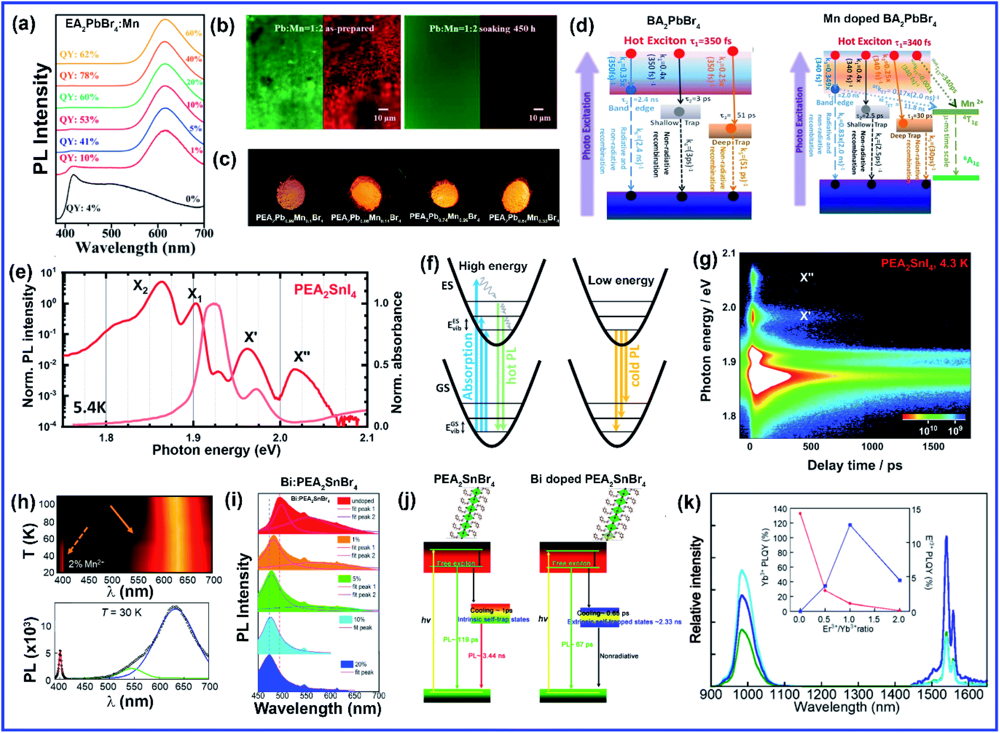 | ||
| Fig. 8 (a) Normalized PL spectra of Mn2+ doped EA2PbBr4 perovskites with different Mn2+ concentrations. Reprinted with permission from ref. 72. Copyright 2019, American Chemical Society. (b) PL microscopy images of as-prepared and water soaked 2% Mn doped PEA2PbI4-PVDF films. Reprinted with permission from ref. 77. Copyright 2021, Wiley VCH. (c) Photograph of PEA2Pb1−xMnxBr4 powders with increasing Mn doping concentration under UV light. Reprinted with permission from ref. 74. Copyright 2019, American Chemical Society. (d) Schemes of energy transfer of undoped and Mn doped BA2PbBr4 perovskites. Reprinted with permission from ref. 110. Copyright 2019, American Chemical Society. (e) Normalized PL spectra and the corresponding normalized absorbance spectra of PEA2SnI4 at 5.4 K, (f) relevant excitonic transitions of the absorbance, hot, and cold luminescence of PEA2SnI4/PEA2PbI4/PEA2SnBr4 perovskites and (g) streak camera plot of the PEA2SnI4 PL at 4.3 K. Reprinted with permission from ref. 111. Copyright 2021, Wiley VCH. (h) PL intensity mapping of 2% Mn2+ doped EA2PbBr4 with emission wavelength and temperature. Band edge and STE emission are shown in the map by dashed arrow and solid arrow, respectively along with the Mn2+ emission band centered at 630 nm. The lower row shows the PL spectrum of Mn2+ doped EA2PbBr4 at T = 30 K with the multiple peak fit. Reprinted with permission from ref. 112. Copyright 2020, American Chemical Society. (i) Room temperature PL spectra of Bi doped PEA2SnBr4 with different Bi concentrations and (j) schematic of the excited state dynamics of undoped and Bi doped perovskites. Reprinted with permission from ref. 85. Copyright 2019, Elsevier. (k) PL spectra of Yb and Er codoped quasi 2D CsPbCl3 layers and inset shows the variation in PL QY of Yb and Er luminescence. Reprinted with permission from ref. 91. Copyright 2020, AIP Publishing. | ||
:1 Li-doped crystal than in the undoped one.87 Thus, Li-doping introduced more trap states in the perovskite crystals and thus showed stronger STE emission. Interestingly, negative thermal quenching behavior was observed in 2D XL maps of (PEA)2PbBr4 crystals which was further enhanced with Li doping. The ratio of integrated intensity ratios between the minima (∼10 K) and the maxima (∼350 K) increased with Li-ion concentrations (0.23 for undoped to 0.42 for 1:1 Li doped), indicating the relatively wide-range emission stability of Li–(PEA)2PbBr4 crystals.87 Incorporation of a lanthanide material in a 2D perovskite crystal also introduced interesting optical features. Introduction of a Eu3+ tetrakis β-diketonate complex in NMA2PbBr4 perovskite greatly reduced the absorbance below 275 nm though its excitonic absorption didn't change much indicating a strong disruption of the NMA stacking pattern and modifications in the intermolecular forces holding the crystal.88 The PL spectra of undoped NMA2PbBr4 exhibited narrowband excitonic emission at 389 nm and a secondary band peaked at 564 nm related to the NMA triplet emission. Eu3+ doping introduced five sharp emission bands peaking at 576, 589, 611, 648, and 697 nm characteristic of the Eu3+ intra-configurational transitions 5D0 → 7FJ (J = 0–4) which appeared overlapped with the triplet emission.88 The presence of all five Eu3+ transitions indicated strong deviations from the inversion symmetry due to strong octahedral distortion, the spatial arrangement of the nearest neighbors (e.g., organic cations), and the symmetry group of the crystal lattice.88 The role of the NMA triplet was to sensitize the lanthanide material since Eu3+ transitions were not observed in Eu doped BA2PbClxBr4−x and PEA2PbClxBr4−x systems where the organic cation does not have an accessible triplet level. The excitonic emission in Eu3+ doped NMA2PbBr4 followed the power-law dependence I = PK (where I and P indicate the PL intensity and excitation power, respectively) with K ≲ 1, indicating the contribution from nonradiative decay paths, such as transfer to the NMA triplet state or recombination in the defects in the excitonic emission which limits the PL QY (∼0.3%). By protecting Eu3+ with the ligands, strongly enhanced 5D0 → 7F2 transition at 611 nm was observed resulting in a bright red emission of NMA2PbBr4:Eu(L) and NMA2PbCl2Br2:Eu(L). The Eu complex doped 2D perovskite showed narrower emission and PL QYs of 9 and 13% for NMA2PbBr4:Eu(L) and NMA2PbCl2Br2:Eu(L), respectively, which were ∼30-fold enhanced compared to that of EuCl3 doped NMA2PbBr4 perovskite.88 Miyasaka's group reported highly sensitized luminescence of Yb3+ by quasi 2D-CsPbCl3 with NIR PL QYs exceeding 130% due to the quantum cutting effect.91 The band-edge excitonic emission of CsPbCl3 at 415 nm from its cubic-phase perovskite lattice completely disappeared in the layer structure with intercalating Yb3+ and the NIR luminescence from Yb3+ strongly appeared at 983 nm by the excitation of CsPbCl3 at 300 nm.91 Er3+ and Yb3+ codoped 2D CsPbCl3 film exhibited two NIR emission bands at 983 nm and 1540 nm corresponding to 2F5/2 → 2F7/2 transition of Yb3+ and 4I13/2 → 4I15/2 transition from Er3+, respectively, but doping with only Er3+ could not be sensitized by CsPbCl3 (Fig. 8(k)).91 The PL QY of Yb luminescence dramatically decreased from 132.9% to 1.5% with increasing Er doping concentration, as shown in the inset of Fig. 8(k). Thus, Yb3+ worked both as an energy acceptor for quantum cutting and an energy donor to Er3+ in the codoped system, but the direct energy transfer from CsPbCl3 to Er3+ was ineffective.91 Energy transfer of Yb3+ to Er3+ was also confirmed by time decay profiles as the decay profiles of Yb3+ luminescence became faster from 1.69 ms to 0.18 ms by the intercalation of Er3+ ions.91 Doping Ce3+ and Tb3+ in the 2D layered structure of MAPbBr3 perovskite allowed the tuning of the PL peak by 0.337 eV and 0.587 eV, respectively, to the deep blue region.92 Recently, by incorporating 70 mol% CeBr3 in the perovskite crystal, our group achieved a deep blue emitting nanoplatelet with 100% QY, narrow linewidth (∼24 nm), and a color coordinate of (0.145, 0.054) closely matching with the standard color Rec. 2020 (0.131, 0.046) specification, making it one of the most efficient perovskite blue light emitters reported to date.92 The enhancement of PL QY through Ce doping was attributed to the formation of shallow trap states near the conduction band, which enriched the conduction band edge states instead of trapping the carriers.92 However, Ce3+ and Tb3+ emission could not be observed as MAPbBr3 was not able to sensitize the lanthanide materials.
5.3 X-site doping induced optoelectronic properties
Optical tunability through halide exchange is one of the most significant advantages of perovskites. The PL emission of halide perovskites is generally red shifted, or the bandgap is systematically reduced with the change in halide composition from Cl to Br to I due to the change of the valence orbital of halides from 3p to 4p to 5p.37 Apart from tuning the PL spectra, the inclusion of CsCl in quasi-2D perovskite film resulted in a decrease in FWHM, accompanied by a decrease in PL intensity.94 The KI doped mixed halide (C6H9C2H4NH3)2PbBr4 perovskite finely tuned the exciton binding energy from 120 to 200 meV with increasing doping concentrations from 0 to 20 vol% resulting in the decline of photogenerated charge carrier lifetimes, originating from the increased effective masses of charge carriers with the iodine doping.95 The exciton PL emission peak was tuned from blue (∼416 nm) to green (∼518 nm) through halide exchange using KI doping. Along with this, interestingly, the Stokes shift parameter decreased from 150 to 30 meV with an increase in the corresponding KI doping concentration level from 5 to 60 vol%, respectively, in a mixed halide (C6H9C2H4NH3)2PbBr4 perovskite indicating a reduction in non-radiative recombination loss.95 Interlayer triplet energy transfer was observed to occur in the mixed halide (1,5-NDA)PbX4 DJ perovskite film.98 The (1,5-NDA)PbBr4 composition showed very weak emission from the inorganic exciton centered at 425 nm and dominated the broad unstructured low-energy emission corresponding to the naphthalene triplet excimer due to complete transfer of the exciton energy from the lead bromide layer to naphthalene by a large driving force of around 0.36 eV. The driving force for triplet transfer was reduced in the mixed halide compositions with incorporation of iodine resulting in dual emission from both the inorganic exciton and naphthalene species as the close alignment between inorganic exciton band and naphthalene triplet facilitated reversible triplet energy transfer across the interface. Finally, for the (1,5-NDA)PbI4 composition, triplet transfer was inhibited by an energy barrier of around 0.18 eV and exhibited emission exclusively from the inorganic exciton centered at 510 nm.986. Applications
6.1 Solar cells
2D metal halide perovskites, which were extensively studied in the 1990s, have proven to be very promising in improving the stability of perovskite photovoltaics in comparison to 3D perovskites.46,53,54,114 In contrast to 3D perovskites, the poor PCE of layered perovskites is attributed to the inhibition of out-of-plane charge transport by the organic cations, which act like insulating spacing layers between the conducting inorganic slabs.50 It is reported that this issue can be overcome by producing thin films of near-single-crystalline quality, in which the crystallographic planes of the inorganic perovskite component have a strongly preferential out-of-plane alignment with respect to the contacts in planar solar cells to facilitate efficient charge transport resulting in an increase in the PCE of (BA)2(MA)3Pb4I13 perovskite solar cell from 4.73% to 12.52% with no hysteresis and greater humidity tolerance compared to its 3D counterpart.50 The efficiency of the 2D (BA)2(MA)3Pb4I13 perovskite solar cell was further improved to 13.7% through 5% Cs+ doping with greatly enhanced tolerance to humidity due to the perfectly controlled crystal orientation, increased grain size of 2D planes, superior surface quality, reduced trap-state density, enhanced charge-carrier mobility and charge-transfer kinetics (Fig. 9(a)).51 Chen et al. investigated further in this direction and slightly boosted the PCE to 13.92% by using Cu doped NiOx film as the hole transporting layer (HTL).52 High PCE of the doped device resulted from a high open circuit voltage (VOC) of 1.16 V and high current density of 17.57 mA cm−2 due to the efficient charge carrier shuttling and low recombination in the device (Fig. 9(b)).52 Recently, 10% Cs doping in the (BA2(MA)2Pb3I10) perovskite solar cell improved the efficiency from 7.98% to 10.11% with increase in conductivity from 2.14 to 2.56 mS m−1.53 | ||
| Fig. 9 (a) Cs doped 2D perovskite solar cell structure. Reprinted with permission from ref. 51. Copyright 2017, Royal Society of Chemistry. (b) Characteristic J–V curves of 2D: 5% Cs solar cell device. Reprinted with permission from ref. 52. Copyright 2019, Wiley VCH. (c) Variation in VOC and HI of the alkali cation doped perovskite solar cell. Reprinted with permission from ref. 54. Copyright 2020, American Chemical Society. (d) Variation in J–V curves with both backward and forward voltage scan directions of a fluorinated cation-based perovskite solar cell. Reprinted with permission from ref. 116. Copyright 2020, Wiley VCH. (e) Relationship of VOC with the light intensity of a 2D perovskite solar cell with different organic cations. Reprinted with permission from ref. 55. Copyright 2020, American Chemical Society. (f) Photo and ambient stability of doped and undoped devices. Reprinted with permission from ref. 97. Copyright 2021, American Chemical Society. | ||
Though the efficiency of 2D perovskites is still nowhere close to the 3D one, a thin layer of 2D perovskite can act as a capping layer for 3D perovskite solar cells which not only mitigates the stability issue but also improves the photovoltaic performance. 2D perovskites with mixed cations were reported to be more beneficial than single cation-based perovskite solar cells. Bach et al. further achieved improved efficiency and decrease in hysteresis from 14.8% to 4.7% with alkali doping in 2D perovskites due to suppressed out-of-plane packing.54 Among K+ and Rb+, the incorporation of the small K+ cation showed a higher hysteresis index (HI) in 3D/2D perovskite solar cells due to mobilization under an external voltage as compared to the larger cation Rb+, but K+ was a more effective passivator than Rb+ in the 2D perovskite (Fig. 9(c)).54 To use the benefits of both the cations, they codoped K+ and Rb+ in a 2D perovskite and achieved a negligible hysteresis index of 4.7% with an average PCE of 21.1%. 2D passivation of 3D perovskite films using a mixed composition of two bulky alkylammonium halide compounds (n-BAI and i-BAI) resulted in highly efficient mixed dimensional 2D/3D perovskite solar cells with an impressive open-circuit voltage of 1.21 V.57 The dual-isomer alkylammonium cation-passivation device also achieved the highest steady-state efficiency (≈23.1%) measured at the maximum power point, compared to ≈22.4% for n-BAI and 22.1% for i-BAI.57 Introducing F5PEA into the PEA-based 2D metal halide perovskite improves the efficiency (from 7.64% to 10.24%) with significantly improved stability (maintaining more than 80% of its original efficiency after 30 days under a RH of 45% without encapsulation).58 The improved stability of the mixed cation device was ascribed to the aryl–perfluoroaryl interaction, a strong noncovalent interaction that improved the structural stability of the 2D halide perovskite as well as the device stability.58 Additionally, depositing fresh electrodes on the same devices after 30 days could recover 92% of the initial efficiency.58 In another study, it was shown that an F5PEA-based 2D perovskite layer deposited on top of the 3D perovskite absorber layer enhanced the hole collection and reduced the surface recombination, leading to improved device efficiency (PCE > 22%) and high stability (retaining 90% of its efficiency during photovoltaic operation for 1000 h in humid air under simulated sunlight).115 In the same line, Zhu et al. introduced F5PEA+ to partially replace PEA+ with a strong noncovalent interaction between two bulky cations in a wide bandgap 2D perovskite, which was used as a passivating agent in a 3D FAPbI3 perovskite solar cell device. The efficiency of the device increased from 19.58% in mono cation PEA+-based device to 21.10% in the mixed cation device due to enhanced current density along with improved stability (Fig. 9(d)).116 Br doping in the 2D PEAI derived perovskite capping layer also passivated the interfacial defects resulting in a decrease in interfacial charge recombination and increase in carrier lifetime which could improve the overall PCE of 2D capped 3D perovskite solar cells with improved stability.117
The fluorinated organic spacer was reported to enhance the efficiency of the device due to enhancement in the dipole moment and the dielectric constant of the organic molecules, which facilitated efficient charge separation. Zhu et al. have reported that the efficiency could be improved from 9.66% to 13.64% by using parafluoro-PEA as the spacer due to enhanced orbital interactions and charge transport across adjacent inorganic layers as well as increased carrier lifetime and reduced trap density.118 You et al. systematically studied the effects of the monofluorinated position on the PEA cations on the photovoltaic performance of the 2D RP perovskite solar cells, and showed a promising efficiency of 10.89% using the para-fluorine substituted PEA as the spacer.119 However, the fluorinated spacer in the FA-based 2D perovskite device yielded a champion efficiency of 17.37%, which is much higher than that of the unfluorinated one (12.92%) due to enhanced mobility, and reduced trap density.106
Sn-based 3D perovskite solar cells have not reached the desired efficiency yet and degrade very fast due to the oxidation of Sn2+ in the air or even in an inert atmosphere.120–122 In contrast, employing Sn-based 2D layered perovskites is reported to be a promising approach for photovoltaic applications with high stability.123–125 Sn-based 2D perovskite solar cells containing shorter alkyl chain lengths showed higher PCE in contrast to the device containing longer alkyl chain lengths due to the better crystallographic orientation and the device retained 80% of its initial efficiency after 14 days in a N2 atmosphere without encapsulation which further implied the feasibility of employing different alkyl chains to suppress Sn2+ oxidation and thereby to improve their stability.55 Open circuit voltage (VOC) is said to be strongly dependent on the light intensity, and the trap-assisted Shockley–Read–Hall (SRH) recombination, when the slope of the VOC value is greater than kBT/q, and bimolecular recombination dominates when the slope of VOC is equal to kBT/q. The BA-based device displayed lower leakage current and the lowest slope in the plots of VOCversus natural logarithmic light intensity, suggesting that the shorter alkyl chain length-based device possessed reduced trap-assisted recombination compared to the longer chain length (OA and DA) ones (Fig. 9(e)).55
Interfacial engineering is an effective way to modulate the energy band alignment and reduce the interfacial charge recombination in perovskite solar cells. Gradient band alignment was achieved in an FA4Pb5I16 DJ perovskite by FABr treatment.96 Post FABr treatment, the PCE of the device increased from 13.78% to 16.75% due to a significant increase in open-circuit voltage. Br doping not only enhanced the device performance but also increased the operational stability by maintaining 93% of its initial PCE after aging under the RH range of 15–20% for 1600 h, 91% after aging at 60 °C for 400 h, and 66% after aging under one sun illumination for 400 h.96 Therefore, halide exchange in 2D perovskites facilitates carrier extraction, transfer, and collection, which remarkably suppress nonradiative recombination due to the construction of gradient band alignment, improved crystallinity, and reduced defect density.96 GABr treatment in (GA)2MA4Pb5I16 2D films also not only improved the PCE of the device from 15.6% to 19.3% due to the decrease in trap density and trap-assisted Shockley–Read–Hall recombination, but also improved the stability of the device as well by maintaining the PCE up to 94% of its original value after being exposed at 10 ± 5% RH for 3000 h (Fig. 9(f)).97 Hence, the DJ 2D perovskite solar cell exhibits better performance compared to the RP one. To improve the performance of 2D perovskite solar cells, it is necessary to reduce the crystal defects and improve the crystal orientation which will allow efficient charge transport (Table 4).
| Sample | Dopant | V OC (V) | J SC (mA cm−2) | PCE (%) | Stability | Ref. |
|---|---|---|---|---|---|---|
| (BA)2(MA)3Pb4I13 | Cs+ | 1.08 | 19.95 | 13.7 | 10% decrease in PCE after 1400 h exposure in 30% RH and 15% decrease after being stored at 85% RH for 24 h | 51 |
| (BA)2(MA)3Pb4I13 | Cs+ | 1.16 | 17.57 | 13.92 | 39% decrease in PCE after 240 h of aging at 35–40% RH under ambient conditions | 52 |
| BA2(MA)2Pb3I10 | Cs+ | 1.19 | 13.34 | 10.11 | After 300 h of exposure to air (55% RH), the PCE retention rate was 61% | 53 |
| BA2(Cs0.05FA0.79MA0.16)Pb2(I0.83Br0.17)7/3D perovskite | Rb and K | 1.17 | 23.1 | 21.1 | Preserves 90% of the original PCE after aging for 160 h under RH of 85% | 54 |
| (n-BA)2PbI4/3D perovskite | iso-BAI | 1.21 | 24.29 | 23.1 | After 100 h of light soaking, device retained 94% of the initial PCE | 57 |
| (PEA)2PbI4 | F5-PEA | 1.15 | 14.55 | 10.24 | Maintained more than 80% of its original efficiency after 30 days at an RH of 45% | 58 |
| (PEA)2PbI4/3D FAPbI3 | F5-PEA | 1.19 | 21.65 | 21.10 | About 17% degradation in PCE after 720 h (45–60% RH) | 116 |
| (PEA)2PbI4/3D perovskite | Br | 1.14 | 23.60 | 20.07 | Retained 88% of its initial efficiency after 80 days (38% RH) | 117 |
| (PhFA)2MAn−1PbnI3n+1−xClx/3D MAPbI3 | Fluorinated p-FPhFA | 1.13 | 20.54 | 17.37 | Maintained 99% of its initial PCE after 3000 h stored in a N2-filled glovebox | 106 |
| FA4Pb5I16 | Br | 1.10 | 19.69 | 16.75 | Retained 93% of its initial PCE for 1600 h at a RH of 15–20% in the dark | 96 |
| (GA)2MA4Pb5I16 | Br | 1.17 | 21.9 | 19.3 | Maintained the PCE up to 94% of its original value after being exposed to RH of 10% for 3000 h | 97 |
6.2 Light emitting diodes
Though 2D perovskites have wide PL spectra, due to the high exciton binding energy, stable structure and quantum confinement effect, they can be very useful for light emitting applications. Directly suppressing the exciton–phonon interaction by introducing rigid structures is proved to be an effective strategy to improve the optical properties of 2D perovskites, which were first realized in 2D perovskite LEDs (PeLEDs) by Wang et al. through Mn2+ doping in (BIZ)2PbI4 films (Fig. 10(a)).69 A Mn2+ doped 2D (BIZ)2PbI4 perovskite LED exhibited lower leakage current density below the turn-on voltage (∼2.9 V), a relatively higher current density above the turn-on voltage, 10 times brighter luminance compared to the device with undoped 2D perovskite due to suppressed electron–phonon interaction.69 The external quantum efficiency (EQE) of the device increased from 0.01% to 0.045% by Mn doping as a result of enhanced free exciton electroluminescence (EL). Extremely low film thickness is a necessary condition for the 2D PeLEDs because of the low conductivity of the wide-band-gap lead bromide perovskite. However, thinner perovskites suffer from a high degree of trap-assisted recombination. Mn-doping can substantially reduce the defect-related emission and improve the EQE. The LED fabricated with Mn-doped single-layered NMA2PbBr4 was almost one order of magnitude more efficient than the undoped one.71 Very high luminescent, stable orange-red emitting LED was fabricated with PEA2Pb0.74Mn0.26Br4 perovskites with PL at 600 nm, luminance 71890 cd m−2, and luminous efficiency 23 lm W−1, which was higher than that of Mn-doped 3D perovskite devices (Fig. 10(b)).74 The device retained 90% of the initial emission intensity after continuously working at 20 mA for 350 h.74 A highly stable, yellow lighting application was illustrated recently on a large-area PEA2PbI4:Mn-PVDF film with a maximum luminance value of 250 cd m−2 and nearly equal green and red emission intensities with a color coordinate of (0.47, 0.50) due to its high transmittance under UV light excitation.77 The device showed excellent stability under harsh conditions as it retained about 75% of the original luminance intensity after 24 h of continuous operation.77 Also, its luminance was unaffected after immersing in water at room temperature for 450 h and exposing under harsh conditions of 85 °C/85% relative humidity for 120 h (Fig. 10(c)).77 The water and thermal stability of the device came from the hydrophobicity of PVDF and PEA+ in 2D perovskites and inhibited thermal decomposition with the protection of compact PVDF molecule networks.77
 | ||
| Fig. 10 (a) Device structure of 2D PeLED. Reprinted with permission from ref. 69. Copyright 2019, American Chemical Society. (b) PL spectrum of a Mn doped 2D perovskite LED (adopted from ref. 74). Reprinted with permission from ref. 74. Copyright 2019, American Chemical Society. (c) Variation in luminance with time of the PEA2PbI4:2Mn-PVDF yellow LED device after being exposed in water and at 85 °C/85% relative humidity. Reprinted with permission from ref. 77. Copyright 2021, Wiley VCH. (d) Variation in EQE with current density of the quasi-2D PeLED with different PEA:NMA ratios. Reprinted with permission from ref. 63. Copyright 2021, American Chemical Society. (e) EL spectra of the Mn2+ ion doped (PEA)2PbBr4 white LED with different CCTs. Reprinted with permission from ref. 78. Copyright 2021, Royal Society of Chemistry. (f) Scheme of field induced charge injection process in a mixed halide PeLED. Reprinted with permission from ref. 127. Copyright 2021, American Chemical Society. | ||
In general, red-emitting perovskite materials are synthesized based on Br/I mixed halide perovskites, but they suffer from stability issues since the mixed-halide perovskite systems are susceptible to halide segregation induced by the electric field under continuous operation. Jiang et al. fabricated spectrally stable Rb–Cs alloyed quasi 2D pure blue-emitting PeLED with an emission peak at 475 nm, EQE of 1.35%, and a lifetime of 14.5 min.126 Very recently, Shao et al. fabricated pure-red PeLEDs based on quasi-2D perovskites by simultaneously incorporating PEA and NMA cations.63 The PeLEDs with PEA:NMA molar ratio of 5:5 exhibited a pure-red (635 nm) EL with a CIE coordinate (0.709, 0.285) approaching the Rec. 2020 specification, a maximum EQE of 12.41% and high brightness of 1452.6 cd m−2, which is among the best performance for quasi-2D pure-red PeLEDs (Fig. 10(d)).63 Deng et al., for the first time, used Zn2+-doped (C8H17NH3)2SnBr4 perovskite as a yellow phosphor for UV pumped LED fabrication. The CIE coordinates, color rendering index (CRI), and correlated color temperature (CCT) of the fabricated yellow LED were measured to be (0.5060, 0.4542), 75, and 2455 K, respectively. By adjusting the Mn doping concentration, Bai et al. demonstrated “warm” and “cold” Mn2+ ion-doped (PEA)2PbBr4 and CsPb(Cl/Br)3 white LEDs with the corresponding CIE coordinates of (0.39, 0.37) and (0.30, 0.31) and CCTs of 3614 K and 7043 K, respectively (Fig. 10(e)).78 Recently, we reported a Ce3+ doped 2D MAPbBr3 perovskite white LED.92 To fabricate the Ce doped MAPbBr3 white LED, MAPb0.3Ce0.7Br3 and rhodamine B were mixed with PMMA solution separately and sequentially deposited on a low-cost commercial UV emitting chip (400 nm) and dried under ambient conditions.92 The white light converter demonstrated a CCT of 5437 K, CRI of 73, and luminescence efficiency of 79.6 lm W−1 at 2.74 V, CIE coordinates of (0.334, 0.326) which are remarkably close to the standard white light (0.33, 0.33).92
The spectral instability of mixed halide PeLEDs due to anion migration obstructs their uses in practical applications. Recently, a plausible mechanism of spectral instability of mixed halide layered perovskite LEDs was presented by Kim et al.127 The Br and I ions in the mixed halide perovskite film move in random directions due to thermal excitation; after the application of electric field the ions take their preferred directions as a result of Coulomb attraction. As iodide encounters a significantly lower out-of-plane diffusion barrier, iodide-rich domains are formed near the HTL, while the remaining portion of the emitting layer turns into the bromide-rich domains (Fig. 10(f)).127 This created a very selective pathway of charge transfer. Injected holes in the HTL are selectively transferred to the iodine rich surface whereas injected electrons in the ETL can be transported to either iodine or bromine rich domains. Therefore, excitons are formed near the iodine rich surface resulting in a red shifted EL. With the incorporation of iodine, the EL spectra of the PEA2MA4Pb5Br16 perovskite LED were red shifted by more than 100 nm as compared to the film PL as well as the device PL, whereas the device PL and EL of the pure bromide-based perovskite LED were consistent with each other.127 This suggested that the luminescence of mixed halide perovskite devices is mostly due to exciton recombination in the iodine rich surface due to halide redistribution during device operation. Thus, suppressing the ion migration is very crucial in improving the spectral and operational stability of mixed halide layered perovskite devices.
6.3 X-ray imaging
Currently, there is great demand for medical imaging, scientific research, and security in the scintillator market, and the requirement of very high temperature in synthesizing bulk crystal scintillators hinders their uses. Li doped (PEA)2PbBr4 scintillator film was reported to be very efficient in demonstrating the X-ray scintillation imaging application.87 The Li-(PEA)2PbBr4 film with a thickness of 67 μm was prepared by blow-drying the film with a hot air flow in the last stage of spin-coating resulting in high transparency and homogeneity, despite some small surface ripples, and was used for the first time as a scintillator film.87 Li-ion dopant could increase the light yield up to 11000 ph per MeV while maintaining a primary decay time (11 ns) under 662 keV gamma-ray radiation.87 The Li-(PEA)2PbBr4 scintillator could also detect alpha particles and discriminate alpha particles and gamma-rays.87 Hence, 2D perovskite is a very promising radiation detector, and further investigation will lead to various applications beyond solar cells and LEDs.
7. Conclusion: challenges and future scope
In this review, we have summarized the general background of 2D perovskites and discussed the progress in the doping of 2D layered perovskites along with its influence on the optoelectronic properties and applications. First, we have discussed various doping strategies in 2D layered perovskites based on A, B, and X sites with their effects on the crystal structures. Next, we have deliberated on the effect of doping on the optoelectronic properties and stability of 2D perovskites. Finally, the progress of doped 2D perovskite-based devices has been discussed. Even though significant progress has been made in the doping of 2D perovskites, a deeper understanding of the mechanism of doping and an appropriate strategy of efficient doping in 2D layered metal halide perovskites are still in their infancy. We will conclude this review by addressing a few challenges and the future scope that the community is expected to address to obtain new insights into the doping process.7.1 Facile synthesis and mass production
A thorough investigation is needed on the actual doping mechanism in layered perovskites to understand the dopant location inside the host lattice, the byproduct of a particular synthesis method, and the ways to remove the byproducts. Halide doping often results in the formation of phase-segregated phases, which hinders the carrier transport, thus limiting the device performance. The development of new strategies should be emphasized to prevent phase segregation especially for higher layer thickness (n > 5) perovskite structures as they are thermodynamically less favorable.128 An in-depth understanding of the passivation mechanism will be conducive to developing better doping strategies. More research needs to be carried out to identify the kind of defects and the depth of trap states which will help in quantifying the advantageous role of doping in passivating defects. A vast library of organic molecules can be incorporated in the 2D perovskite layers, and it has a vast potential for hybrid applications.The performance of photovoltaic devices critically depends on the high quality, large area thin film, or single crystal. Further optimization and control is needed for the tailored synthesis of large-scale doped 2D perovskite single crystals, which is not achieved yet. Further development or modification is highly desirable to extend the deposition techniques of 2D perovskite thin films from a one-step spin coating method to various large-scale industrial fabrication techniques, such as slot-die coating, inkjet-printing, and aerosol-jet printing.
7.2 Some fundamental aspects of doping dependent properties
Uncontrolled doping may lead to phase transitions in solids. Phase transition in 2D perovskites has a more diverse effect on the crystal structure, and optoelectronic properties of 2D perovskites than their 3D counterpart as large organic spacers strongly modulate the transition. High-temperature phase transition may increase the conformational and dynamic disorder of the large organic cations, thus it increases the perovskite layer symmetry and the low-temperature phase transition is intimately linked to lattice parameter change and inorganic octahedral tilting of the 2D perovskite layer.129 Thus, A site doping will distinctly affect the high temperature phase transition and B/X site doping will have a greater impact on low-temperature phase transition. Therefore, a detailed study is necessary on the effect of doping on the phase transition of 2D perovskites and how it affects the electronic band structure, electron–phonon coupling, charge carrier dynamics, and light–matter interactions.Next, various mechanical properties such as out-of-plane and in-plane Young's modulus in 2D perovskites vary with metal–halide bond length, type of organic spacer cation, the interaction of organic cations, and the perovskite phase. Thus, there is an opportunity to explore the impact of doping at different sites on the mechanical properties of layered perovskites and to understand the correlation between mechanical and physical properties.
Strong spin–orbit coupling in 2D perovskites causes Rashba and Dresselhaus effects due to the interplay between time-reversal symmetry and the lack of spatial inversion symmetry which result in some peculiarities in their electronic band structure. Also, some researchers found a nontrivial dependence of the Rashba effect on the thickness and composition of 2D perovskites. Future study is needed to probe these spin-dependent effects in doped 2D perovskites and integrate them appropriately in spintronics.
7.3 Doping dependent optoelectronic properties and applications beyond solar cells
Though the PL QY of Br-based layered perovskites is improved considerably, light emission efficiency is still poor for Cl and I based perovskites. The fundamental reason behind the poor performance remains undiscovered. Mn2+ doping is the only widely studied strategy to replace Pb; other possible dopants can be explored (especially the lanthanide materials) to introduce interesting features and extend the PL emission up to the NIR region. Though electron–phonon coupling is extremely sensitive to structural disorder and defects in 2D perovskites, which in turn effects the carrier mobility, carrier ionization etc., there is very limited knowledge available about the correlation of electron–phonon coupling and structural properties. The exciton kinetics is substantially different in 2D perovskites, especially magnetically doped 2D perovskite systems compared to 3D perovskites as hot excitons play a crucial role in determining the energy transfer rate. Very few studies have been reported on the photophysics of 2D perovskites. In some cases, unexpectedly long-lived hot exciton emission is observed whose origin still remains elusive. More extensive investigation is needed on the effect of doping on the electronic properties of 2D perovskites, particularly shifting of the Fermi level. Recently, paramagnetic doping has shown significant success in 3D metal halide perovskites, which is entirely unexplored in layered perovskites. Paramagnetic doping will open new insights with interesting magnetic properties, which may reveal exciting avenues for research in spintronics, magnetic data storage, etc.Next, 2D perovskites with larger n-values tend to orient perpendicularly to the substrate, which can be beneficial for vertical structure photodetector devices as contact electrodes can be in direct contact with the semiconductor inorganic sheet layer and not the insulating organic layer. However, photodetector applications of pristine 2D perovskites and the doped ones are little explored, and it should be investigated in detail for practical applications. The effect of variations on the chain lengths of capping layers, composition and orientation of mixed halide 2D perovskites on the performance of LEDs need to be investigated in detail.
In essence, fundamental and in-depth understanding of the issues discussed above is crucial to fully utilize the potential of doping strategies in the field of 2D layered perovskites. The A-site doping strategy with various organic ligands and alkali cations has cut a brilliant figure in 2D perovskite solar cells and the B-site doping strategy with Mn2+ ions has shown considerable improvement in 2D PeLEDs. Since ferroelectric to paraelectric phase transition is observed in 2D perovskites, a detailed analysis on the interplay between ferroelectricity and semiconductor physics in two dimensions can be explored using doped 2D perovskites, which may help in the emergence of novel self-powered ultrathin optoelectronic devices, such as ferroelectric field-effect transistors. There is still a vast potential for improvement in the light emission and electrical properties of 2D perovskites. The stability of 2D layered perovskites is much higher than that of 3D bulk perovskites; hence, doped 2D perovskites with less cytotoxicity yet retaining high efficiency will play a prominent role in developing the field of perovskites commercially. The doping techniques should be extended to other optoelectronic devices such as ultrafast photodetectors, X-ray detectors, low-threshold lasers, X-ray imaging, bio-imaging, neuromorphic devices etc. We believe that future research on various dopants with simple and controlled techniques will contribute greatly to the next generation of functional optoelectronic devices with 2D layered perovskites as an active layer or passivating layer on 3D perovskite film.
Author contributions
Sumaiya Parveen: conceptualization, formal analysis, investigation, resources, writing – original draft, review & editing. P. K. Giri: conceptualization, formal analysis, funding acquisition, investigation, project administration, supervision, resources, validation, writing – review & editing.Conflicts of interest
The authors declare no conflicts of interest.References
- A. Kojima, K. Teshima, Y. Shirai and T. Miyasaka, J. Am. Chem. Soc., 2009, 131, 6050–6051 CrossRef CAS PubMed.
- A. Kojima, M. Ikegami, K. Teshima and T. Miyasaka, Chem. Lett., 2012, 41, 397–399 CrossRef CAS.
- M. R. Leyden, L. K. Ono, S. R. Raga, Y. Kato, S. Wang and Y. Qi, J. Mater. Chem. A, 2014, 2, 18742–18745 RSC.
- G. Xing, N. Mathews, S. Sun, S. S. Lim, Y. M. Lam, M. Grätzel, S. Mhaisalkar and T. C. Sum, Science, 2013, 342, 344–347 CrossRef CAS PubMed.
- G. Xing, N. Mathews, S. S. Lim, N. Yantara, X. Liu, D. Sabba, M. Grätzel, S. Mhaisalkar and T. C. Sum, Nat. Mater., 2014, 13, 476–480 CrossRef CAS PubMed.
- Y. Fang, Q. Dong, Y. Shao, Y. Yuan and J. Huang, Nat. Photonics, 2015, 9, 679–686 CrossRef CAS.
- L. Protesescu, S. Yakunin, M. I. Bodnarchuk, F. Krieg, R. Caputo, C. H. Hendon, R. X. Yang, A. Walsh and M. V. Kovalenko, Nano Lett., 2015, 15, 3692–3696 CrossRef CAS PubMed.
- D. H. Chun, Y. J. Choi, Y. In, J. K. Nam, Y. J. Choi, S. Yun, W. Kim, D. Choi, D. Kim, H. Shin, J. H. Cho and J. H. Park, ACS Nano, 2018, 12, 8564–8571 CrossRef CAS PubMed.
- H. Li and W. Zhang, Chem. Rev., 2020, 120, 9835–9950 CrossRef CAS PubMed.
- Y. Rong, Y. Hu, A. Mei, H. Tan, M. I. Saidaminov, S. I. Seok, M. D. McGehee, E. H. Sargent and H. Han, Science, 2018, 361, eaat8235 CrossRef PubMed.
- L. Meng, J. You and Y. Yang, Nat. Commun., 2018, 9, 5265 CrossRef CAS PubMed.
- S. Zhang and G. Han, Prog. Energy, 2020, 2, 022002 CrossRef.
- G. Grancini, C. Roldán-Carmona, I. Zimmermann, E. Mosconi, X. Lee, D. Martineau, S. Narbey, F. Oswald, F. De Angelis, M. Graetzel and M. K. Nazeeruddin, Nat. Commun., 2017, 8, 15684 CrossRef CAS PubMed.
- C. Ge, Y. Z. B. Xue, L. Li, B. Tang and H. Hu, Front. Mater., 2020, 7, 601179 CrossRef.
- L. Xu, S. Yuan, H. Zeng and J. Song, Mater. Today Nano, 2019, 6, 100036 CrossRef.
- G. Rose, De Novis Quibusdam Fossilibus Quae in Montibus Uraliis InveniunturBerolini, typis A. G. Schadii, 1839 Search PubMed.
- C. K. Møller, Nature, 1958, 182, 1436 CrossRef.
- D. Weber, Z. Naturforsch. B Chem. Sci., 1978, 33, 862–865 CrossRef.
- D. Weber, Z. Naturforsch. B Chem. Sci., 1978, 33, 1443–1445 CrossRef.
- C.-H. Lu, G. V. Biesold-McGee, Y. Liu, Z. Kang and Z. Lin, Chem. Soc. Rev., 2020, 49, 4953–5007 RSC.
- R. L. Milot, R. J. Sutton, G. E. Eperon, A. A. Haghighirad, J. Martinez Hardigree, L. Miranda, H. J. Snaith, M. B. Johnston and L. M. Herz, Nano Lett., 2016, 16, 7001–7007 CrossRef CAS PubMed.
- F. Zhang, H. Lu, J. Tong, J. J. Berry, M. C. Beard and K. Zhu, Energy Environ. Sci., 2020, 13, 1154–1186 RSC.
- S. Ahmad and X. Guo, Chin. Chem. Lett., 2018, 29, 657–663 CrossRef CAS.
- B. V. Beznosikov and K. S. Aleksandrov, Crystallogr. Rep., 2000, 45, 792–798 CrossRef.
- T. M. Koh, V. Shanmugam, J. Schlipf, L. Oesinghaus, P. Müller-Buschbaum, N. Ramakrishnan, V. Swamy, N. Mathews, P. P. Boix and S. G. Mhaisalkar, Adv. Mater., 2016, 28, 3653–3661 CrossRef CAS PubMed.
- A. a. O. El-Ballouli, O. M. Bakr and O. F. Mohammed, J. Phys. Chem. Lett., 2020, 11, 5705–5718 CrossRef CAS PubMed.
- M. C. Weidman, M. Seitz, S. D. Stranks and W. A. Tisdale, ACS Nano, 2016, 10, 7830–7839 CrossRef CAS PubMed.
- S. Das Adhikari and N. Pradhan, Front. Mater., 2020, 7, 206 CrossRef.
- C. Ortiz-Cervantes, P. Carmona-Monroy and D. Solis-Ibarra, ChemSusChem, 2019, 12, 1560–1575 CrossRef CAS PubMed.
- D. B. Straus and C. R. Kagan, J. Phys. Chem. Lett., 2018, 9, 1434–1447 CrossRef CAS PubMed.
- S. A. Veldhuis, P. P. Boix, N. Yantara, M. Li, T. C. Sum, N. Mathews and S. G. Mhaisalkar, Adv. Mater., 2016, 28, 6804–6834 CrossRef CAS PubMed.
- P. Fu, Q. Shan, Y. Shang, J. Song, H. Zeng, Z. Ning and J. Gong, Sci. Bull., 2017, 62, 369–380 CrossRef CAS.
- W. Tian, C. Zhao, J. Leng, R. Cui and S. Jin, J. Am. Chem. Soc., 2015, 137, 12458–12461 CrossRef CAS PubMed.
- J. A. Sichert, Y. Tong, N. Mutz, M. Vollmer, S. Fischer, K. Z. Milowska, R. García Cortadella, B. Nickel, C. Cardenas-Daw and J. K. Stolarczyk, Nano Lett., 2015, 15, 6521–6527 CrossRef CAS PubMed.
- M. Kumagai and T. Takagahara, Phys. Rev. B: Condens. Matter Mater. Phys., 1989, 40, 12359–12381 CrossRef CAS PubMed.
- A. Miyata, A. Mitioglu, P. Plochocka, O. Portugall, J. T.-W. Wang, S. D. Stranks, H. J. Snaith and R. J. Nicholas, Nat. Phys., 2015, 11, 582 Search PubMed.
- S. Parveen, K. K. Paul and P. K. Giri, ACS Appl. Mater. Interfaces, 2020, 12, 6283–6297 CrossRef CAS PubMed.
- S. Parveen, K. K. Paul, R. Das and P. K. Giri, J. Colloid Interface Sci., 2019, 539, 619–633 CrossRef CAS PubMed.
- H. Mathieu, P. Lefebvre and P. Christol, Phys. Rev. B: Condens. Matter Mater. Phys., 1992, 46, 4092–4101 CrossRef PubMed.
- L. C. Andreani and A. Pasquarello, Phys. Rev. B: Condens. Matter Mater. Phys., 1990, 42, 8928–8938 CrossRef CAS PubMed.
- J. Even, L. Pedesseau, C. Katan, M. Kepenekian, J.-S. Lauret, D. Sapori and E. Deleporte, J. Phys. Chem. C, 2015, 119, 10161–10177 CrossRef CAS.
- D. B. Straus, S. Hurtado Parra, N. Iotov, J. Gebhardt, A. M. Rappe, J. E. Subotnik, J. M. Kikkawa and C. R. Kagan, J. Am. Chem. Soc., 2016, 138, 13798–13801 CrossRef CAS PubMed.
- A. Brehier, R. Parashkov, J. S. Lauret and E. Deleporte, Appl. Phys. Lett., 2006, 89, 171110 CrossRef.
- M. Braun, W. Tuffentsammer, H. Wachtel and H. C. Wolf, Chem. Phys. Lett., 1999, 303, 157–164 CrossRef CAS.
- K. Ema, M. Inomata, Y. Kato, H. Kunugita and M. Era, Phys. Rev. Lett., 2008, 100, 257401 CrossRef CAS PubMed.
- D. B. Mitzi, C. A. Feild, W. T. A. Harrison and A. M. Guloy, Nature, 1994, 369, 467–469 CrossRef CAS.
- D. B. Mitzi, Prog. Inorg. Chem., 1999, 48, 1–121 CAS.
- D. B. Mitzi, S. Wang, C. A. Feild, C. A. Chess and A. M. Guloy, Science, 1995, 267, 1473 CrossRef CAS PubMed.
- S. Parveen, S. M. Obaidulla and P. K. Giri, Appl. Surf. Sci., 2020, 530, 147224 CrossRef CAS.
- H. Tsai, W. Nie, J.-C. Blancon, C. C. Stoumpos, R. Asadpour, B. Harutyunyan, A. J. Neukirch, R. Verduzco, J. J. Crochet, S. Tretiak, L. Pedesseau, J. Even, M. A. Alam, G. Gupta, J. Lou, P. M. Ajayan, M. J. Bedzyk, M. G. Kanatzidis and A. D. Mohite, Nature, 2016, 536, 312–316 CrossRef CAS PubMed.
- X. Zhang, X. Ren, B. Liu, R. Munir, X. Zhu, D. Yang, J. Li, Y. Liu, D.-M. Smilgies, R. Li, Z. Yang, T. Niu, X. Wang, A. Amassian, K. Zhao and S. Liu, Energy Environ. Sci., 2017, 10, 2095–2102 RSC.
- Q. Xu, K. Meng, Z. Liu, X. Wang, Y. Hu, Z. Qiao, S. Li, L. Cheng and G. Chen, Adv. Mater. Interfaces, 2019, 6, 1901259 CrossRef CAS.
- T.-C. Hsieh, C.-Y. Shih, Y.-C. Chao, I. C. Cheng and J.-Z. Chen, RSC Adv., 2021, 11, 20200–20206 RSC.
- C. Liu, J. Sun, W. L. Tan, J. Lu, T. R. Gengenbach, C. R. McNeill, Z. Ge, Y.-B. Cheng and U. Bach, Nano Lett., 2020, 20, 1240–1251 CrossRef CAS PubMed.
- F. Li, Y. Xie, Y. Hu, M. Long, Y. Zhang, J. Xu, M. Qin, X. Lu and M. Liu, ACS Energy Lett., 2020, 5, 1422–1429 CrossRef CAS.
- Z. Yao, Y. Zhou, X. Yin, X. Li, J. Han, M. Tai, Y. Zhou, J. Li, F. Hao and H. Lin, CrystEngComm, 2018, 20, 6704–6712 RSC.
- M. A. Mahmud, T. Duong, Y. Yin, J. Peng, Y. Wu, T. Lu, H. T. Pham, H. Shen, D. Walter, H. T. Nguyen, N. Mozaffari, G. D. Tabi, Y. Liu, G. Andersson, K. R. Catchpole, K. J. Weber and T. P. White, Small, 2020, 16, 2005022 CrossRef CAS PubMed.
- J. Hu, I. W. H. Oswald, H. Hu, S. J. Stuard, M. M. Nahid, L. Yan, Z. Chen, H. Ade, J. R. Neilson and W. You, ACS Mater. Lett., 2019, 1, 171–176 CrossRef CAS.
- X. Li, J. Hoffman, W. Ke, M. Chen, H. Tsai, W. Nie, A. D. Mohite, M. Kepenekian, C. Katan, J. Even, M. R. Wasielewski, C. C. Stoumpos and M. G. Kanatzidis, J. Am. Chem. Soc., 2018, 140, 12226–12238 CrossRef CAS PubMed.
- Y. Li, J. V. Milić, A. Ummadisingu, J.-Y. Seo, J.-H. Im, H.-S. Kim, Y. Liu, M. I. Dar, S. M. Zakeeruddin, P. Wang, A. Hagfeldt and M. Grätzel, Nano Lett., 2019, 19, 150–157 CrossRef CAS PubMed.
- S. Ahmad, P. Fu, S. Yu, Q. Yang, X. Liu, X. Wang, X. Wang, X. Guo and C. Li, Joule, 2019, 3, 794–806 CrossRef CAS.
- B.-E. Cohen, Y. Li, Q. Meng and L. Etgar, Nano Lett., 2019, 19, 2588–2597 CrossRef CAS PubMed.
- L. Yang, Y. Zhang, J. Ma, P. Chen, Y. Yu and M. Shao, ACS Energy Lett., 2021, 6, 2386–2394 CrossRef CAS.
- W. Liu, Q. Lin, H. Li, K. Wu, I. Robel, J. M. Pietryga and V. I. Klimov, J. Am. Chem. Soc., 2016, 138, 14954–14961 CrossRef CAS PubMed.
- W. J. Mir, M. Jagadeeswararao, S. Das and A. Nag, ACS Energy Lett., 2017, 2, 537–543 CrossRef CAS.
- A. Biswas, R. Bakthavatsalam and J. Kundu, Chem. Mater., 2017, 29, 7816–7825 CrossRef CAS.
- L. Dou, A. B. Wong, Y. Yu, M. Lai, N. Kornienko, S. W. Eaton, A. Fu, C. G. Bischak, J. Ma, T. Ding, N. S. Ginsberg, L.-W. Wang, A. P. Alivisatos and P. Yang, Science, 2015, 349, 1518 CrossRef CAS PubMed.
- M. H. P. Usman, R. Bakthavatsalam and J. Kundu, ChemistrySelect, 2018, 3, 6585–6595 CrossRef CAS.
- L. Zhang, T. Jiang, C. Yi, J. Wu, X.-K. Liu, Y. He, Y. Miao, Y. Zhang, H. Zhang, X. Xie, P. Wang, R. Li, F. Gao, W. Huang and J. Wang, J. Phys. Chem. Lett., 2019, 10, 3171–3175 CrossRef CAS PubMed.
- Z.-J. Li, E. Hofman, A. H. Davis, A. Khammang, J. T. Wright, B. Dzikovski, R. W. Meulenberg and W. Zheng, Chem. Mater., 2018, 30, 6400–6409 CrossRef CAS.
- D. Cortecchia, W. Mróz, S. Neutzner, T. Borzda, G. Folpini, R. Brescia and A. Petrozza, Chem, 2019, 5, 2146–2158 CAS.
- B. Luo, Y. Guo, X. Li, Y. Xiao, X. Huang and J. Z. Zhang, J. Phys. Chem. C, 2019, 123, 14239–14245 CrossRef CAS.
- T. Sheikh and A. Nag, J. Phys. Chem. C, 2019, 123, 9420–9427 CrossRef CAS.
- C. Sun, Z. Gao, Y. Deng, H. Liu, L. Wang, S. Su, P. Li, H. Li, Z. Zhang and W. Bi, ACS Appl. Mater. Interfaces, 2019, 11, 34109–34116 CrossRef CAS PubMed.
- L. Hou, Y. Zhu, J. Zhu, X. Li, F. Zeng, T. Yang, Y. Gong, J. Shen and C. Li, Adv. Mater. Interfaces, 2021, 8, 2002175 CrossRef CAS.
- Q. Ba, A. Jana, L. Wang and K. S. Kim, Adv. Funct. Mater., 2019, 29, 1904768 CrossRef CAS.
- J. Dang, Z. Yang, W. Guo, Y. Ji, H. Wang, J. Deng and M. Wang, Adv. Mater. Interfaces, 2021, 8, 2100560 CrossRef CAS.
- X. Gao, X. Shen, D. Xue, X. Li, P. Lu, M. Lu, C. Li, W. W. Yu and X. Bai, Mater. Chem. Front., 2021, 5, 937–943 RSC.
- H. Zhang, J. Yao, Y. Yang and H. Fu, Chem. Mater., 2021, 33, 2847–2854 CrossRef CAS.
- L. Lanzetta, J. M. Marin-Beloqui, I. Sanchez-Molina, D. Ding and S. A. Haque, ACS Energy Lett., 2017, 2, 1662–1668 CrossRef CAS.
- P. Fu, M. Huang, Y. Shang, N. Yu, H.-L. Zhou, Y.-B. Zhang, S. Chen, J. Gong and Z. Ning, ACS Appl. Mater. Interfaces, 2018, 10, 34363–34369 CrossRef CAS PubMed.
- X. Zhang, C. Wang, Y. Zhang, X. Zhang, S. Wang, M. Lu, H. Cui, S. V. Kershaw, W. W. Yu and A. L. Rogach, ACS Energy Lett., 2019, 4, 242–248 CrossRef CAS.
- A. Wang, Y. Guo, Z. Zhou, X. Niu, Y. Wang, F. Muhammad, H. Li, T. Zhang, J. Wang, S. Nie and Z. Deng, Chem. Sci., 2019, 10, 4573–4579 RSC.
- Y. Liu, A. Wang, J. Wu, C. Wang, Z. Li, G. Hu, S. Sui, J.-X. She, W. Meng, W. Li and Z. Deng, Mater. Adv., 2021, 2, 1320–1327 RSC.
- R. Zhang, X. Mao, P. Cheng, Y. Yang, S. Yang, T. Wumaier, W. Deng and K. Han, J. Energy Chem., 2019, 36, 1–6 CrossRef CAS.
- F. Lyu, X. Zheng, Y. Wang, R. Shi, J. Yang, Z. Li, J. Yu and B.-L. Lin, J. Mater. Chem. A, 2019, 7, 15627–15632 RSC.
- A. Xie, C. Hettiarachchi, F. Maddalena, M. E. Witkowski, M. Makowski, W. Drozdowski, A. Arramel, A. T. S. Wee, S. V. Springham, P. Q. Vuong, H. J. Kim, C. Dujardin, P. Coquet, M. D. Birowosuto and C. Dang, Commun. Mater., 2020, 1, 37 CrossRef.
- D. Cortecchia, W. Mróz, G. Folpini, T. Borzda, L. Leoncino, A. L. Alvarado-Leaños, E. M. Speller and A. Petrozza, Chem. Mater., 2021, 33, 2289–2297 CrossRef CAS PubMed.
- W. J. Mir, T. Sheikh, H. Arfin, Z. Xia and A. Nag, NPG Asia Mater., 2020, 12, 9 CrossRef CAS.
- T. J. Milstein, D. M. Kroupa and D. R. Gamelin, Nano Lett., 2018, 18, 3792–3799 CrossRef CAS PubMed.
- A. Ishii and T. Miyasaka, J. Chem. Phys., 2020, 153, 194704 CrossRef CAS PubMed.
- S. Parveen, P. K. Prasanna, S. Chakraborty and P. K. Giri, J. Mater. Chem. C, 2021, 9, 2437–2454 RSC.
- M. Fazayeli, M. Khatamian and G. Cruciani, CrystEngComm, 2020, 22, 8063–8071 RSC.
- B. Liu, X. Zou, D. Chen, T. Liu, Y. Zuo, J. Zheng, Z. Liu and B. Cheng, Tsinghua Sci. Technol., 2021, 26, 496–504 CAS.
- M. Rahil, P. Rajput, D. Ghosh and S. Ahmad, ACS Appl. Electron. Mater., 2020, 2, 3199–3210 CrossRef CAS.
- P. Su, L. Bai, H. Bi, B. Liu, S. Chen, D. Lee, H. Yang, C. Chen, Z. Zang and J. Chen, J. Power Sources, 2021, 506, 230213 CrossRef CAS.
- Y. Huang, Y. Li, E. L. Lim, T. Kong, Y. Zhang, J. Song, A. Hagfeldt and D. Bi, J. Am. Chem. Soc., 2021, 143, 3911–3917 CrossRef CAS PubMed.
- Y. L. Lin and J. C. Johnson, J. Phys. Chem. Lett., 2021, 12, 4793–4798 CrossRef CAS PubMed.
- Akriti, E. Shi, S. B. Shiring, J. Yang, C. L. Atencio-Martinez, B. Yuan, X. Hu, Y. Gao, B. P. Finkenauer, A. J. Pistone, Y. Yu, P. Liao, B. M. Savoie and L. Dou, Nat. Nanotechnol., 2021, 16, 584–591 CrossRef CAS PubMed.
- E. Shi, B. Yuan, S. B. Shiring, Y. Gao, Akriti, Y. Guo, C. Su, M. Lai, P. Yang, J. Kong, B. M. Savoie, Y. Yu and L. Dou, Nature, 2020, 580, 614–620 CrossRef CAS PubMed.
- C. R. Roy, D. Pan, Y. Wang, M. P. Hautzinger, Y. Zhao, J. C. Wright, Z. Zhu and S. Jin, J. Am. Chem. Soc., 2021, 143, 5212–5221 CrossRef CAS PubMed.
- W. T. M. Van Gompel, R. Herckens, K. Van Hecke, B. Ruttens, J. D'Haen, L. Lutsen and D. Vanderzande, Chem. Commun., 2019, 55, 2481–2484 RSC.
- N. Marchal, W. Van Gompel, M. C. Gélvez-Rueda, K. Vandewal, K. Van Hecke, H.-G. Boyen, B. Conings, R. Herckens, S. Maheshwari, L. Lutsen, C. Quarti, F. C. Grozema, D. Vanderzande and D. Beljonne, Chem. Mater., 2019, 31, 6880–6888 CrossRef CAS.
- M. C. Gélvez-Rueda, W. T. M. Van Gompel, R. Herckens, L. Lutsen, D. Vanderzande and F. C. Grozema, J. Phys. Chem. Lett., 2020, 11, 824–830 CrossRef PubMed.
- J. V. Passarelli, C. M. Mauck, S. W. Winslow, C. F. Perkinson, J. C. Bard, H. Sai, K. W. Williams, A. Narayanan, D. J. Fairfield, M. P. Hendricks, W. A. Tisdale and S. I. Stupp, Nat. Chem., 2020, 12, 672–682 CrossRef CAS PubMed.
- Q. Li, Y. Dong, G. Lv, T. Liu, D. Lu, N. Zheng, X. Dong, Z. Xu, Z. Xie and Y. Liu, ACS Energy Lett., 2021, 6, 2072–2080 CrossRef CAS.
- A. Arramel, A. D. Fauzi, X. Yin, C. S. Tang, M. H. Mahyuddin, M. F. Sahdan, M. Aminah, D. Onggo, G. Shukri, C. Diao, H. Wang, M. D. Birowosuto, A. T. S. Wee and A. Rusydi, Commun. Mater., 2021, 2, 70 CrossRef.
- W. Peng, J. Yin, K.-T. Ho, O. Ouellette, M. De Bastiani, B. Murali, O. El Tall, C. Shen, X. Miao, J. Pan, E. Alarousu, J.-H. He, B. S. Ooi, O. F. Mohammed, E. Sargent and O. M. Bakr, Nano Lett., 2017, 17, 4759–4767 CrossRef CAS PubMed.
- Z. Fang, K. Wu, L. Wang, D. Xu, W. Wang, Y. Lin, X. Liu and C. Sun, J. Lumin., 2021, 237, 118155 CrossRef CAS.
- R. Bakthavatsalam, A. Biswas, M. Chakali, P. R. Bangal, B. P. Kore and J. Kundu, J. Phys. Chem. C, 2019, 123, 4739–4748 CrossRef CAS.
- S. Kahmann, H. Duim, H.-H. Fang, M. Dyksik, S. Adjokatse, M. Rivera Medina, M. Pitaro, P. Plochocka and M. A. Loi, Adv. Funct. Mater., 2021, 31, 2103778 CrossRef CAS.
- S. Sarang, W. Delmas, S. Bonabi Naghadeh, V. Cherrette, J. Z. Zhang and S. Ghosh, J. Phys. Chem. Lett., 2020, 11, 10368–10374 CrossRef CAS PubMed.
- H. Long, X. Peng, J. Lu, K. Lin, L. Xie, B. Zhang, L. Ying and Z. Wei, Nanoscale, 2019, 11, 21867–21871 RSC.
- X. Zhao, T. Liu and Y.-L. Loo, Adv. Mater., 2021, 2105849 Search PubMed.
- Y. Liu, S. Akin, L. Pan, R. Uchida, N. Arora, J. V. Milić, A. Hinderhofer, F. Schreiber, A. R. Uhl, S. M. Zakeeruddin, A. Hagfeldt, M. I. Dar and M. Grätzel, Sci. Adv., 2019, 5, eaaw2543 CrossRef CAS PubMed.
- J. Y. Ye, J. Tong, J. Hu, C. Xiao, H. Lu, S. P. Dunfield, D. H. Kim, X. Chen, B. W. Larson, J. Hao, K. Wang, Q. Zhao, Z. Chen, H. Hu, W. You, J. J. Berry, F. Zhang and K. Zhu, Sol. RRL, 2020, 4, 2000082 CrossRef CAS.
- Y. Lv, Y. Shi, X. Song, J. Liu, M. Wang, S. Wang, Y. Feng, S. Jin and C. Hao, ACS Appl. Mater. Interfaces, 2018, 10, 31755–31764 CrossRef CAS PubMed.
- F. Zhang, D. H. Kim, H. Lu, J.-S. Park, B. W. Larson, J. Hu, L. Gao, C. Xiao, O. G. Reid, X. Chen, Q. Zhao, P. F. Ndione, J. J. Berry, W. You, A. Walsh, M. C. Beard and K. Zhu, J. Am. Chem. Soc., 2019, 141, 5972–5979 CrossRef CAS PubMed.
- J. Hu, I. W. H. Oswald, S. J. Stuard, M. M. Nahid, N. Zhou, O. F. Williams, Z. Guo, L. Yan, H. Hu, Z. Chen, X. Xiao, Y. Lin, Z. Yang, J. Huang, A. M. Moran, H. Ade, J. R. Neilson and W. You, Nat. Commun., 2019, 10, 1276 CrossRef PubMed.
- Q. Tai, X. Guo, G. Tang, P. You, T.-W. Ng, D. Shen, J. Cao, C.-K. Liu, N. Wang, Y. Zhu, C.-S. Lee and F. Yan, Angew. Chem., Int. Ed., 2019, 58, 806–810 CrossRef CAS PubMed.
- H.-C. Wang, W. Wang, A.-C. Tang, H.-Y. Tsai, Z. Bao, T. Ihara, N. Yarita, H. Tahara, Y. Kanemitsu, S. Chen and R.-S. Liu, Angew. Chem., Int. Ed., 2017, 56, 13650–13654 CrossRef CAS PubMed.
- A. B. F. Vitoreti, S. Agouram, M. Solis de la Fuente, V. Muñoz-Sanjosé, M. A. Schiavon and I. Mora-Seró, J. Phys. Chem. C, 2018, 122, 14222–14231 CrossRef CAS PubMed.
- Y. Liao, H. Liu, W. Zhou, D. Yang, Y. Shang, Z. Shi, B. Li, X. Jiang, L. Zhang, L. N. Quan, R. Quintero-Bermudez, B. R. Sutherland, Q. Mi, E. H. Sargent and Z. Ning, J. Am. Chem. Soc., 2017, 139, 6693–6699 CrossRef CAS PubMed.
- D. H. Cao, C. C. Stoumpos, T. Yokoyama, J. L. Logsdon, T.-B. Song, O. K. Farha, M. R. Wasielewski, J. T. Hupp and M. G. Kanatzidis, ACS Energy Lett., 2017, 2, 982–990 CrossRef CAS.
- I. Zimmermann, S. Aghazada and M. K. Nazeeruddin, Angew. Chem., Int. Ed., 2019, 58, 1072–1076 CrossRef CAS PubMed.
- Y. Jiang, C. Qin, M. Cui, T. He, K. Liu, Y. Huang, M. Luo, L. Zhang, H. Xu, S. Li, J. Wei, Z. Liu, H. Wang, G.-H. Kim, M. Yuan and J. Chen, Nat. Commun., 2019, 10, 1868 CrossRef PubMed.
- Y. Nah, O. Allam, H. S. Kim, J. I. Choi, I. S. Kim, J. Byun, S. O. Kim, S. S. Jang and D. H. Kim, ACS Nano, 2021, 15, 1486–1496 CrossRef CAS PubMed.
- L. Mao, C. C. Stoumpos and M. G. Kanatzidis, J. Am. Chem. Soc., 2019, 141, 1171–1190 CrossRef CAS PubMed.
- J.-C. Blancon, J. Even, C. C. Stoumpos, M. G. Kanatzidis and A. D. Mohite, Nat. Nanotechnol., 2020, 15, 969–985 CrossRef CAS PubMed.
| This journal is © The Royal Society of Chemistry 2022 |