
Structured and functionalized organic semiconductors for chemical and biological sensors based on organic field effect transistors†
Yujing
Wang
,
Qi
Gong
 and
Qian
Miao
*
and
Qian
Miao
*
Department of Chemistry, the Chinese University of Hong Kong, Shatin, New Territories, Hong Kong, China. E-mail: miaoqian@cuhk.edu.hk
First published on 2nd June 2020
Abstract
One of the most promising applications of organic field-effect transistors (OFETs) is chemical and biological sensing. In order to achieve highly sensitive and selective detection of a broad array of analytes, the organic semiconductor layer in an OFET is tailored with rationally designed physical structures and chemical functionalities. This article reviews representative studies on structured and functionalized organic semiconductors after a brief introduction to OFET-based chemical and biological sensors. Finally, we reach conclusions on the achievements and challenges in this research field and provide an outlook for the development in the near future.
 Yujing Wang | Yujing Wang was born in China in 1995. She received her Bachelor's degree in chemistry and materials science from the University of Science and Technology of China (USTC) in 2017. She is currently a PhD candidate in Prof. Qian Miao's group at the Chinese University of Hong Kong (CUHK). Her research interests focus on the synthesis of functionalized polycyclic aromatic molecules and their applications in electronic devices. |
 Qi Gong | Qi Gong was born in China in 1997. She received her BS degree in chemistry from the University of Science and Technology of China (USTC) in 2019. Now she is a PhD student in the research group of Prof. Qian Miao in the Chemistry Department of the Chinese University of Hong Kong (CUHK). Her research focuses on gas sensors based on organic field effect transistors. |
 Qian Miao | Prof. Qian Miao graduated from the University of Science and Technology of China with a BSc degree in 2000. He received his PhD degree from Columbia University in 2005 under the direction of Prof. Colin Nuckolls, and then did postdoctoral research with Prof. Fred Wudl at the University of California, Los Angeles. He joined the Chinese University of Hong Kong as an assistant professor in 2006, and was promoted to Associate Professor in 2012 and Professor in 2016. His research interests include design and synthesis of novel polycyclic aromatic molecules with interesting structures and useful applications, and development of high-performance organic semiconductor materials and devices using tools from organic synthesis, supramolecular chemistry and surface chemistry. |
Introduction
This review aims to provide an overview of strategies to tailor organic semiconductors with rationally designed physical structures and chemical functionalities to develop chemical and biological sensors based on organic field effect transistors (OFETs). An OFET typically consists of a thin film of organic semiconductors, three electrodes (gate, drain and source) and a dielectric layer between the semiconductor and the gate electrode as shown in Fig. 1a. An OFET essentially acts as an on/off switch, where the electrical current flowing between the drain and source electrodes (IDS) is controlled by the voltage between the gate and source electrodes (VGS) under an imposed bias between the drain and source electrodes (VDS). The velocity of charge carriers (holes or electrons for p- or n-type organic semiconductors, respectively) in OFETs is quantified by the field effect mobility, which is the most important parameter to characterize the performance of OFETs. OFETs are promising platforms for various types of sensors1–4 with a unique combination of advantages. First, the electronic input and output characteristics of OFETs can be modulated by a variety of physical and chemical stimuli through different mechanisms. For example, light or heat can greatly affect the conductivity of organic semiconductors by altering the density and mobility of charge carriers, and mechanical work can influence the gate voltage applied to the conduction channel. Second, OFET-based sensors can be fabricated on flexible substrates over large area at low cost because organic semiconductors, unlike conventional inorganic semiconductors, are mechanically flexible and can be processed with solution-based methods. Third, organic semiconductors can be conveniently tailored through organic synthesis or surface functionalization to provide specific recognition sites or reactive groups for target analytes. Fourth, compared with the sensors based on resistance change in a two-terminal device, OFET-based sensors can have lower detection limits and higher sensitivity due to the inherent signal amplification function of transistors. As a result, OFET-based sensors not only circumvent the need for bulky and expensive equipment by combining sensory electrical output with easy device fabrication, but also promise soft and biocompatible electronics for wearable and implantable devices.5–9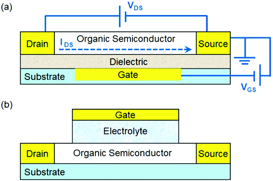 | ||
| Fig. 1 (a) Schematic structure of an OFET with the applied voltage (VDS and VGS) and source–drain current (IDS); and (b) schematic structure of an EGOFET. | ||
The above advantages of organic semiconductors for chemical and biological sensors based on field effect transistors (FETs) are, to some degree, shared by carbon nanotubes and graphene, which are graphitic nanocarbons and arguably “organic”. However, organic semiconductors still exhibit their own strengths and weaknesses in comparison to graphitic nanocarbons. For example, organic semiconductors are more broadly functional themselves and have largely variable morphologies, but have lower charge carrier mobility than graphitic nanocarbons. Organic semiconductors may be more convenient to fabricate in printable form, while graphitic carbons can give higher mechanical strength. An excellent summary comparison of organic semiconductors with graphitic nanocarbons for FET-based chemical and biological sensors is given by Katz and coworkers in a recent review.10
For construction of chemical and biological sensors, two device configurations of OFETs have been widely used. One is the conventional OFET (Fig. 1a), where the organic semiconductor layer is exposed to the environment, and the other is the electrolyte-gated OFET (EGOFET),11 where the gate dielectric in the conventional OFET is replaced by an electrolyte and, as a result, the organic semiconductor layer is in ionic contact with a gate electrode via an electrolyte as shown in Fig. 1b. When a conventional OFET is exposed to the environment, environmental chemical and biological species (i.e. analytes) may occur at the surface of organic semiconductors, or at the grain boundaries between crystallites that make up a polycrystalline semiconductor film, or at interfaces between organic semiconductors and dielectrics or electrodes. These analyte molecules or ions can induce local electric fields, disrupt the molecular packing of organic semiconductors, trap mobile charge carriers by localizing them on the analyte molecules, or cause doping by charge transfer. At the electrolyte–organic semiconductor interface in an EGOFET, the applied gate voltage induces formation of an electrical double layer, which enables current modulation through electrostatic doping of the conduction channel. For the purpose of chemical and biological sensing, the most commonly used electrolyte is an aqueous solution. If the organic semiconductors in the conduction channel are electrochemically active, the application of a gate bias induces a reversible redistribution of ions within the transistor channel and the electrolyte. As a result, the device becomes an organic electrochemical transistor (OECT), which has already been extensively reviewed in the literature12,13 and thus is not covered herein. In order to realize selective detection of chemical and biological analytes, an EGOFET needs to be functionalized with specific groups to recognize or react with chosen analytes and the possible sites of functionalization include the organic semiconductor, gate and electrolytes.14 Chemical events at these sites are transduced to electrical signals because molecular recognition or chemical reactions can lead to changes in the surface potential or capacitance, or induce charge redistribution. In order to avoid overlap with the published reviews10,15–19 on OFET-based sensors, this review focuses on representative strategies to tailor organic semiconductors in conventional OFETs and EGOFETs to detect chemical and biological analytes sensitively and selectively. In the following discussions, these studies are roughly classified into two aspects. One is structured organic semiconductors, which are designed to have nanometer or micrometer-sized structures to enhance effective interactions between organic semiconductors and analytes. The other is functionalized organic semiconductors, where molecular recognition units or chemical reaction sites are introduced into semiconductors through physical adsorption or chemical modification.
The key parameters that determine the performance of an OFET-based chemical/biological sensor include the sensitivity, detection limit and selectivity. The sensitivity can be represented as either the absolute sensitivity or relative sensitivity. The absolute sensitivity is defined as ΔID/Canalyte, where ΔID denotes the absolute value of the net change in the drain current upon exposure to the analyte, and Canalyte denotes the concentration of analyte that results in the change of the drain current. The relative sensitivity is defined as (ΔID/ID,0)/Canalyte, where ID,0 denotes the initial drain current. For the purpose of comparison, the sensitivity in this review article is presented uniformly as the relative sensitivity, which is either already reported in the original literature or calculated by us from the reported change of the drain current and concentration of the analyte when the corresponding data are available. Typical units of relative sensitivity for OFET-based chemical/biological sensors include % ppm−1, % ppb−1, % μM−1 and % nM−1.
Structured organic semiconductors in OFET-based sensors
OFETs are interface devices, where the first few molecular layers of organic semiconductors at the semiconductor–dielectric interface form the conduction channel responsible for charge transport and current modulation by the gate voltage. Early OFET-based sensors were fabricated on vacuum-deposited films of organic semiconductors, which consisted of micrometer or sub-micrometer sized crystallites.20,21 In these sensing devices, the current modulation in response to the target analytes largely relies on chemical events that occur at the grain boundaries between the crystallites and are limited by diffusion of analyte molecules to the conduction channel of the OFET.22,23 In order to enhance the sensitivity of OFET-based sensors, nanometer or micrometer-sized structures, such as nanopores and monolayers, are introduced into the organic semiconductors to enhance the capability of capturing analyte molecules from the environment and to increase the opportunities of analyte molecules to interact with the conduction channel. It is worth noting that the structures designed to enhance the capability of organic semiconductors to capture analyte molecules may unfortunately compromise the pathways of charge transport. High-performance OFET-based sensors require a balance between efficient charge transport (reflected by a reasonably high field effect mobility) and capability of capturing analyte molecules.24 For easy reference, the performances of OFET-based sensors discussed in this section are summarized in Table 1. For OFET-based sensors that have organic semiconductors lacking specific functional groups to react or interact with analyte molecules, the most common target analytes are NH3 and NO2, which are an electron donor and an electron acceptor, respectively, toward common organic semiconductors.| Organic semiconductor | Physical structure | The way of measuring ID | Target analyte | Detection limit | Relative sensitivitya | Selectivity over chemicalsb | Ref. |
|---|---|---|---|---|---|---|---|
| Notes:a Relative sensitivity is measured at the detection limit if not otherwise noted.b Abbreviations: EtOH: ethanol, i-PrOH: isopropanol, THF: tetrahydrofuran, EA: ethyl acetate, DE: diethyl ether, DMMP: dimethyl methylphosphonate, DMC: dimethyl carbonate. | |||||||
| Pentacene | Porous film with a pore size of 50–150 nm | Real time test with fixed VG and VD | CH3OH | N/A | N/A | N/A | 25 |
| DNTT | Porous film with a pore size of 10 μm | Real time test with fixed VG and VD | NH3 | 10 ppb | 340% ppm−1 | HCl, H2O2, H2O, DMMP, DMC, hexane, CHCl3, EtOH, acetone | 26 |
| DPP2T-TT | Porous film with a pore size of 700 nm | Real time test with fixed VG and VD | NH3 | 1 ppb | 27.8% ppb−1 | NH3 | 27 |
| PBIBDF-BT | Porous film with a pore size of 100–400 nm | Real time test with fixed VG and VD | NH3 | 0.5 ppm | 9.98% ppm−1 (10 ppm) | i-PrOH, acetone, DE, EA, CHCl3, hexane, toluene | 28 |
| CuPc | Nanowire | Real time test with fixed VG and VD | SO2 | 0.5 ppm | 238% ppm−1 | N/A | 29 |
| ZnPc | Single nanobelt | Real time test with fixed VG and VD | NO2 | 50 ppb | 22% ppm−1 (10 ppm) | SO2 | 30 |
| H2S | 50 ppb | 91% ppm−1 (10 ppm) | SO2 | ||||
| AmBuPc | 7-Layer LB film | Output curve | NO2 | 10 ppm | N/A | N/A | 32 |
| Pentacene | Monolayer | Transfer curve | NO2 | 100 ppb | 650% ppm−1 (2 ppm) | CO, CO2 N2O, NH3 | 33 |
| CoPc | 4 Molecular layers | Real time test with fixed VG and VD | Organic volatiles | N/A | N/A | N/A | 34 |
| CuPc | Ultrathin film | Transfer curve | NO2 | 1 ppm | 65.8% ppm−1 | SO2, NH3, H2S | 35 |
| C10-DNTT | Monolayer crystals | Real time test with fixed VG and VD | NH3 | 10 ppb | 172% ppm−1 | Acetone, EtOH, H2, O2, NO | 37 |
| DTBDT-C6 | Microstripes of 6–11 nm thickness | Real time test with fixed VG and VD | NH3 | 10 ppm | 2% ppm−1 (50 ppm) | EtOH, i-PrOH, acetone, EA, heptane | 38 |
| 2R5T2R | Monolayer | Real time test with fixed VG and VD | Melamine solution | 0.01 ppm | N/A | N/A | 39 |
| NDI3HU-DTYM2 | Porous monolayer crystals | Real time test with fixed VG and VD | NH3 | 0.1ppb | 720% ppb−1 | i-PrOH, acetone, EtOH, THF, CHCl3 | 40 |
| HBC-COCl | Monolayer | Output curve | TCNQ (solution in DCM) | 1 mM | N/A | N/A | 41 |
| PTCDI-Ph/p-6P | Hetero-junction | Real time test with fixed voltage | NO2 | 5 ppm | 4.9% ppm−1 | N/A | 42 |
| PTCDI-Ph/p-6P/VOPc | Double hetero-junctions | Real time test with fixed voltage | NO2 | 5 ppm | 18% ppm−1 | N/A | 42 |
| TiOPc/F16CuPc | Hetero-junction | Real time test with fixed voltage | NO2 | 250 ppb | 478% ppm−1 (2 ppm) | N/A | 43 |
Porous films
Vertically oriented pores of micrometer or nanometer scale in films of organic semiconductors can not only enhance the capability of capturing analyte molecules by increasing the specific surface area but also allow more analyte molecules to penetrate to the conduction channel with greater coupling to the charge transport pathways. As a result, porous structures in organic semiconductor films enable sensors with higher sensitivity and faster response. Oh, Cho and coworkers fabricated porous films of pentacene by vacuum-deposition of pentacene (Fig. 2) on top of m-bis(triphenylsilyl)benzene (TSB3), which was vacuum-deposited onto an octadecyltrimethoxy-silane (OTS)-treated SiO2 substrate (Fig. 3a).25 The pores in the pentacene film ranged in size from 50 to 150 nm, and their depth was found to be similar to the thickness of the organic layers. The large number of nanopores in the pentacene film was attributed to the dewetting of TSB3 and the preferential growth of pentacene via diffusion onto TSB3 rather than OTS. In comparison to pentacene films without nanopore structures, these porous pentacene films exhibited significantly improved sensitivity toward methanol gas, which, however, was not reported in a quantitative manner. Huang and coworkers fabricated microporous films of dinaphtho[2,3-b:2′,3′-f]thieno[3,2-b]thiophene (DNTT as shown in Fig. 2) by using polystyrene microspheres with a diameter of 10 μm as templates, which were deposited on plasma-treated SiO2/Si substrates by a vacuum freeze-drying method (Fig. 3b).26 Upon exposure to 0.01 ppm NH3, the porous OFET of DNTT exhibited a decrease in the drain current with a relative sensitivity as high as 340% ppm−1, which is higher than that of the pristine OFET of DNTT (20% ppm−1) by an order of magnitude. The porous OFET also exhibited decent selectivity for NH3 (1 ppm) over a variety of chemical vapors (500 ppm) that are shown in Table 1. Diao and coworkers used a nanoporous insulating layer, which was prepared from a solution of poly(4-vinylphenol) (PVP) in THF with 4,4′-(hexafluoroisopropylidene)diphthalic anhydride (HDA) added as the cross-linking agent for PVP, as a template to form porous films of polymer and small molecule semiconductors with tunable pore sizes (50–700 nm) as shown in Fig. 3c.27 Upon exposure to 1 ppb NH3, the film of poly(diketopyrrolopyrrolethiophene-thieno[3,2,b]thiophene-thiophene) (DPP2T-TT as shown in Fig. 2) with 700 nm pores exhibited a relative sensitivity of 27.8% ppb−1, which is higher than that of the non-porous film of DPP2T-TT by 1.5 times. Qiu and coworkers prepared porous films of PBIBDF-BT (Fig. 2), an ambipolar polymer semiconductor, by spin coating a blend solution of PBIBDF-BT and poly(1,4-butylene adipate) (PBA) and subsequently removing PBA from the composite film with acetone.28 The pore size could be tuned by varying the percentage of PBA in the blends. The porous films of PBIBDF-BT with pore size ranging from 100 to 400 nm exhibited a relative sensitivity of greater than 80% ppm−1 in response to 10 ppm NH3 and decent selectivity for NH3 (10 ppm) over a variety of chemical vapors (500 ppm) that are shown in Table 1. However, the relationship between the pore size and the sensing performance of FETs was not reported.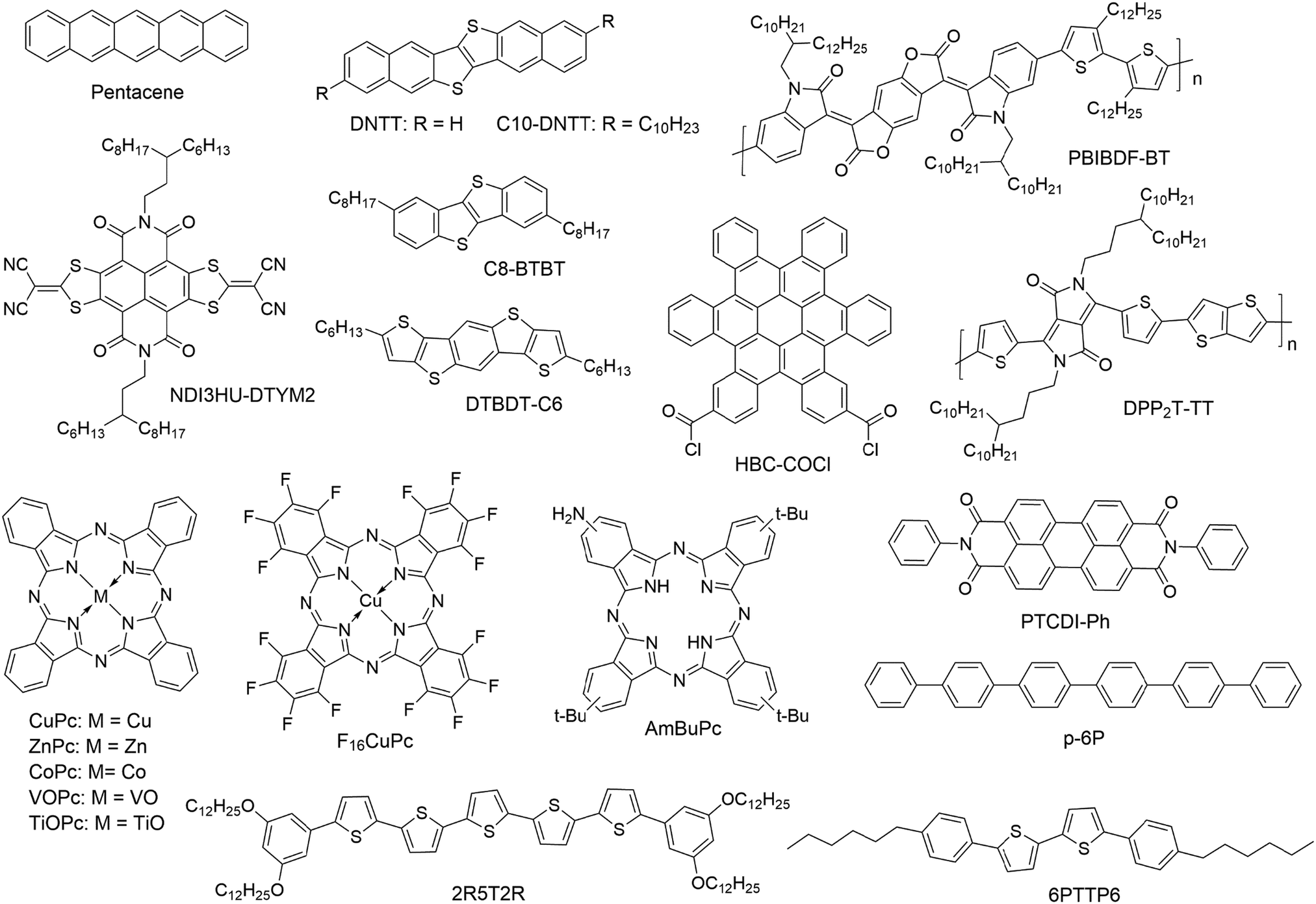 | ||
| Fig. 2 Structures of organic semiconductors that are tailored with designed physical structures. | ||
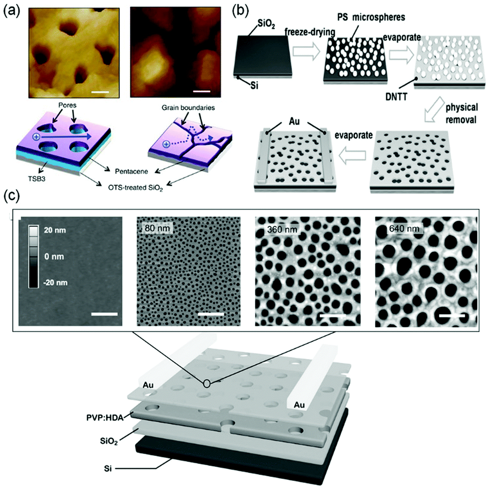 | ||
| Fig. 3 OFET-based sensors with porous films. (a) AFM images of pentacene (45 nm)/TSB3 (15 nm) and pentacene (45 nm) on OTS-treated SiO2, and a schematic diagram of the charge transport inside pentacene layers with and without TSB3. Scale bars, 200 nm. Reproduced with permission from ref. 25. Copyright 2014 Nature Publishing Group. (b) Schematic illustration of the fabrication procedure of the porous structure of DNTT. Reproduced with permission from ref. 26. Copyright 2017 Wiley. (c) Schematic of the nanoporous field-effect transistor device with DPP2T-TT as the active layer, and atomic force microscopy (AFM) height images of porous PVP:HDA templates, with pore diameters ranging from 0 to 640 nm. Scale bars, 1 μm. Reproduced with permission from ref. 27. Copyright 2017 Wiley. | ||
Nanowires and nanofibers
Single crystalline nanowires or nanofibers of organic semiconductors in a gas dielectric OFET present a useful device configuration for OFET-based sensors because they have the conduction channel exposed to the environment. Liu and coworkers in 2013 developed gas sensors for SO2 on the basis of a gas dielectric OFET, which had a single crystalline nanowire of copper phthalocyanine (CuPc as shown in Fig. 2) as the semiconductor (Fig. 4).29 This OFET-based sensor was able to detect SO2 at a sub-ppm level (0.5 ppm) with relative sensitivity as high as 238% ppm−1. In contrast, the CuPc single nanowire field effect transistors packaged with a poly(methyl methacrylate) (PMMA) dielectric did not show an obvious response toward SO2 of a concentration lower than 5 ppm in gas. Four years later, the same group reported similar gas dielectric OFETs containing a nanofiber of zinc phthalocyanine (ZnPc as shown in Fig. 2) as the semiconductor.30 This OFET-based gas sensor was able to detect NO2, H2S and SO2 with a lowest detectable concentration down to 50 ppb. In response to 10 ppm NO2, H2S and SO2, the relative sensitivity of this sensor is 22% ppm−1, 91% ppm−1 and 4% ppm−1, respectively. Moreover, this sensor can distinguish the above three gases when multiple field-effect parameters (field effect mobility, threshold voltage, and subthreshold swing) of the OFET are taken into consideration.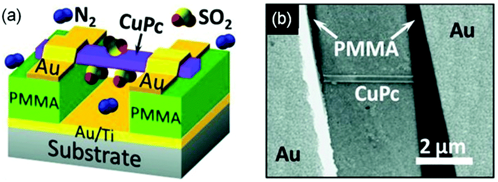 | ||
| Fig. 4 The schematic (a) and SEM (b) images of gas dielectric FETs based on CuPc nanowires. The channel length L = 3.3 μm, the width W = 210 nm (width of the nanowire), and the thickness of the dielectric d = 200 nm. Reproduced with permission from ref. 29. Copyright 2013 Wiley. | ||
Ultrathin films and monolayers
Reducing the thickness of the organic semiconductor layer in a conventional OFET-based sensor can shorten the distance that analyte molecules have to travel before they reach the effective conduction channel at the semiconductor–dielectric interface. Therefore, the conduction channel in an ultrathin OFET can have a better chance than a thick device of the same organic semiconductor to interact with analyte molecules, leading to higher sensitivity as well as shorter response time. On the other hand, ultrathin layers of organic semiconductors may suffer from poor environmental stability because of undesired interactions between organic semiconductors and environmental molecules (e.g. water) and also inferior margins for degradation over time. As a result, the optimized film thickness varies among different organic semiconductors for OFET-based chemical sensors to keep a good balance between sensitivity and stability.23 The extreme case of ultrathin films is a monolayer, which may suffer from low conductivity due to trapping and grain boundary effects. From a systematical study on vacuum-deposited ultrathin films of 5,5′-bis(4-hexylphenyl)-2,2′-bithiophene (6PTTP6 as shown in Fig. 2), Katz and coworkers demonstrated that the first monolayer of 6PTTP6 alone could not serve as the conduction channel, and the coverage of the second monolayer in the semiconductor film dominates the formation of the conduction channel.31 As a result, the optimized thickness of organic semiconductors in OFET-based sensors is not always a monolayer and, in fact, varies among different organic semiconductors. To the best of our knowledge, the strategy of using an ultrathin film of an organic semiconductor for OFET-based sensors was pioneered by Hu, Liu and coworkers, who used a 7-layer Langmuir–Blodgett film of amino-tri-tert-butyl-phthalocyanine (AmBuPc in Fig. 2) as the semiconductor layer for sensing NO2. This OFET responded to NO2 (10 to 70 ppm) in gas with a linearly increased drain current.32Jiang and coworkers fabricated monolayer OFETs of pentacene by vacuum-deposition of pentacene on top of a layer of polystyrene and contacting the monolayer with pre-fabricated gold electrodes to avoid penetration of direct evaporation of gold into the monolayer (Fig. 5a).33 The drain current of this OFET increased in response to 2 ppm NO2 with a relative sensitivity as high as 650% ppm−1, which is higher than that of the thick film of pentacene by three orders of magnitude. Moreover, this sensor exhibited good selectivity for NO2 over CO, CO2 and N2O. Kummel and coworkers reported that the sensitivity of vacuum-deposited OFETs of CoPc (Fig. 2) toward different organic vapors (ethyl acetate, toluene, diisopropyl–methylphosphonate, nitrobenzene, and methanol) was enhanced by a factor of up to 20 by reducing the film thickness from 50 molecular layers to 4 molecular layers.34 Similarly, Yu and coworkers reported that the relative sensitivity of vacuum-deposited OFETs of CuPc toward NO2 (30 ppm) was enhanced from 0.4% ppm−1 to 65.8% ppm−1 by reducing the film thickness from 40 nm to 10 nm.35
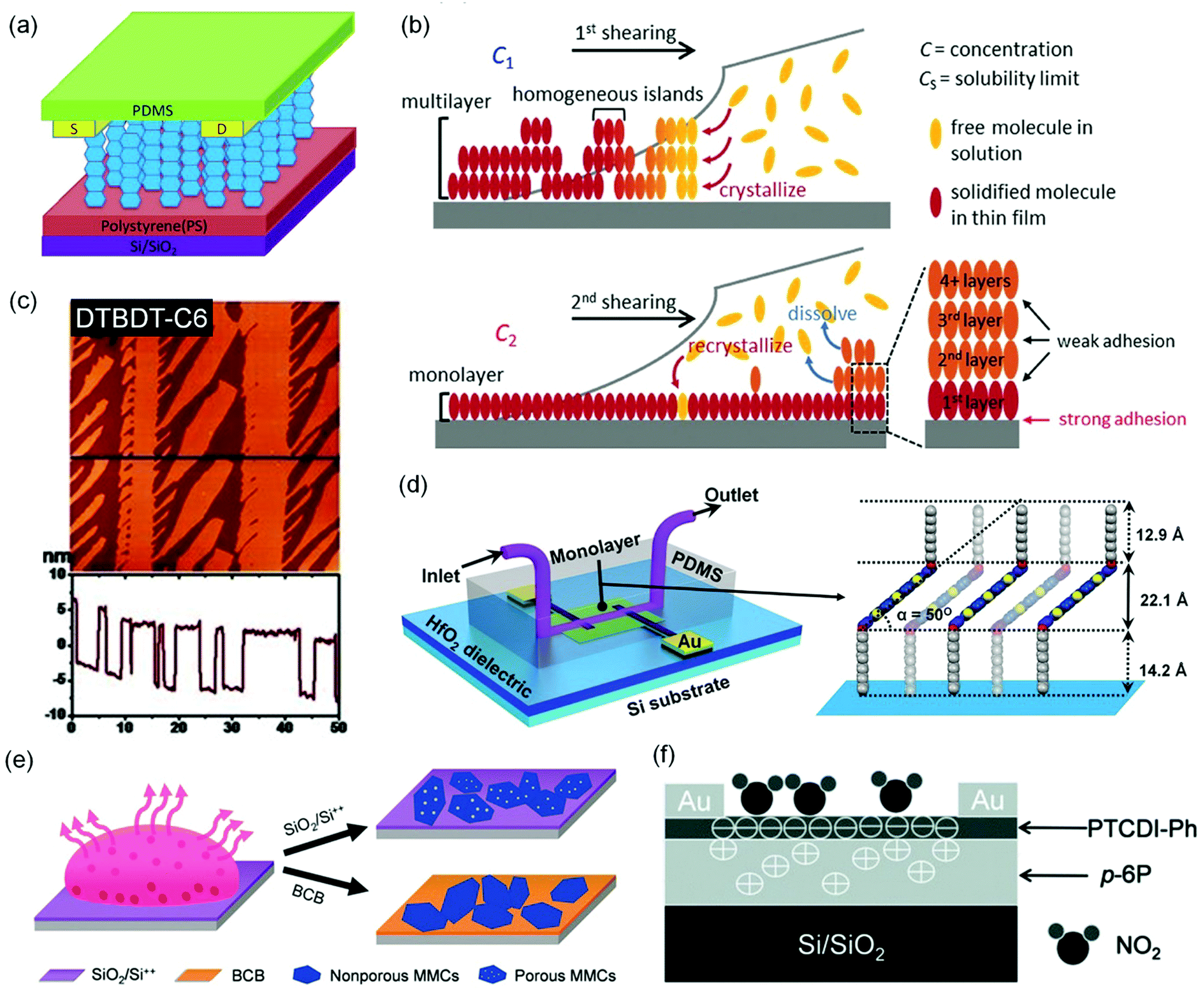 | ||
| Fig. 5 OFET-based sensors with ultrathin-film organic semiconductors. (a) Schematic diagram of a monolayer pentacene device. Reproduced with permission from ref. 33. Copyright 2015 Elsevier. (b) Schematic drawing of the dual-solution-shearing process in the growth of a highly crystallized C10-DNTT monolayer. Reproduced with permission from ref. 37. Copyright 2017 Wiley. (c) Atomic force microscopy (AFM) image and section profile along the line of ultrathin dendritic DTBDT-C6 microstripes. Reproduced with permission from ref. 38. Copyright 2013 Wiley. (d) Schematic of an MFET with a microfluidic channel for real-time detection and a schematic interpretation of a 2R5T2R monolayer on the HfO2 surface, illustrating the three-layer packing model in the monolayer. Reproduced with permission from ref. 39. Copyright 2015 Wiley. (e) Schematic drawing of the preparation of porous NDI3HU-DTYM2 monolayer crystals. Reproduced with permission from ref. 40. Copyright 2020 Wiley. (f) The configuration and sensing model of the heterojunction of PTCDI-Ph and p-6P. Reproduced with permission from ref. 42. Copyright 2013 Wiley. | ||
In comparison to vacuum deposition, solution-based processing methods have been demonstrated to offer ultrathin films of organic semiconductors with higher quality and better control of micro- or nanostructures for chemical sensors.36 Chan and coworkers developed a dual-solution-shearing method (Fig. 5b) to fabricate monolayer crystals of 2,9-didecyldinaphtho[2,3-b:2′,3′-f]thieno[3,2-b]thiophene (C10-DNTT as shown in Fig. 2) with a field effect mobility of up to 10.4 cm2 V−1 s−1, which is favorable for maximizing the current sensitivity caused by trace amounts of analytes.37 As a result, this monolayer OFET of C10-DNTT could sense ammonia in gas with a detection limit as low as 0.01 ppm, and exhibited a relative sensitivity of 850% ppm−1 and 172% ppm−1 in response to 0.1 ppm and 0.01 ppm NH3, respectively. This performance is comparable to that of the vacuum-deposited porous films of DNTT.24 Using a dip-coating method, Chi and coworkers grew dendritic microstripes of dihexyltetrathiapentacene (DTBDT-C6 as shown in Fig. 2) of four to six molecular layers thick and one-dimensional continuity (Fig. 5c).38 In the OFET-based sensors, these microstripes of DTBDT-C6 provided a fast absorption/diffusion path for analyte gas through the surface and intervals between microstripes without compromising efficient charge transport. This sensor exhibited good selectivity for NH3 over a few organic vapors, a detection limit of 10 ppm, a relative sensitivity of 2% ppm−1 in response to 50 ppm NH3, and a fast response/recovery rate. Guo and coworkers fabricated monolayers of bis(3,5-didodecyloxy-phenyl)pentathiophene (2R5T2R as shown in Fig. 2) by optimizing the spin speed and concentration of the solution in a spin coating process. The monolayer OFET of 2R5T2R, in combination with a microfluidic channel, enabled a chemical sensor for melamine in aqueous solution with a detection limit as low as 0.01 ppm (Fig. 5d).39 Most recently, Jiang and coworkers fabricated porous monolayer crystals (Fig. 5e) of NDI3HU-DTYM2 (Fig. 2), an n-type organic semiconductor, by tuning the concentration of NDI3HU-DTYM2 and varying the substrates in the drop-casting process.40 These porous monolayer crystals enabled OFET-based sensors for NH3 in gas with a record low detection limit of 0.1 ppb and relative sensitivity of 720% ppb−1 owing to the unique combination of nanopores and the monolayer structure. In contrast, the non-porous monolayer OFETs exhibited a relative sensitivity of 73% ppb−1 in response to 1 ppb NH3, and the multilayer OFETs only exhibited a relative sensitivity of 0.18% ppm−1 in response to 10 ppm NH3. Moreover, this porous monolayer OFET was able to detect solid dopamine (0.5 ppm) that was diluted with silica powders with a relative sensitivity of 1516% ppm−1.
Monolayer OFET-based sensors can also be formed from organic semiconductor molecules that are equipped with functional groups to react with the dielectric surface. Nuckolls and coworkers reported that acyl chloride-functionalized hexa-cata-hexabenzocoronene (HBC-COCl as shown in Fig. 2) formed a monolayer by forming covalent bonds with the SiO2 surface.41 The monolayer of HBC-COCl, when contacted with nanogap single wall carbon nanotube electrodes, enabled OFET-based sensors that can be immersed into a solution of analyte. This sensor exhibited an increase of the drain current in the output I–V curves by a factor of about 5 in response to 1 mM tetracyanoquinodimethane (TCNQ), a typical electron acceptor, in CH2Cl2.
Heterojunctions
Heterojunctions between different organic semiconductors offer an alternative way to enhance the interactions between analyte molecules in the gas phase and the organic semiconductor layer in an OFET because charge transfer between different organic semiconductors can induce formation of a partially charged surface and accumulation of charge carriers.21 Yan and coworkers fabricated a highly ordered ultrathin film heterojunction by vacuum-deposition of 1 nm of N,N′-diphenylperylene-tetracarboxylic-diimide (PTCDI-Ph as shown in Fig. 2), an n-type semiconductor, on top of 5 nm of para-sexiphenyl (p-6P as shown in Fig. 2), a p-type semiconductor.42 The OFET containing this heterojunction (Fig. 5f) as an active component exhibited a relative sensitivity of 4.9% ppm−1 in response to 5 ppm NO2. In contrast, the single-component OFET of either p-6P or PTCDI-Ph (5 nm thick) in the control experiments was not sensitive to NO2, indicating the crucial role of the heterojunction. Therefore, the sensitivity of this heterojunction device is attributed to charge transfer, which results in larger electron density in the PTCDI-Ph layer, allowing NO2, a strong oxidant, to easily capture electrons. On the other hand, control experiments on a heterojunction with thicker semiconductor layers were not reported in this study. Further deposition of vanadyl phthalocyanine (VOPc), another p-type organic semiconductor, on top of PTCDI-Ph resulted in a double heterojunction, which exhibited a relative sensitivity of 18% ppm−1 in response to 5 ppm NO2 with a fast response and recovery. Using the same strategy, Yan and coworkers also fabricated a heterojunction containing 1.8 nm of titanyl phthalocyanine (TiOPc as shown in Fig. 2), a p-type semiconductor, as the bottom layer and 1 nm of hexadecafluorinated copper phthalocyanine (F16CuPc as shown in Fig. 2), an n-type semiconductor, as the top layer.43 The OFET of this heterojunction exhibited a relative sensitivity of 478% ppm−1 in response to 2 ppm NO2 and a detection limit for NO2 down to 250 ppb.Functionalized organic semiconductors
Although rationally designed physical structures in unfunctionalized organic semiconductors, which lack particular functional groups to interact with target analyte molecules, have enabled highly sensitive detection of NH3 and NO2 in the gas phase with a detection limit down to sub-ppb and sub-ppm levels, respectively, analytes that can be selectively detected by these unfunctionalized organic semiconductors are very limited as shown in Table 1. Selective detection of a broader range of analytes with OFET-based sensors requires functionalized organic semiconductors that are equipped with molecular recognition units or chemical reaction sites to specifically interact with target analytes through non-covalent forces or chemical reactions, respectively. It is worth noting that some organic semiconductors already contain functional groups, such as carbonyl and pyrazine, as indispensable parts of their conjugated backbones, and these functional groups can interact with certain analyte molecules, for example, through hydrogen bonds. However, these backbone functional groups typically cannot enable highly selective recognition. As a result, OFET-based sensors that rely on the backbone functional groups to recognize analyte molecules have rarely been reported.44 The following section is organized according to the method of functionalization of organic semiconductors, namely, physical functionalization and chemical functionalization.Physically functionalized organic semiconductors
A physically functionalized organic semiconductor consists of a semiconductor component and a receptor component, which are not linked together through covalent bonds. The receptor component here is any chemical species that has a recognition unit or a reaction site to interact with the target analyte. Two types of structures, namely, blend and bilayer films, are commonly utilized to combine a receptor and an organic semiconductor together.45Blend films
Studies on a blend of an organic semiconductor and a receptor for chemical sensing have been pioneered by the research group of Katz, who fabricated a blend film by co-evaporating a phthalocyanine semiconductor (CuPc or CoPc) and tris-(pentafluorophenyl)borane (TPFB in Fig. 6b), a receptor that specifically interacts with NH3 through hydrogen bonds and B–N interactions.46 The blend films of CuPc + TPFB and CoPc + TPFB showed lower mobilities and required higher gate voltages for turn-on than the OFETs of CuPc and CoPc, respectively. Upon exposure to 4.5 ppm NH3 for 30 minutes, the drain current of the OFET of CoPc + TPFB decreased by 37%, which is more than three times that of pure CoPc. The OFETs of CoPc + TPFB and CuPc + TPFB exhibited a relative sensitivity of 62% ppm−1 and 58% ppm−1, respectively, in response to 0.45 ppm NH3, and good selectivity for NH3 over methanol, acetone, dichloromethane, ethyl acetate and H2, but poor selectivity over primary amines and H2S. Using a similar strategy, Katz and coworkers developed a sensor for 2,4,6-trinitrotoluene (TNT), a typical explosive, based on the OFET of a solution-processed blend film of poly(3,3′′′-didodecylquaterthiophene) (PQT12 as shown in Fig. 6a) and tetrakis(pentylthio)-tetrathiafulvalene (TPT-TTF as shown in Fig. 6b).47 The PQT12:10% TPT-TTF blend film responded to exposure to 10−4 mg mL−1 TNT in isopropanol with the current increased by about a factor of 8. The increase in current after interaction with TNT is likely due to the formation of a type of complex between TNT and TPT-TTF, which inhibits the trap-induced current decrease caused by TPT-TTF, and dominates the general dipole-trapping caused by TNT in pure PQT12. In contrast, the OFET of pure PQT12 showed a decrease in the drain current on exposure to TNT, probably due to the local fields around analyte dipoles causing charge trapping at grain boundaries. The receptors used in physically functionalized organic semiconductors are not limited to organic compounds but can also be inorganic nanoparticles. In order to solve the highly challenging problem of ethylene (C2H4) sensing, Katz and coworkers developed a sensor based on a blend film consisting of poly(3-hexylthiophene-2,5-diyl) (P3HT as shown in Fig. 6a) as a semiconductor, N-(tert-butoxycarbonyloxy)-phthalimide as an additive to increase the porosity of the P3HT, and palladium (<1 μm diameter) particles as receptors for ethylene molecules because ethylene has an affinity to bind with transition metals.48 With 50 wt% palladium particles, the sensor exhibited a relative sensitivity of 1.2% ppm−1 in response to 25 ppm ethylene. This sensitivity is about 2 times higher than that of the OFET of pure P3HT.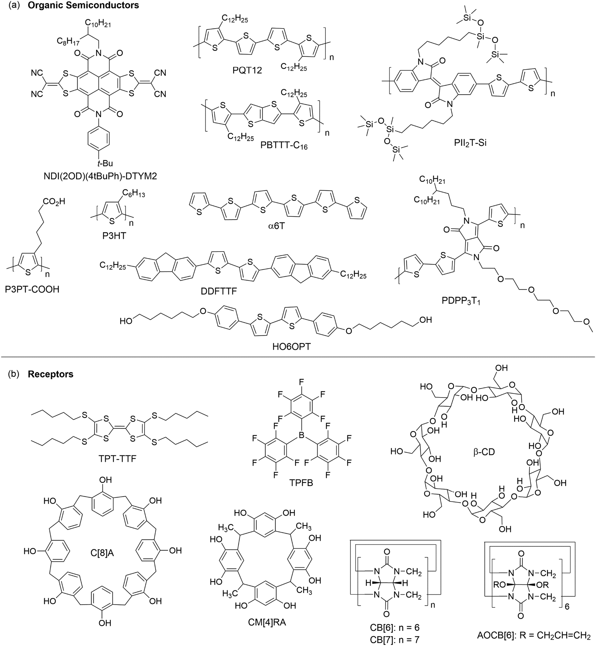 | ||
| Fig. 6 Structures of (a) organic semiconductors and (b) receptors. | ||
Bilayer films
A disadvantage of blending semiconductor and receptor components for OFET-based sensors is that the receptors usually decrease the drain current by impairing charge transport pathways or behaving as traps for charge. To avoid this problem, an alternative way is to deposit a layer of receptors on top of organic semiconductors. As shown in Fig. 6b, classical molecular hosts including calixarene, resorcinarene, cucurbituril and cyclodextrin, which have well defined cavities to accommodate molecular guests, have been used in bilayer structures to physically functionalize organic semiconductors. Bao and coworkers first demonstrated that modification of the surface of a 10 nm-thick film 5,5′-bis-(7-dodecyl-9H-fluoren-2-yl)-2,2′-bithiophene (DDFTTF as shown in Fig. 6a) with a 2 nm-thick layer of calix[8]arene (C[8]A as shown in Fig. 6b) or C-methylcalix[4]-resorcinarene (CM[4]RA as shown in Fig. 6b) resulted in an increase in sensitivity toward ethyl acetate or isopropanol, respectively.49 Kim, Oh and coworkers developed solvent-resistant OFETs based on azide-functionalized P3HT co-polymers, where the azide functional groups enabled photo-cross-linking for stabilization without a loss of electrical performance, and modified the surface of the cross-linked organic semiconductor with a 3 nm layer of C[8]A (Fig. 6b).50 This C[8]A-functionalized OFET was able to detect methanol, ethanol, and n-hexane from solution in toluene with a detection limit of about 1 vol%. In contrast, the OFET without C[8]A showed a detection limit of about 4 vol% with a lower signal intensity. In the same year, Hwang, Kim, Oh and coworkers developed another OFET-based sensor, which had a cucurbit[6]uril derivative, perallyloxyCB[6] (AOCB[6] as shown in Fig. 6b), solution-deposited as a selective sensing layer onto DDFTTF, a water-stable p-type organic semiconductor.51 This sensor enabled detection of acetylcholine (ACh+), a neurotransmitter, in aqueous solution with a detection limit down to 1 × 10⁻¹² M, which is six orders of magnitude lower than that of ion-selective electrode-based sensors. This sensor also showed high selectivity for ACh+ over choline (Ch+) because AOCB[6] binds ACh+ more strongly than Ch+ with an association energy of 86.5 kcal mol−1 and 69.5 kcal mol−1, respectively. More recently, the same research group modified the surface of a layer of DDFTTF with a spin-coated layer of a cucurbit[7]uril (CB[7] as shown in Fig. 6b) derivative, which can selectively bind amphetamine type stimulants.52 This sensor enabled detection of amphetamine hydrochloride and methamphetamine hydrochloride in deionized water, buffer solution and urine with a detection limit down to 1 × 10⁻¹² M. Wang, Xiao and coworkers developed an OFET-based sensor by modifying the surface of a vacuum-deposited film of F16CuPc with a solution-processed layer of β-cyclodextrin (β-CD as shown in Fig. 6b), which is a chiral molecular host.53 This sensor was able to differentiate two enantiomers of a few compounds (phenylalanine, phenyllactic acid, 2-phenylpropanoic acid, mandelic acid, tartaric acid, 2-chloromandelic acid, chiro inositol, and 1,1,2-triphenyl-1,2-ethanediol) in aqueous solution at a concentration of 10−9 M. This capability of chiral differentiation was attributed to different β-CD/enantiomer complex geometries, which resulted in different induced surface polarizations.Ammonia and ammines are also used to modify the surface of organic semiconductors. Zhu and coworkers introduced a receptor layer of absorbed NH3 on the conductive channel of NDI(2OD)(4tBuPh)-DTYM2 (Fig. 6a), an n-type organic semiconductor, by exposing the semiconductor film to 1000 ppm NH3 for a few seconds.54 This NH3-functionalized n-type semiconductor responded to 10 ppm HCl with a relative sensitivity of 3.4% ppm−1 as a result of the reaction between HCl and the absorbed NH3 on the surface of NDI(2OD)(4tBuPh)-DTYM2, leading to the formation of NH4Cl nanoparticles and reduced NH3 doping of the semiconductor. This OFET-based sensor exhibited very good reproducibility in 10 successive cycles of exposure to high concentrations of NH3 and HCl. Unsurprisingly, this OFET-based sensor exhibited very good selectivity for HCl over a variety of volatile organics (isopropanol, chloroform, acetone, o-dichlorobenzene, and hexane), H2S, and SO2, which don’t react with NH3. Interestingly, this sensor was also able to easily differentiate HCl and HBr because no obvious changes in current were observed when the device was exposed to 10 ppm HBr. This difference was attributed to weaker chemical interactions between the adsorbed NH3 and HBr of low concentration based on the fact that no NH4Br nanoparticles were found by AFM when 10 ppm HBr was introduced onto the surface of the NH3-functionalized NDI(2OD)(4tBuPh)-DTYM2 film. Diao and coworkers modified the surface of a nanoporous film of 2,7-dioctyl benzothieno[3,2-b]benzothiophene (C8-BTBT) with a layer of polyethyleneimine, which is rich in primary amine groups to react with formaldehyde. In response to 1 ppb formaldehyde in gas, this functionalized organic semiconductor in OFETs exhibited a relative sensitivity of 5.8% ppb−1, which is higher than that of the device with a non-porous film of C8-BTBT by one order of magnitude.27
Biofunctionalization of semiconductors in an OFET can be enabled by immobilizing biomolecules on the surface of the organic semiconductor layer. Non-covalent biofunctionalization, as discussed below, does not involve formation of covalent bonds to organic semiconductor molecules directly, while biofunctionalization of organic semiconductors through plasma-enhanced chemical vapor deposition (PE-CVD) is discussed in the next section. Gold nanoparticles are used as a medium for biofunctionalization because thiolated biomolecules can be easily immobilized on the gold surface through Au–S bonds. Bao and coworkers modified the surface of a vacuum-deposited semiconductor layer of DDFTTF (Fig. 6a) with an ordered array of gold nanoparticles, which was cast from a self-assembled poly(styrene-b-2-vinylpryidine) matrix, and functionalized the gold nanoparticles with a thiolated DNA aptamer that demonstrated high affinity for thrombin (a protein).55 These biofunctionalized gold nanoparticles enabled the OFET of DDTTTF to detect thrombin in buffer solution with a detection limit of 1 × 10⁻¹⁰ M and high selectivity over other protease proteins. Using essentially the same fabrication methods, Bao and coworkers developed an OFET-based sensor to detect Hg2+ by modifying PII2T-Si (Fig. 6a), a polyisoindigo-based p-type semiconductor containing siloxane-containing solubilizing chains, with DNA-functionalized gold nanoparticles.56 Because this 33-base thiolated DNA probe demonstrated selective binding with Hg2+, this sensor responded to 1 mM Hg2+ in sea water with a relative sensitivity of about 300% mM−1. Remarkably, the high background concentration of salt in seawater (∼600 mM) had only a little effect on the interaction between Hg2+ and this OFET in comparison with the interaction in deionized water. This allowed a detection limit down to 10 μM, and good selectivity for Hg2+ against Zn2+ and Pb2+ in sea water.
Unlike a conventional OFET, an EGOFET has an electrolyte as its gate dielectric and, as a result, the organic semiconductor layer in an EGOFET is in ionic contact with a gate electrode via an electrolyte. Therefore, receptors that are deposited on top of the organic semiconductor layer in an EGOFET can enable specific interactions with target analytes in the electrolyte, leading to modulation of the drain current. Magliulo and coworkers modified the surface of poly[2,5-bis(3-hexadecyllthiophen-2-yl)thieno[3,2-b]thiophene] (PBTTT-C16 as shown in Fig. 6a) in an EGOFET with a layer of spin-coated UV-crosslinked poly(acrylic acid) and then immobilized phospholipid vesicles (prepared from lecithin and phosphatidyl-ethanolamine) on the poly(acrylic acid) through a reaction between the surface carboxylic acid and the amino-group of phosphatidyl-ethanolamine.57 When the phospholipid vesicle was functionalized with biotin, this EGOFET responded to 1.6 × 10⁻¹⁰ M streptavidin in aqueous buffer solution with an increase in the drain current by about 10% and exhibited high selectivity against bovine serum albumin (BSA) owing to the specific interaction between biotin and streptavidin.
Chemically functionalized organic semiconductors
A unique advantage of OFET-based sensors is that reactive groups or binding sites can be covalently attached to organic semiconductors through organic synthesis to provide specific interactions with chosen analytes. However, introduction of functional groups, particularly those capable of strong supramolecular interactions (e.g. hydrogen bonds), usually changes the arrangement of π-faces in the solid state, thus impairing charge transport. It is important but difficult for covalently tailored organic semiconductors to keep a balance between reasonably high field effect mobility for sufficient current and a variety of functional groups available to interact with target analyte molecules. Instead of tailoring each semiconductor molecule by organic synthesis, an alternative method of chemical functionalization is surface reactions, which allow formation of covalent bonds only to the surface of the organic semiconductor layer in an OFET and keep the underneath semiconductor molecules untouched. In other words, chemical functionalization methods can be grouped depending on whether the covalent modification occurs before or after deposition of organic semiconductors to form OFETs.Functionalization of individual semiconductor molecules through synthesis
Katz and coworkers synthesized 5,5′-bis(4-hydroxyhexyl-oxyphenyl)-2,2′-bithiophene (HO6OPT as shown in Fig. 6a), which is a p-type semiconductor functionalized with hydroxyl groups to interact with dimethyl methylphosphonate (DMMP), a nerve gas stimulant, through hydrogen bonds.58 In comparison to the film of 6PTTP6 (Fig. 2), an unfunctionalized semiconductor with the same conjugated backbone as HO6OPT, the co-evaporated blend film (50 nm thick) of HO6OPT and 6PTTP6 exhibited a one order of magnitude lower drain current. As a result, the best sensing performance was achieved by a two-layer OFET, which contained a 35 nm film of 6PTTP6 at the bottom and a 15 nm mixed film of HO6OPT and 6PTTP6 at the top. This two-layer OFET was able to detect DMMP of a concentration as low as 20 ppm in the gas phase with good selectivity over other organic volatiles that can form hydrogen bonds with hydroxyl groups (2-octanone, butyl butyrate, and acetic acid). This selectivity was attributed to the dipole of DMMP, which can trap mobile charges and significantly diminish the drain current by changing both the threshold voltage and the field effect mobility. As reported by the same research group, the ultrathin (4 nm thick) mixed film of HO6OPT and 6PTTP6 exhibited much higher sensitivity responding to 5 ppm DMMP with a decrease in the field effect mobility by 70%.31 Torsi and coworkers developed OFET-based sensors that can discriminate two enantiomers in the gas phase by introducing chiral recognition sites into organic semiconductors.59 Attachment of L-phenylalanine and per-acetylated β-D-glucose groups to a phenylene–thiophene oligomer through covalent bonds resulted in PTA and PTG (Fig. 7a), respectively, and the OFET consisted of a top layer of PTA or PTG and a bottom layer of unfunctionalized phenylene–thiophene oligomer (PTO) to keep a reasonably high field effect mobility. As shown in Fig. 7b, the PTA-PTO OFET was able to differentiate the two enantiomers and a racemic mixture of β-citronellol with a concentration of about 10 ppm, and exhibited sensitivity of −0.08 ± 0.01 nA ppm−1 for (S)-(−)-β-citronellol and −0.04 ± 0.01 nA ppm−1 for (R)-(+)-β-citronellol. As shown in Fig. 7c, the PTG–PTO OFET was able to differentiate two enantiomers of carvone, and exhibited a sensitivity of −0.16 ± 0.01 nA ppm−1 for (S)-(+)-carvone and −0.21 ± 0.01 nA ppm−1 for (R)-(−)-carvone.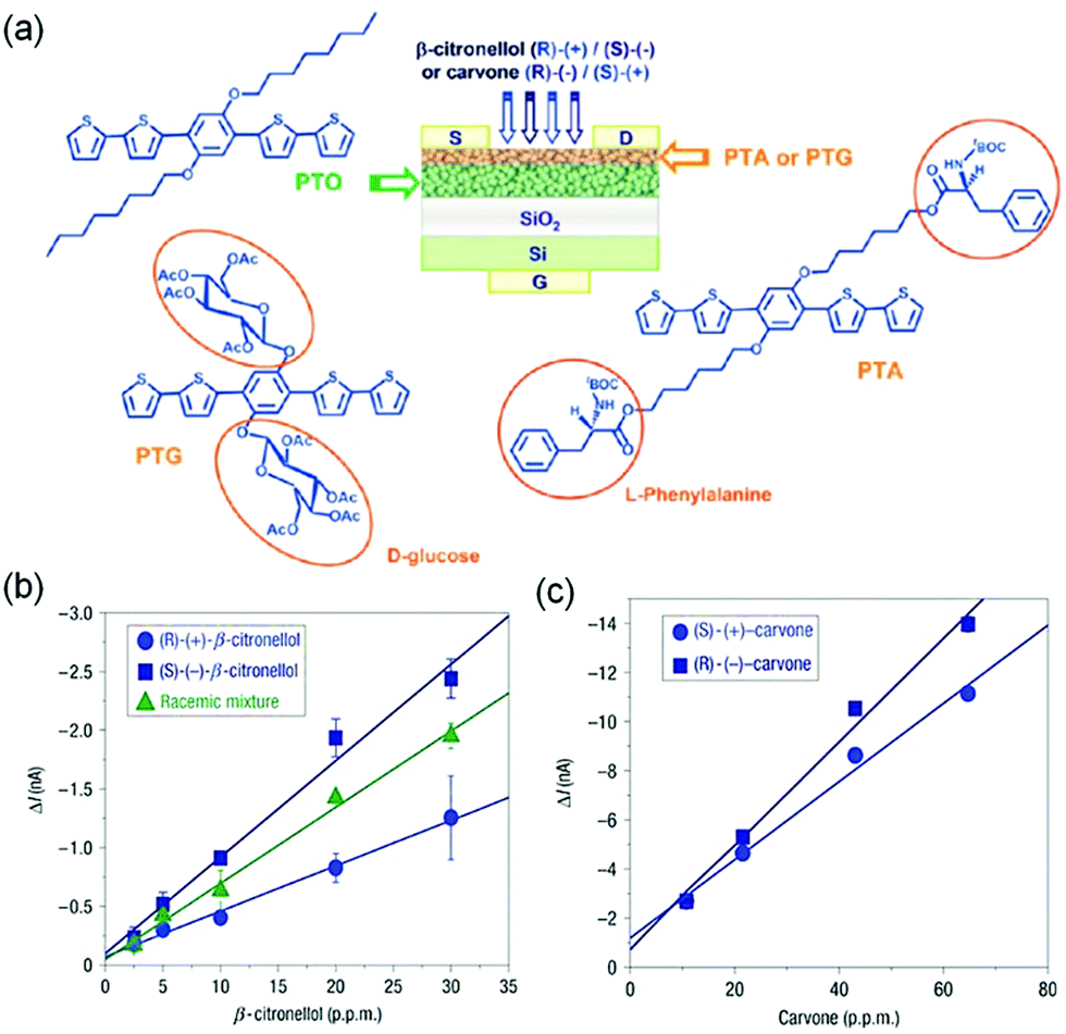 | ||
| Fig. 7 (a) Scheme of the bilayer OFET chiral sensor and the molecular structures of the involved achiral (PTO) and chiral (PTA and PTG) oligomers; (b) the response of the chiral bilayer transistor towards (S)-(–)-β-citronellol, (R)-(+)-β-citronellol, and their racemic mixture as a function of analyte concentration; and (c) the response of the chiral bilayer transistor towards (S)-(+)-carvone and (R)-(−)-carvone. Reproduced with permission from ref. 59. Copyright 2008 Nature Publishing Group. | ||
Functional groups are also attached to conjugated polymers to interact with target analytes. Zhang and coworkers designed and synthesized conjugate polymer PDPP3T1 (Fig. 6a), which has tetraethylene glycol (TEG) chains attached to the poly(diketopyrrolopyrrole-terthiophene) backbone. It was demonstrated that the TEG chain not only facilitated formation of a monolayer at the air–water interface, but also enabled selective detection of alcohol vapors.60 The OFET based on a monolayer of PDPP3T1 responded to 10 ppb alcohols (isopropanol, ethanol or methanol) in the gas phase with a relative sensitivity over 2% ppb−1, and was able to detect ethanol of concentration down to 1 ppb with good selectivity for alcohols over other gas molecules (CO2, hexane, CH2Cl2, acetone, and ethyl acetate), presumably due to the stronger interactions between TEG and alcohols through hydrogen bonds. Attachment of thermally reactive tert-butoxycarboxyl groups to the same poly(diketopyrrolopyrrole-terthiophene) backbone results in pDPPBu-BT (Fig. 8a), which was synthesized by Zhang and coworkers.61 Thermal annealing of a spin-coated film of pDPPBu-BT at 240 °C resulted in a porous film of pDPPCOOH-BT (Fig. 8a) because thermal cleavage of the tert-butoxycarboxyl groups resulted in carboxylic acid groups and release of isobutene as a gas, which created nanopores in the film. The porous film of pDPPCOOH-BT enabled OFET-based sensors for NH3 and ammines (triethylamine, piperidine, and 1,4-diaminobutane) in the gas phase with high sensitivity and good selectivity over other organic volatiles (CH2Cl2, EtOH, ethyl acetate, hexane, and acetone) and HCl. This sensor responded to 0.1 ppm NH3 with a relative sensitivity of 81% ppm−1, and exhibited a detection limit of 10 ppb for NH3. The high sensitivity and selectivity of this sensor can be attributed to the porous nature of the film and the acid–base reactions between the carboxylic acid groups in the film and NH3 and ammines as found from IR spectra.
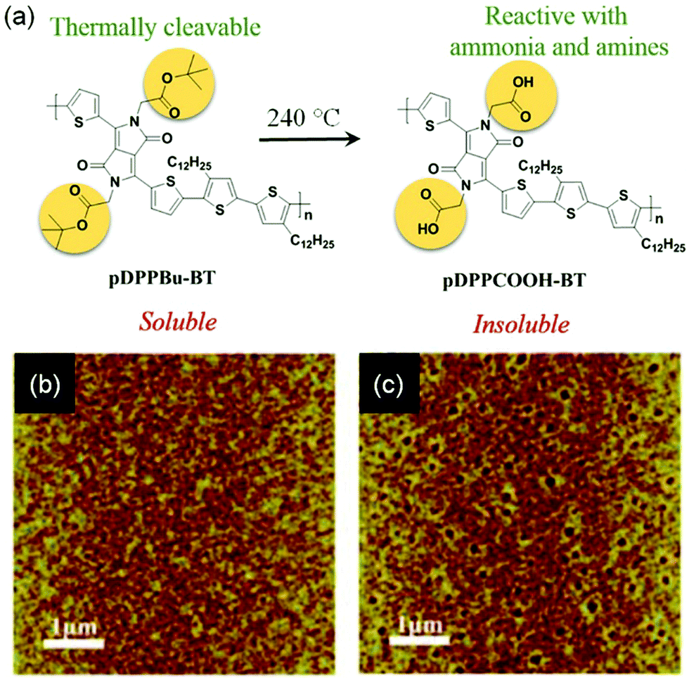 | ||
| Fig. 8 (a) Thermal cleavage of pDPPBu-BT to form pDPPCOOH-BT; (b) AFM image of a thin film of pDPPBu-BT before heating; and (c) AFM image of the same film of pDPPBu-BT after thermal annealing at 240 °C. Reproduced with permission from ref. 61. Copyright 2015 American Chemical Society. | ||
The above functionalized organic semiconductors typically suffer from inefficient charge transport as indicated by the relatively low field effect mobility and even a lack of apparent field effect, presumably because the functional groups impair π–π interactions. How the functional groups affect the π–π interactions of these organic semiconductors remains unclear because the exact molecular packing of the above functionalized organic semiconductors has not been reported. To address this problem, Miao and coworkers recently demonstrated that a series of functional hexabenzoperylenes (HBPs) including HBP–CH3, HBP–COOCH3, HBP–OH and HBP–Cl (Fig. 9a) in the crystal structures exhibit an unusual type of π-stacking,62 which allows a variety of functional groups to be grafted onto organic semiconductors without sacrificing π–π interactions in the solid state.63 As a double [5]helicene, HBP adopts a twisted geometry as the most stable structure, and the brickwork arrangement of twisted π-faces of HBP in the crystals leads to a nanosheet structure. For example, Fig. 9b shows a nanosheet of HBP-OH in crystals, where hydroxyl groups are placed at the exterior of the nanosheet without changing the π-stacking. As a result, the self-assembly of functionalized HBPs provides a general sensing platform in an OFET-based sensor, which combines an OFET channel and a microfluidic channel as shown in Fig. 9c. When HBP was functionalized with silyl ether (HBP-TMS), this sensor responded to 1 μM KF in water with a relative sensitivity of 8% μM−1 and exhibited very good selectivity for fluoride over a range of anions (hydrogen phosphate, nitrate, sulfate, iodide, bromide and chloride) owing to the highly selective cleavage of Si–O bonds by fluoride anions. When HBP was functionalized with biotin (HBP-biotin), this sensor enabled quantitative detection of streptavidin at a concentration as low as 0.036 nM (3.6 × 10⁻¹¹ M) in phosphate buffer solution with a relative sensitivity of 1055% nM−1 as shown in Fig. 9d. The sensor exhibited good selectivity for streptavidin against BSA, a protein that non-specifically adheres to surfaces with a strong tendency, owing to the specific and strong interactions between biotin and streptavidin. In comparison to HBP-biotin, biotin-functionalized semiconducting polymers were reported to exhibit much lower field effect mobility and to respond to streptavidin or avidin at much higher concentration (10−7 M),64,65 likely as a result of poor π–π interactions. When HBP was functionalized with an active ester (HBP-COONP), this sensor enabled differentiation of tertiary amines from primary and secondary amines because tertiary amines, unlike primary and secondary amines, don’t react with the active ester to give the corresponding amides.66
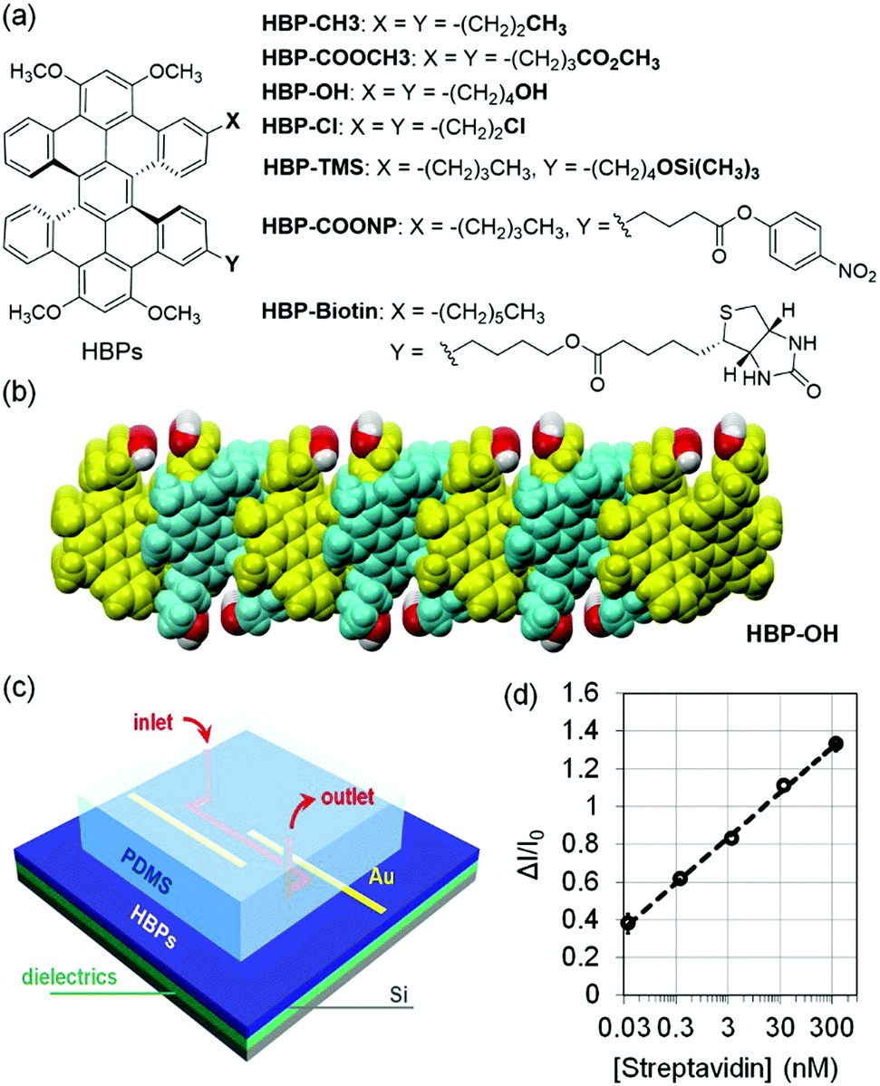 | ||
| Fig. 9 (a) Structure of functionalized HBPs; (b) a nanosheet of HBP-OH in crystals; (c) schematic drawing of the sensor combining a microchannel and a transistor channel of functionalized HBPs; and (d) change of the drain current in the OTFT of HBP-biotin versus the concentration of streptavidin. Reproduced with modification from ref. 63. Copyright 2018 Elsevier. | ||
Postdeposition functionalization through surface chemical reactions
Unlike the strategy of functionalizing individual organic semiconductor molecules as discussed in the above section, the functionalization methods to be discussed in this section involve formation of covalent bonds only to the surface of a deposited organic semiconductor film. As a result, the procedures of surface modification should avoid using solvents that can dissolve the organic semiconductors and harsh conditions that damage the underlying conduction channel. The most widely used method for this purpose is plasma-enhanced chemical vapor deposition (PE-CVD), which is a dry deposition method involving polymerization of organic compounds typically through a free radical mechanism and resulting in covalent bonds between the polymer and the substrate surface.67Bao and coworkers developed an OFET-based sensor by modifying a semiconductor layer of DDFTTF (Fig. 6a) with the following series of surface reactions: (1) deposition of a 5 nm-thick layer of poly(maleic anhydride) by PE-CVD; (2) hydrolysis of the anhydride groups on the polymer surface to carboxylic acid groups in aqueous buffer solution; and (3) attachment of amine-terminated peptide nucleic acid (PNA) strands to the surface by formation of an amide bond with the surface carboxylic acid groups.68 In this process, the 5 nm poly(maleic anhydride) layer provided a contiguous functional layer for further reactions while maintaining a minimal distance between the receptor and the underlying charge transport region. As a result, this sensor was able to detect 100 nM target DNA, which complemented the PNA, with excellent discrimination against single or double base mismatches. In a similar way, Khan et al. used PE-CVD to modify the surface of pentacene with a perfluorinated polymer film for surface passivation and 5 nm thick poly(maleic anhydride) for immobilization of proteins through formation of amide bonds.69 When bovine serum albumin (BSA) was covalently attached to a modified pentacene surface, this sensor was able to selectively detect the corresponding antibody, antiBSA, through the specific antigen/antibody interactions with a detection limit of 10 nM. Torsi and coworkers applied a similar strategy to functionalize the organic semiconductors in EGOFETs with phospholipid vesicles or bilayers, which were covalently linked to PE-CVD deposited polymers on the surface of organic semiconductors. When biotin was covalently linked to the phospholipid vesicles, the EGOFET responded to 1.6 μM streptavidin in buffer solution with a relative sensitivity of 37.5% μM−1, and exhibited a linear relationship between ΔI/I0 and the logarithm of the streptavidin concentration in the range of 10 nM to 1 μM, as a result of the specific biotin/streptavin interaction.70 Treatment of the biotinated phospholipid bilayers with streptavidin and biotinated antibody (anti-CRP) subsequently allowed immobilization of anti-CRP on the surface of organic semiconductors in the EGOFET because streptavidin has four binding sites for biotin. As a result, this EGOFET was able to detect 1 μg mL−1 C-reactive protein (CRP) in serum through the specific antigen/antibody interactions.71
Garrido and coworkers reported an alternative way to modify organic semiconductors in an EGOFET-based sensor including the following series of surface reactions: (1) oxidation of the surface of a layer of α-sexithiophene (α6T as shown in Fig. 6a) by oxygen gas in the presence of UV irradiation to introduce oxygen-related species at the surface; (2) exposure of the oxidized surface to fumes of (3-aminopropyl)triethoxysilane (APTES) to allow formation of Si–O bonds between APTES and oxidized α6T; (3) reaction of the surface amino groups with succinic anhydride to change the surface functionality to carboxylic acid groups; and (4) attachment of penicillinase, an enzyme, to the surface through formation of amide bonds with the carboxylic acids.72 This EGOFET-based sensor was able to detect penicillin in aqueous buffer solution with a detection limit of about 5 μM.
A unique example of postdeposition functionalization of organic semiconductors was reported by Pham and coworkers, who combined postdeposition modification with individually functionalized semiconductor molecules.73 This strategy involved P3PT-COOH (Fig. 6a), a carboxylic acid-functionalized polythiophene, as the organic semiconductor. Oligodeoxynucleotides, as a DNA probe, were grafted to the surface of a spin-coated film of P3PT-COOH through formation of amide bonds between the carboxylic acid group and the amino group in the oligodeoxynucleotide. The EGOFET containing this DNA probe-functionalized semiconductor film responded to hybridization with the complementary target DNA in pure water (not phosphate buffer solution) with a decrease in the off current.
Summary and outlook
As discussed above, structured and functionalized organic semiconductors have enabled OFET-based chemical/biological sensors with high sensitivity and selectivity. Submicrometer-sized pores and ultrathin films have been demonstrated as the most effective physical structures for organic semiconductors to enhance the sensitivity of OFET-based sensors by providing efficient ways to capture analyte molecules from the environment into the conduction channel. Introduction of molecular recognition units or chemical reaction sites into organic semiconductors allows detection of a much broader range of analytes in a more selective manner. However, it has been rarely demonstrated that the sensitivity of functionalized organic semiconductors can be further enhanced by introduction of rationally designed micrometer or nanometer-sized structures in thin films.Nanostructures or functional groups that are designed to facilitate capture or recognition of target analytes often impair charge transport pathways and thus lead to lower electrical current. Therefore, it is key in the development of OFET-based chemical/biological sensors to keep a good balance between efficient charge transport (reflected by a reasonably high field effect mobility) and capability of capturing analyte molecules. Although HBPs (Fig. 9) were recently demonstrated to be equipped with recognition units and reaction sites without sacrificing π–π interactions in the solid state, the general design principles for such a type of organic semiconductors remain unknown. In order to apply OFET-based sensors to detect a broader range of analytes for more practical and valuable applications, we envision opportunities existing in efforts of exploring new π-stacking motifs for organic semiconductors and new surface chemistry for post-deposition modification of organic semiconductors. In particular, combination of a simply functionalized semiconductor molecule and postdeposition reactions with the simple functional group (e.g. carboxylic acid and amino groups) may allow immobilization of more complicated recognition sites on the surface of organic semiconductors through covalent bonds.
As already discussed above, OFET-based biological sensors usually rely on specific interactions of biomolecules, such as antigen–antibody pairs and complementary DNA strands. However, it is not always necessary or practical to design a specific receptor for every target analyte. Instead, a sensor array consisting of a few OFETs that are functionalized with different receptors can be used as a general sensing platform, which is able to provide a specific response pattern of electrical signals as a fingerprint for each analyte. This concept has already been proved by pioneer studies, which mainly used different unfunctionalized organic semiconductors to form an array of OFETs.74–77 We envision that OFET arrays that integrate organic semiconductors functionalized with different receptors will enable highly sensitive electronic noses and electronic tongues that are integrated with wearable electronics in the near future.
Conflicts of interest
There are no conflicts of interest to declare.Acknowledgements
We are grateful for the support from the Croucher Senior Research Fellowship.References
- T. Someya, A. Dodabalapur, J. Huang, K. C. See and H. E. Katz, Chemical and Physical Sensing by Organic Field-Effect Transistors and Related Devices, Adv. Mater., 2010, 22, 3799 CrossRef CAS PubMed.
- Y. Guo, G. Yu and Y. Liu, Functional Organic Field-Effect Transistors, Adv. Mater., 2010, 22, 4427 CrossRef CAS PubMed.
- C. Di, H. Shen, F. Zhang and D. Zhu, Enabling Multifunctional Organic Transistors with Fine-Tuned Charge Transport, Acc. Chem. Res., 2019, 52, 1113 CrossRef CAS PubMed.
- H. Chen, W. Zhang, M. Li, G. He and X. Guo, Interface Engineering in Organic Field-Effect Transistors: Principles, Applications, and Perspectives, Chem. Rev., 2020, 120, 2879 CrossRef CAS PubMed.
- A. N. Sokolov, B. C.-K. Tee, C. J. Bettinger, J. B.-H. Tok and Z. Bao, Chemical and Engineering Approaches To Enable Organic Field-Effect Transistors for Electronic Skin Applications, Acc. Chem. Res., 2012, 45, 361 CrossRef CAS PubMed.
- T. Someya, Z. Bao and G. G. Malliaras, The rise of plastic bioelectronics, Nature, 2016, 540, 379 CrossRef CAS PubMed.
- M. Y. Lee, H. R. Lee, C. H. Park, S. G. Han and J. H. Oh, Organic Transistor-Based Chemical Sensors for Wearable Bioelectronics, Acc. Chem. Res., 2018, 51, 2829 CrossRef CAS PubMed.
- D. Khodagholy, T. Doublet, P. Quilichini, M. Gurfinkel, P. Leleux, A. Ghestem, E. Ismailova, T. Hervé, S. Sanaur, C. Bernard and G. G. Malliaras, In vivo recordings of brain activity using organic transistors, Nat. Commun., 2013, 4, 1575 CrossRef PubMed.
- W. Shi, Y. Guo and Y. Liu, When Flexible Organic Field-Effect Transistors Meet Biomimetics: A Prospective View of the Internet of Things, Adv. Mater., 2019, 1901493 Search PubMed.
- H. Li, W. Shi, J. Song, H.-J. Jang, J. Dailey, J. Yu and H. E. Katz, Chemical and Biomolecule Sensing with Organic Field-Effect Transistors, Chem. Rev., 2019, 119, 3 CrossRef CAS PubMed.
- G. Tarabella, F. M. Mohammadi, N. Coppede, F. Barbero, S. Iannotta, C. Santato and F. Cicoira, New opportunities for organic electronics and bioelectronics: ions in action, Chem. Sci., 2013, 4, 1395 RSC.
- P. Lin and F. Yan, Organic Thin-Film Transistors for Chemical and Biological Sensing, Adv. Mater., 2012, 24, 34 CrossRef CAS PubMed.
- J. Rivnay, S. Inal, A. Salleo, R. M. Owens, M. Berggren and G. G. Malliaras, Organic electrochemical transistors, Nat. Rev. Mater., 2018, 3, 17086 CrossRef CAS.
- N. Wang, A. Yang, Y. Fu, Y. Li and F. Yan, Functionalized Organic Thin Film Transistors for Biosensing, Acc. Chem. Res., 2019, 52, 277 CrossRef CAS PubMed.
- L. Torsi, M. Magliulo, K. Manoli and G. Palazzo, Organic field-effect transistor sensors: a tutorial review, Chem. Soc. Rev., 2013, 42, 8612 RSC.
- S. G. Surya, H. N. Raval, R. Ahmad, P. Sonar, K. N. Salama and V. R. Rao, Organic field effect transistors (OFETs) in environmental sensing and health monitoring: A review, TrAC, Trends Anal. Chem., 2019, 111, 27 CrossRef CAS.
- R. Song, Z. Wang, X. Zhou, L. Huang and L. Chi, Gas-Sensing Performance and Operation Mechanism of Organic π-Conjugated Materials, ChemPlusChem, 2019, 84, 1222 CrossRef CAS PubMed.
- C. Zhang, P. Chen and W. Hu, Organic field-effect transistor-based gas sensors, Chem. Soc. Rev., 2015, 44, 2087 RSC.
- Y. H. Lee, M. Jang, M. Y. Lee, O. Y. Kweon and J. H. Oh, Flexible Field-Effect Transistor-Type Sensors Based on Conjugated Molecules, Chem, 2017, 3, 724 CAS.
- T. Someya, H. E. Katz, A. Gelperin, A. J. Lovinger and A. Dodabalapur, Vapor sensing with α,ω-dihexylquarterthiophene field-effect transistors: The role of grain boundaries, Appl. Phys. Lett., 2002, 81, 3079 CrossRef CAS.
- L. Torsi, A. J. Lovinger, B. Crone, T. Someya, A. Dodabalapur, H. E. Katz and A. Gelperin, Correlation between Oligothiophene Thin Film Transistor Morphology and Vapor Responses, J. Phys. Chem. B, 2002, 106, 12563 CrossRef CAS.
- J. Locklin and Z. Bao, Effect of morphology on organic thin film transistor sensors, Anal. Bioanal. Chem., 2005, 384, 336 CrossRef PubMed.
- L. Huang, Z. Wang, X. Zhu and L. Chi, Electrical gas sensors based on structured organic ultra-thin films and nanocrystals on solid state substrates, Nanoscale Horiz., 2016, 1, 383 RSC.
- S. H. Yu, J. Cho, K. M. Sim, J. U. Ha and D. S. Chung, Morphology-Driven High-Performance Polymer Transistor-based Ammonia Gas Sensor, ACS Appl. Mater. Interfaces, 2016, 8, 6570 CrossRef CAS PubMed.
- B. Kang, M. Jang, Y. Chung, H. Kim, S. K. Kwak, J. H. Oh and K. Cho, Enhancing 2D growth of organic semiconductor thin films with macroporous structures via a small-molecule heterointerface, Nat. Commun., 2014, 5, 4752 CrossRef CAS PubMed.
- J. Lu, D. Liu, J. Zhou, Y. Chu, Y. Chen, X. Wu and J. Huang, Porous Organic Field-Effect Transistors for Enhanced Chemical Sensing Performances, Adv. Funct. Mater., 2017, 27, 1700018 CrossRef.
- F. Zhang, G. Qu, E. Mohammadi, J. Mei and Y. Diao, Solution-Processed Nanoporous Organic Semiconductor Thin Films: Toward Health and Environmental Monitoring of Volatile Markers, Adv. Funct. Mater., 2017, 27, 1701117 CrossRef.
- Q. Wang, S. Wu, F. Ge, G. Zhang, H. Lu and L. Qiu, Solution-Processed Microporous Semiconductor Films for High-Performance Chemical Sensors, Adv. Mater. Interfaces, 2016, 3, 1600518 CrossRef.
- T. Shaymurat, Q. Tang, Y. Tong, L. Dong and Y. Liu, Gas Dielectric Transistor of CuPc Single Crystalline Nanowire for SO2 Detection Down to Sub-ppm Levels at Room Temperature, Adv. Mater., 2013, 25, 2269 CrossRef CAS PubMed.
- Z. Song, Q. Tang, Y. Tong and Y. Liu, High-Response Identifiable Gas Sensor Based on a Gas-Dielectric ZnPc Nanobelt FET, IEEE Electron Device Lett., 2017, 38, 1586 CAS.
- J. Huang, J. Sun and H. E. Katz, Monolayer-Dimensional 5,5′-Bis(4-hexylphenyl)-2,2′-bithiophene Transistors and Chemically Responsive Heterostructures, Adv. Mater., 2008, 20, 2567 CrossRef CAS.
- W. Hu, Y. Liu, Y. Xu, S. Liu, S. Zhou, D. Zhu, B. Xu, C. Bai and C. Wang, The gas sensitivity of a metal–insulator-semiconductor feld-effect-transistor based on Langmuir-Blodgett films of a new asymmetrically substituted phthalocyanine, Thin Solid Films, 2000, 360, 256 CrossRef CAS.
- M. Mirza, J. Wang, L. Wang, J. He and C. Jiang, Response enhancement mechanism of NO2 gas sensing in ultrathin pentacene field-effect transistors, Org. Electron., 2015, 24, 96 CrossRef CAS.
- R. D. Yang, T. Gredig, C. N. Colesniuc, J. Park, I. K. Schuller, W. C. Trogler and A. C. Kummel, Ultrathin organic transistors for chemical sensing, Appl. Phys. Lett., 2007, 90, 263506 CrossRef.
- Y. Jiang, W. Huang, X. Zhuang, Y. Tang and J. Yu, Thickness modulation on semiconductor towards high performance gas sensors based on organic thin film transistors, Mater. Sci. Eng., B, 2017, 226, 107 CrossRef CAS.
- F. Zhang, C. Di, N. Berdunov, Y. Hu, Y. Hu, X. Gao, Q. Meng, H. Sirringhaus and D. Zhu, Ultrathin Film Organic Transistors: Precise Control of Semiconductor Thickness via Spin-Coating, Adv. Mater., 2013, 25, 1401 CrossRef CAS PubMed.
- B. Peng, S. Huang, Z. Zhou and P. K. L. Chan, Solution-Processed Monolayer Organic Crystals for High-Performance Field-Effect Transistors and Ultrasensitive Gas Sensors, Adv. Funct. Mater., 2017, 27, 1700999 CrossRef.
- L. Li, P. Gao, M. Baumgarten, K. Müllen, N. Lu, H. Fuchs and L. Chi, High Performance Field-Effect Ammonia Sensors Based on a Structured Ultrathin Organic Semiconductor Film, Adv. Mater., 2013, 25, 3419 CrossRef CAS PubMed.
- H. Chen, S. Dong, M. Bai, N. Cheng, H. Wang, M. Li, H. Du, S. Hu, Y. Yang, T. Yang, F. Zhang, L. Gu, S. Meng, S. Hou and X. Guo, Solution-Processable, Low-Voltage, and High-Performance Monolayer Field-Effect Transistors with Aqueous Stability and High Sensitivity, Adv. Mater., 2015, 27, 2113 CrossRef CAS PubMed.
- H. Li, Y. Shi, G. Han, J. Liu, J. Zhang, C. Li, J. Liu, Y. Yi, T. Li, X. Gao, C. Di, J. Huang, Y. Che, D. Wang, W. Hu, Y. Liu and L. Jiang, Monolayer Two-dimensional Molecular Crystals for an Ultrasensitive OFET-based Chemical Sensor, Angew. Chem., Int. Ed., 2020, 59, 4380 CrossRef CAS PubMed.
- X. Guo, M. Myers, S. Xiao, M. Lefenfeld, R. Steiner, G. S. Tulevski, J. Tang, J. Baumert, F. Leibfarth, J. T. Yardley, M. L. Steigerwald, P. Kim and C. Nuckolls, Chemoresponsive monolayer transistors, Proc. Natl. Acad. Sci. U. S. A., 2006, 103, 11452 CrossRef CAS PubMed.
- S. Ji, H. Wang, T. Wang and D. Yan, A High-Performance Room-Temperature NO2 Sensor Based on An Ultrathin Heterojunction Film, Adv. Mater., 2013, 25, 1755 CrossRef CAS PubMed.
- X. Wang, S. Ji, H. Wang and D. Yan, Highly sensitive gas sensor enhanced by tuning the surface potential, Org. Electron., 2011, 12, 2230 CrossRef CAS.
- M. Khatib, T.-P. Huynh, J. J. Sun, T. T. Do, P. Sonar, F. Hinkel, K. Müllen and H. Haick, Organic Transistor Based on Cyclopentadithiophene–Benzothiadiazole Donor–Acceptor Copolymer for the Detection and Discrimination between Multiple Structural Isomers, Adv. Funct. Mater., 2019, 29, 1808188 CrossRef.
- Y. Zang, D. Huang, C. Di and D. Zhu, Device Engineered Organic Transistors for Flexible Sensing Applications, Adv. Mater., 2016, 28, 4549 CrossRef CAS PubMed.
- W. Huang, K. Besar, R. LeCover, A. M. Rule, P. N. Breysse and H. E. Katz, Highly Sensitive NH3 Detection Based on Organic Field-Effect Transistors with Tris(pentafluorophenyl)borane as Receptor, J. Am. Chem. Soc., 2012, 134, 14650 CrossRef CAS PubMed.
- H. Kong, B. J. Jung, J. Sinha and H. E. Katz, Electrical “Turn-On” Response of Poly(3,3′′′-didodecylquaterthiophene) and Electron Donor Blend Transistors to 2,4,6-Trinitrotoluene, Chem. Mater., 2012, 24, 2621 CrossRef CAS.
- K. Besar, J. Dailey and H. E. Katz, Ethylene Detection Based on Organic Field-Effect Transistors With Porogen and Palladium Particle Receptor Enhancements, ACS Appl. Mater. Interfaces, 2017, 9, 1173 CrossRef CAS PubMed.
- A. N. Sokolov, M. E. Roberts, O. B. Johnson, Y. Cao and Z. Bao, Induced Sensitivity and Selectivity in Thin-Film Transistor Sensors via Calixarene Layers, Adv. Mater., 2010, 22, 2349 CrossRef CAS PubMed.
- M. Y. Lee, H. J. Kim, G. Y. Jung, A.-R. Han, S. K. Kwak, B. J. Kim and J. H. Oh, Highly Sensitive and Selective Liquid-Phase Sensors Based on a Solvent-Resistant Organic-Transistor Platform, Adv. Mater., 2015, 27, 1540 CrossRef CAS PubMed.
- M. Jang, H. Kim, S. Lee, H. W. Kim, J. K. Khedkar, Y. M. Rhee, I. Hwang, K. Kim and J. H. Oh, Highly Sensitive and Selective Biosensors Based on Organic Transistors Functionalized with Cucurbit[6]uril Derivatives, Adv. Funct. Mater., 2015, 25, 4882 CrossRef CAS.
- Y. Jang, M. Jang, H. Kim, S. J. Lee, E. Jin, J. Y. Koo, I.-C. Hwang, Y. Kim, Y. H. Ko, I. Hwang, J. H. Oh and K. Kim, Point-of-Use Detection of Amphetamine-Type Stimulants with Host-Molecule-Functionalized Organic Transistors, Chem, 2017, 3, 641 CAS.
- Y. Sun, Y. Wang, Y. Wu, X. Wang, X. Li, S. Wang and Y. Xiao, A Chiral Organic Field-Effect Transistor with a Cyclodextrin Modulated Copper Hexadecafluorophthalocyanine Semiconductive Layer as the Sensing Unit, Anal. Chem., 2018, 90, 9264 CrossRef CAS PubMed.
- Y. Zang, F. Zhang, D. Huang, C. Di, Q. Meng, X. Gao and D. Zhu, Specific and Reproducible Gas Sensors Utilizing Gas-Phase Chemical Reaction on Organic Transistors, Adv. Mater., 2014, 26, 2862 CrossRef CAS PubMed.
- M. L. Hammock, O. Knopfmacher, B. D. Naab, J. B.-H. Tok and Z. Bao, Investigation of Protein Detection Parameters Using Nanofunctionalized Organic Field-Effect Transistors, ACS Nano, 2013, 7, 3970 CrossRef CAS PubMed.
- O. Knopfmacher, M. L. Hammock, A. L. Appleton, G. Schwartz, J. Mei, T. Lei, J. Pei and Z. Bao, Highly stable organic polymer field-effect transistor sensor for selective detection in the marine environment, Nat. Commun., 2014, 5, 2954 CrossRef PubMed.
- M. Y. Mulla, P. Seshadri, L. Torsi, K. Manoli, A. Mallardi, N. Ditaranto, M. V. Santacroce, C. Di Franco, G. Scamarcio and M. Magliulo, UV crosslinked poly(acrylic acid): a simple method to bio-functionalize electrolyte-gated OFET biosensors, J. Mater. Chem. B, 2015, 3, 5049 RSC.
- J. Huang, J. Miragliotta, A. Becknell and H. E. Katz, Hydroxy-Terminated Organic Semiconductor-Based Field-Effect Transistors for Phosphonate Vapor Detection, J. Am. Chem. Soc., 2007, 129, 9366 CrossRef CAS PubMed.
- L. Torsi, G. M. Farinola, F. Marinelli, M. C. Tanese, O. H. Omar, L. Valli, F. Babudri, F. Palmisano, P. G. Zambonin and F. Naso, A sensitivity-enhanced field-effect chiral sensor, Nat. Mater., 2008, 7, 412 CrossRef CAS PubMed.
- S.-F. Yang, X. Zhang, P.-L. Chen, Z.-T. Liu, J.-W. Tian, G.-X. Zhang and D.-Q. Zhang, Diketopyrrolopyrrole-Based Semiconducting Polymer with Both Hydrophobic Alkyl and Hydrophilic Tetraethylene Glycol Chains for Monolayer Transistor and Sensing Application, Adv. Electron. Mater., 2017, 3, 1700120 CrossRef.
- Y. Yang, G. Zhang, H. Luo, J. Yao, Z. Liu and D. Zhang, Highly Sensitive Thin-Film Field-Effect Transistor Sensor for Ammonia with the DPP-Bithiophene Conjugated Polymer Entailing Thermally Cleavable tert-Butoxy Groups in the Side Chains, ACS Appl. Mater. Interfaces, 2016, 8, 3635 CrossRef CAS PubMed.
- L. Shan, D. Liu, H. Li, X. Xu, B. Shan, J.-B. Xu and Q. Miao, Monolayer Field-Effect Transistors of Nonplanar Organic Semiconductors with Brickwork Arrangement, Adv. Mater., 2015, 27, 3418 CrossRef CAS PubMed.
- C. Li, H. Wu, T. Zhang, Y. Liang, B. Zheng, J. Xia, J. Xu and Q. Miao, Functionalized π Stacks of Hexabenzoperylenes as a Platform for Chemical and Biological Sensing, Chem, 2018, 4, 1416 CrossRef CAS PubMed.
- Z.-S. Kim, S. C. Lim, S. H. Kim, Y. S. Yang and D.-H. Hwang, Biotin-Functionalized Semiconducting Polymer in an Organic Field Effect Transistor and Application as a Biosensor, Sensors, 2012, 12, 11238 CrossRef CAS PubMed.
- C. Suspène, B. Piro, S. Reisberg, M.-C. Pham, H. Toss, M. Berggren, A. Yassar and G. Horowitz, Copolythiophene-based water-gated organic field-effect transistors for biosensing, J. Mater. Chem. B, 2013, 1, 2090 RSC.
- C. Li, Y. Wang, T. Zhang, B. Zheng, J. Xu and Q. Miao, Tertiary Amines Differentiated from Primary and Secondary Amines by Active Ester-Functionalized Hexabenzoperylene in Field Effect Transistors, Chem. – Asian J., 2019, 14, 1676 CrossRef CAS PubMed.
- R. Sreenivasan and K. K. Gleason, Overview of Strategies for the CVD of Organic Films and Functional Polymer Layers, Chem. Vap. Deposition, 2009, 15, 77 CrossRef CAS.
- H. U. Khan, M. E. Roberts, O. Johnson, R. Förch, W. Knoll and Z. Bao, In Situ, Label-Free DNA Detection Using Organic Transistor Sensors, Adv. Mater., 2010, 22, 4452 CrossRef CAS PubMed.
- H. U. Khan, J. Jang, J.-J. Kim and W. Knoll, In Situ Antibody Detection and Charge Discrimination Using Aqueous Stable Pentacene Transistor Biosensors, J. Am. Chem. Soc., 2011, 133, 2170 CrossRef CAS PubMed.
- M. Magliulo, A. Mallardi, M. Y. Mulla, S. Cotrone, B. R. Pistillo, P. Favia, I. Vikholm-Lundin, G. Palazzo and L. Torsi, Electrolyte-Gated Organic Field-Effect Transistor Sensors Based on Supported Biotinylated Phospholipid Bilayer, Adv. Mater., 2013, 25, 2090 CrossRef CAS PubMed.
- G. Palazzo, D. De Tullio, M. Magliulo, A. Mallardi, F. Intranuovo, M. Y. Mulla, P. Favia, I. Vikholm-Lundin and L. Torsi, Detection Beyond Debye's Length with an Electrolyte-Gated Organic Field-Effect Transistor, Adv. Mater., 2015, 27, 911 CrossRef CAS PubMed.
- F. Buth, A. Donner, M. Sachsenhauser, M. Stutzmann and J. A. Garrido, Biofunctional Electrolyte-Gated Organic Field-Effect Transistors, Adv. Mater., 2012, 24, 4511 CrossRef CAS PubMed.
- L. Kergoat, B. Piro, M. Berggren, M.-C. Pham, A. Yassar and G. Horowitz, DNA detection with a water-gated organic field-effect transistor, Org. Electron., 2012, 13, 1 CrossRef CAS.
- R. D. Yang, J. Park, C. N. Colesniuc, I. K. Schuller, J. E. Royer, W. C. Trogler and A. C. Kummel, Analyte chemisorption and sensing on n- and p-channel copper phthalocyanine thin-film transistors, J. Chem. Phys., 2009, 130, 164703 CrossRef PubMed.
- W. Huang, J. Sinha, M.-L. Yeh, J. F. M. Hardigree, R. LeCover, K. Besar, A. M. Rule, P. N. Breysse and H. E. Katz, Diverse Organic Field-Effect Transistor Sensor Responses from Two Functionalized Naphthalenetetracarboxylic Diimides and Copper Phthalocyanine Semiconductors Distinguishable Over a Wide Analyte Range, Adv. Funct. Mater., 2013, 23, 4094 CrossRef CAS.
- T. Someya, A. Dodabalapur, A. Gelperin, H. E. Katz and Z. Bao, Integration and Response of Organic Electronics with Aqueous Microfluidics, Langmuir, 2002, 18, 5299 CrossRef CAS.
- B. Li, G. Sauvé, M. C. Iovu, M. Jeffries-EL, R. Zhang, J. Cooper, S. Santhanam, L. Schultz, J. C. Revelli, A. G. Kusne, T. Kowalewski, J. L. Snyder, L. E. Weiss, G. K. Fedder, R. D. McCullough and D. N. Lambeth, Volatile Organic Compound Detection Using Nanostructured Copolymers, Nano Lett., 2006, 6, 1598 CrossRef CAS PubMed.
Footnote |
| † We dedicate this paper to Prof. Fred Wudl on the occasion of his 80th birthday. |
| This journal is © the Partner Organisations 2020 |