
 Open Access Article
 This Open Access Article is licensed under a Creative Commons Attribution-Non Commercial 3.0 Unported Licence
On-surface synthesis of size- and shape-controlled two-dimensional Aun nanoclusters using a flexible fullerene molecular template†
Lu'an
Guo‡
 abc,
Yitao
Wang‡
a,
De-Liang
Bao‡
d,
Hai-Hong
Jia
d,
Zhiming
Wang
b,
Shixuan
Du
*d and
Quanmin
Guo
*a
abc,
Yitao
Wang‡
a,
De-Liang
Bao‡
d,
Hai-Hong
Jia
d,
Zhiming
Wang
b,
Shixuan
Du
*d and
Quanmin
Guo
*a
aSchool of Physics and Astronomy, University of Birmingham, Edgbaston, Birmingham B15 2TT, UK. E-mail: q.guo@bham.ac.uk
bInstitute of Fundamental and Frontier Sciences, University of Electronic Science and Technology of China, Chengdu, 610054, People's Republic of China
cDepartment of Applied Physics, and MOE Key Laboratory for Non-equilibrium Synthesis and Modulation of Condensed Matter, Xi'an Jiaotong University, Xi'an, 710049, People's Republic of China
dInstitute of Physics, Chinese Academy of Sciences, Beijing, 100190, China. E-mail: sxdu@iphy.ac.cn
First published on 2nd October 2020
Abstract
Synthesizing nano-clusters with a well-defined size, shape, and composition is an important and challenging goal in nanotechnology. Here we report the application of a single layer C60 molecule as an effective molecular template for the synthesis of size- and shape-selected two-dimensional gold clusters (Aun) on a graphite substrate. This molecular template facilitates the preferential formation of Au19 clusters with a selectivity as high as 90%. Density-functional-theory (DFT) calculations found an energy minimum associated with C60-stabilized two-dimensional Au19 clusters.
Gold nanoclusters (NCs), with their interesting size-dependent plasmonic and catalytic properties, have become an important class of materials in modern technology.1–6 Accurate size-selection of Au NCs has been achieved via either wet chemical synthesis of ligand-protected clusters4 or vacuum-based mass-selected cluster sources.7 Here we introduce size- and shape-controlled synthesis of planar Aun clusters on a graphite substrate. We use a close-packed layer of C60 on graphite as an active molecular template which is able to organize vacuum-deposited Au atoms into discrete Aun clusters. The assembly process is highly efficient with more than 90% of the deposited Au atoms making up the Aun clusters, and is highly selective towards the formation of Au19.
As the physical dimension of the NCs is reduced, the electron energy levels change from quasi-continuous to discrete. This change of energy structure directly affects the carrier lifetimes.8 The shape of the NCs has an equally important effect on the electronic structure. When it comes to the application of metal clusters as building blocks for devices, the clusters are normally required to be resting on a solid substrate for connecting to other components. The cluster–substrate interaction could be an undesirable effect if the intrinsic properties of the cluster are diluted too much via a strong cluster–substrate coupling. We recently synthesized magic number 2D Aun clusters, with n = 19, 35, 49, and 63, on the Au(111) substrate9,10 where a significant energy level mixing between the Aun cluster and the Au(111) substrate is expected. Here we replace the Au(111) substrate with highly oriented pyrolytic graphite (HOPG) with a view to further extending the work to insulating substrates such as SiO2.
Au atoms interact rather weakly with graphite. Therefore, when Au atoms are deposited onto clean HOPG, they diffuse rapidly to step edges or defect sites where large 3-D Au clusters are formed. To stop Au atoms from moving to steps, we deposit a layer of C60 on HOPG first. We then add Au atoms by in situ physical vapour deposition while the C60 covered HOPG is kept at 100 K. Some of the deposited Au atoms “sink” to the HOPG substrate whilst others “float” on top of the C60 layer. The floating Au atoms are mobile at 100 K giving rise to streaks in STM scan lines. There is also evidence that Au atoms are constantly picked up by the STM tip during imaging. By raising the sample temperature to 150 K, we succeed in transporting the floating atoms to the HOPG substrate where Au atoms assemble into single-atomic-layer-high Aun clusters. Each cluster has a footprint not greater than the area occupied by a single C60 molecule, and is stable up to ∼475 K.
Fig. 1a shows an STM image of the sample with 0.026 monolayers (ML) of Au deposited. The sample, prepared using the protocol described above, has been annealed at 375 K for 30 minutes before imaging at room temperature (RT). In this image, we can see a uniform layer of close-packed C60 on HOPG in the background. The bright features in the image appear after the deposition of Au. Most of the bright features are individual spots randomly distributed in the C60 layer. In the magnified image, Fig. 1b, it can be seen that each bright spot occupies exactly the same position as the C60 molecule. The height profile along line M–N, Fig. 1c, shows that the bright spot is ∼0.27 nm taller than the C60 molecules in the background. A number of relatively large, extra bright spots are observed in Fig. 1a and they are highlighted with squares. These extra bright spots have an apparent height of ∼0.8 nm, and their positions are not correlated with the position of the C60 molecules. They can be swept away easily by the STM tip under normal scanning conditions revealing a perfectly organized C60 array underneath.11 Therefore, we assign the extra bright spots as Au clusters floating on top of the C60 layer and will not discuss these clusters any further. Instead, we will focus on the types of bright spots shown in Fig. 1b. These bright spots cannot be moved by the STM tip and they stay in fixed locations without hopping at RT.
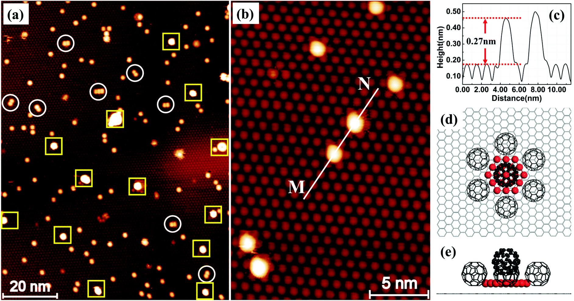 | ||
| Fig. 1 Two-dimensional Aun clusters formed on C60 covered HOPG. (a) STM image of a single C60 layer on HOPG following the deposition of 0.026 ML of Au (sample bias voltage: +1.6 V; tunnel current: 0.1 nA). The sample was kept at 100 K during deposition, and was subsequently annealed in steps to 150 K (30 minutes), 200 K (30 minutes) and 375 K (30 minutes). The image is acquired at RT. The spots with the highest brightness, labelled with squares, are multilayer Au clusters floating on top of the C60 layer. The randomly distributed “bright” C60 molecules in the image are those sitting on 2D Aun islands. (b) Magnified view showing six raised C60 molecules. (c) Height profile measured along line M–N in (b) shows that the bright molecules are ∼0.27 nm taller than the close-packed C60 layer. (d) Top view of the structural model proposed for a (C60)7Au19 cluster. Only C60 molecules associated with the Au cluster are shown for simplicity. Red spheres represent the gold atoms. The C60 molecules are shown, arbitrarily, with one of their hexagonal faces parallel to the HOPG surface. The C60–C60 nearest neighbour distance is 1.0 nm. There is no well-defined single adsorption site for C60 on HOPG. (e) Side view of the structural model. | ||
Based on our observation in the present study and that in an earlier study of the formation of (C60)7Au19 magic number clusters on Au(111),9 we propose a structural model in Fig. 1d and e. According to this model, nineteen Au atoms form a 2D hexagonal island which is surrounded by seven C60 molecules. Six of the seven molecules sit on HOPG next to step edges of the Au island and the seventh molecule sits directly above the Au island. This model provides very good qualitative explanations for the experimental observation. The seven molecules in the (C60)7Au19 cluster keep their preferred close-packing configuration with the nearest neighbor distance of ∼1.0 nm. The C60 molecule sitting on the Au19 island is lifted up by a layer of Au atoms. The size of the Au island (19 atoms) matches the footprint of a single C60 molecule. On the Au(111) surface, each C60 molecule covers an area occupied by twelve Au atoms.12 Here, for the nineteen atom Au island, the edge atoms are shared between two molecules and the corner atom is shared among three C60 molecules, making it 12 atoms per molecule. Analysis of a large number of bright spots shows that the height of the bright spots has a bimodal distribution peaked at 0.27 nm and 0.62 nm (ref. 11) with the majority of the bright spots 0.27 nm tall. We tentatively associate the 0.62 nm height with two-atomic-layer-high Au islands. For example, a two-layer island could be formed with nineteen atoms in the first layer and twelve atoms in the second layer. In Fig. 1a, there are also bright spots appearing in pairs with the distance between the two spots in the pair equal to 1 nm. A number of such pairs are circled in the image. The existence of pairs can be explained as the formation of two edge-sharing hexagons with 35 Au atoms. The edge-sharing hexagons can support two C60 molecules. This is similar to the formation of (C60)10Au35 clusters on Au(111).9
The proposed structural model in Fig. 1d represents the ideal configuration. Only those C60 molecules directly associated with the Au cluster are shown in Fig. 1d for clarity. Adding more atoms to the sides of the island is possible only if one of the C60 molecules is pushed sideways. This creates a barrier against the formation of 2D Au islands consisting of more than nineteen atoms. However, it seems possible to have a 2D gold island with fewer than nineteen Au atoms. For instance, if we remove a single gold atom from one corner of the Au19 island, the remaining structure may still be stable, although not as stable as the Au19 island due to the reduced coordination number and increased step energy. We have evaluated the average number of Au atoms in each cluster by counting the number of clusters within a specified area of the sample and knowing the number of gold atoms contained in that area. From the deposition flux and deposition time, we obtain the number of Au atoms per unit area. We then find an area that does not have the extra bright floating Au clusters. By dividing the total number of Au atoms by the number of “bright” C60 molecules, we find that on average there are ∼18 atoms in each cluster after the sample is annealed at 200 K. This is in good agreement with the proposed nineteen Au atom island considering that there are a small number of two-layer islands with more than 19 atoms. As the annealing temperature is increased to above RT, there is a general trend that the number of clusters decreases with temperature. This may be due to the fragmentation of some clusters with Au atoms released travelling all the way to step edges where large sized Au clusters are formed. For this reason, the estimation of the number of Au atoms per cluster can be performed only for samples that have not been annealed to above RT.
The C60 layer has a 2D lattice that is incommensurate with the HOPG substrate.13 Due to the lack of specific Au–carbon bonds, Au atoms within the 2D island do not occupy a particular site within the graphite lattice. The only conditions required for the formation of the (C60)7Au19 cluster on HOPG are that the seven C60 molecules maintain their preferred intermolecular distance and minimisation of step energy for the nineteen Au atom island.
The formation of 2D Au clusters with size and shape control makes the C60 layer an effective molecular template which can be compared with nanosphere lithography (NSL) or colloidal lithography (CL).14,15 In colloidal lithography, a layer of close-packed colloidal particles is used as a mask. The individual colloidal particles prevent the material reaching to the area of the substrate covered by the particles. Deposition of a material through the interstitial sites of the colloidal monolayer creates a patterned array of the deposited material. By using colloidal particles of different diameters, the size of the deposited features on the substrate can be controlled. The smallest colloidal particles that have been successfully used in NSL are ∼80 nm in diameter. The single layer of C60 on HOPG has all the characteristics of a colloidal lithographic mask with individual C60 molecules behaving as 1 nm sized “colloidal” particles. For conventional NSL, the mask is a passive structure blocking the pathway of incoming atoms at pre-defined locations. The diffusion length of the atom is usually much smaller than the size of the colloidal spheres. What is shown here is that the conventional CL does not scale down to the molecular level where the simple blocking mechanism ceases to operate. There is no proven method for lifting the C60 mask. However, polymerisation of C60 molecules can be achieved and it seems possible that the polymerised C60 layer be lifted together with the trapped Au clusters.
The Au atom does not form a specific chemical bond with the carbon atoms in C60. The Au–C60 bond is formed via charge transfer from Au to C60.16 We expect a similar type of charge transfer from the 2D Au cluster to the C60 molecules. We have not performed any scanning tunnelling spectroscopic (STS) analysis of the molecules within the (C60)7Au19 cluster. However, images obtained at positive and negative sample bias voltages clearly demonstrate the effect of charge transfer. In Fig. 2, we show two STM images acquired from the same area of the sample with different bias voltages. The image in Fig. 2(a) is obtained using +1.80 V. A height profile measured along the red line in (a) is shown in Fig. 2(b). The bright spot as position 1 is 0.87 nm taller than the C60 layer. This is from a 3D Au cluster, ∼3 atomic layers high, which floats on top of C60. Fig. 2(c) shows an STM image obtained at −1.21 V. Under negative sample bias, the (C60)7Au19 cluster stands out more dramatically from the background. In addition to the bright molecule sitting on the Au island, the other six molecules sitting next to the sides of the Au hexagon appear significantly taller than the molecules in the background. This indicates an enhanced charge density of the seven molecules within the (C60)7Au19 cluster. This enhancement can be attributed to charge transfer from the Au cluster making Au–C60 behave as an electrical dipole. Under negative sample bias, electrons flow out of the molecule into the STM tip. Under positive sample bias, the tip injects electrons into the molecule which works against the internal charge flow from Au to C60. A higher conductance is expected for negative bias. The multilayer Au clusters floating on top of the C60 layer also appear taller under negative sample bias. A more detailed investigation by performing STS measurement on each of the seven C60 molecules in the cluster is desirable to obtain more information on the electronic structure of the cluster.
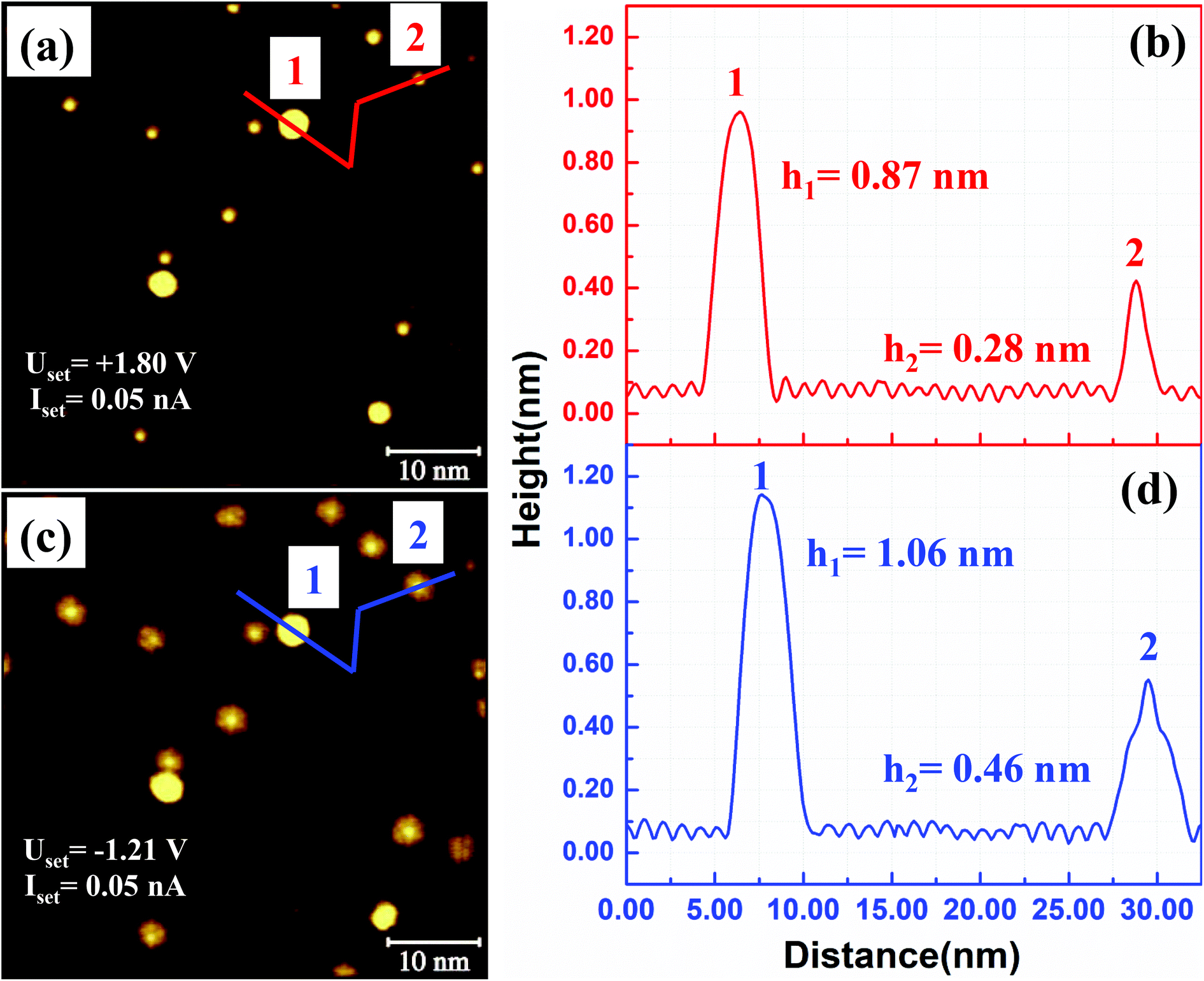 | ||
| Fig. 2 Bias voltage dependent heights of Aun clusters. (a) STM image acquired with a positive sample bias of +1.80 V. (b) Height profile along the red lines. A ∼ three-layer Au cluster is found at position 1. A 2D (C60)7Au19 cluster is located at position 2. (c) The same area imaged with a negative sample bias of −1.21 V. For the (C60)7Au19 clusters, in addition to the molecule sitting on the Au island, the surrounding six molecules appear taller than molecules in the background due to charge transfer from the Au island. (d) Height profile along the blue lines in (c). | ||
STM images provide strong evidence for highly efficient size-selection of Aun clusters. However, the exact number of Au atoms within each cluster cannot be obtained from STM imaging because the Au cluster is sandwiched between C60 and HOPG. We therefore performed density-functional-theory (DFT) calculations.
As shown in Fig. 3a and b, a 12 × 12 graphene/3 × 3 C60 supercell is used in DFT calculations. Neighboring Au clusters are kept apart at about 2 nm, which is large enough to ignore inter-cluster interactions. The structure of the relaxed Au19 cluster, Fig. 3c, shows that the Au atoms on each edge of the hexagon interact strongly with C60 molecules through charge transfer. The charge density difference is obtained by ρ(total) − ρ(Aux = 19) − ρ(C60/graphene) (ρ denotes electron density). From the spatial distribution of the charge density difference shown in Fig. 3c, we find that edge Au atoms donate electrons to the nearest C60 molecules. Fig. 3d and e show the different-sized clusters studied and the adsorption energy per Au atom as a function of cluster size. The adsorption energy is defined as, Eads = [E(C60/Aux/graphene) − E(C60/graphene) − x × E(Au)]/x, where E(C60/Aux/graphene) and E(C60/graphene) are the total energies of C60/Aux/graphene and C60/graphene, respectively. E(Au) is the total energy of a single Au atom. x is the number of Au atoms in the cluster. The minimum energy appears for the cluster with 19 Au atoms. The specific binding energy difference is not much greater than thermal energy at RT. For example, the energy difference between Au18 and Au19 is 0.01 eV. The energy difference per cluster, however, is 0.18 eV which is high enough to steer the selectivity towards the most stable cluster. It is worth mentioning that, when an extra Au is introduced, (the green balls in panels 20 and 20′ in Fig. 3e), it prefers to go up to the second layer (x = 20′) rather than to stay in the first layer (x = 20). This finding agrees with the experimental observation that monolayer and bilayer islands coexist. The structural stability of the Au19 cluster at 300 K is further evaluated using classical-molecular-dynamics (MD) calculations. We find that the Au19 cluster is stable at 300 K. Details of MD findings can be found in Fig. S4 in the ESI.†11 The CIF file for the (C60)7Au19 can be found at the Cambridge Crystallographic Data Centre (CCDC) with deposition number 2034815.†
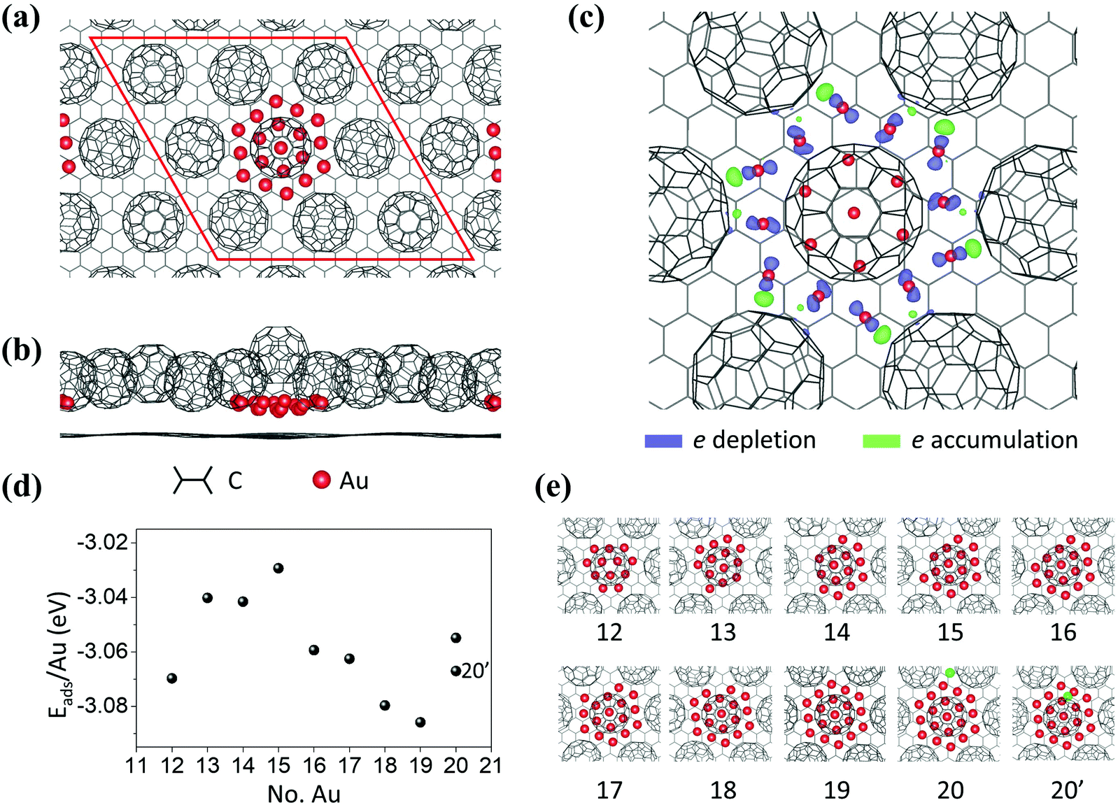 | ||
| Fig. 3 DFT calculations on Aun clusters. (a) Top view and (b) side view of the atomic model in DFT calculations. (c) Charge density difference between Au and C60 molecules. Blue and green shadows represent electron depletion and accumulation, respectively. The isosurface is 0.053 e Å−3. (d) Adsorption energy per Au atom as a function of the number of Au atoms shows a dip corresponding to 19 Au atoms. (e) Top views of the atomic configurations of the different Au clusters considered in the calculations. | ||
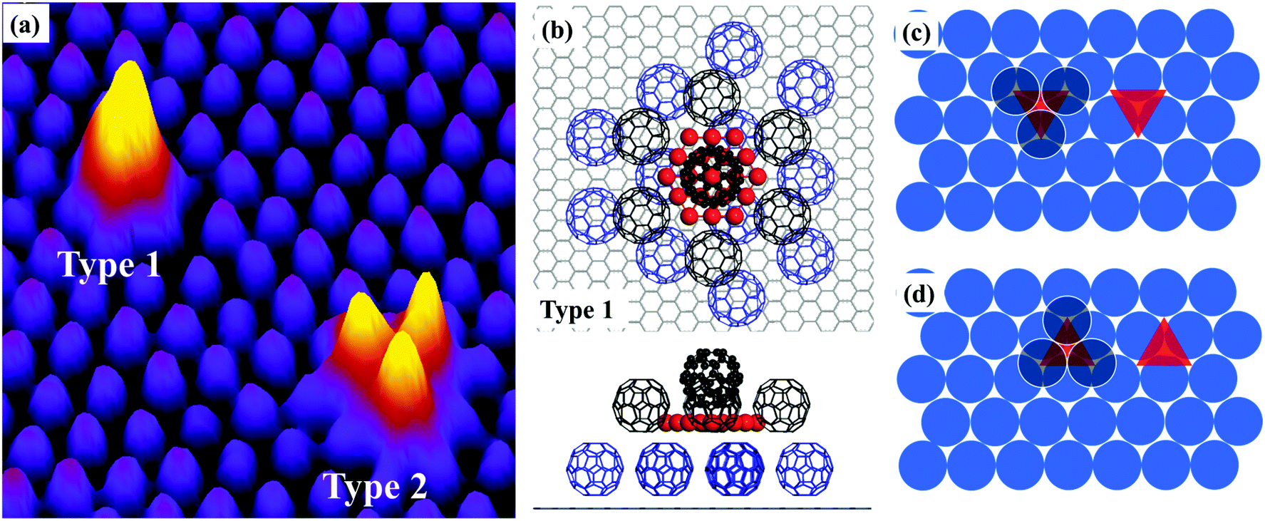
We have also investigated the deposition of Au atoms onto 2 ML C60 on HOPG. Fig. 4(a) shows an STM image of HOPG which is covered by ∼1.5 ML of C60. In the image, there are three second layer C60 islands, I, II and III, sitting on a complete 1st layer. After 0.026 ML of Au is deposited at 100 K and thermal annealing to 200 K for 30 minutes, we observed bright (raised) features in both the first and the second C60 layers. A close examination finds that there are two types of bright spots in the second layer. Type I is singly raised C60 molecules about 0.22 nm taller than the normal molecules. This is similar to the raised molecules found in the first layer. We also find a number of bright C60 trimers, type II, standing 0.17 nm tall from the background. The trimer/monomer number ratio is ∼1![[thin space (1/6-em)]](https://www.rsc.org/images/entities/char_2009.gif) :3. Inset I in Fig. 4(a) is a magnified view taken from island I. The C60 trimer consists of three adjacent C60 molecules and it takes the same azimuthal orientation. Trimers in island II take a uniform orientation which is, however, flipped upside down in comparison to those in island I. Trimers in island III take the same orientation as those in island II.
:3. Inset I in Fig. 4(a) is a magnified view taken from island I. The C60 trimer consists of three adjacent C60 molecules and it takes the same azimuthal orientation. Trimers in island II take a uniform orientation which is, however, flipped upside down in comparison to those in island I. Trimers in island III take the same orientation as those in island II.
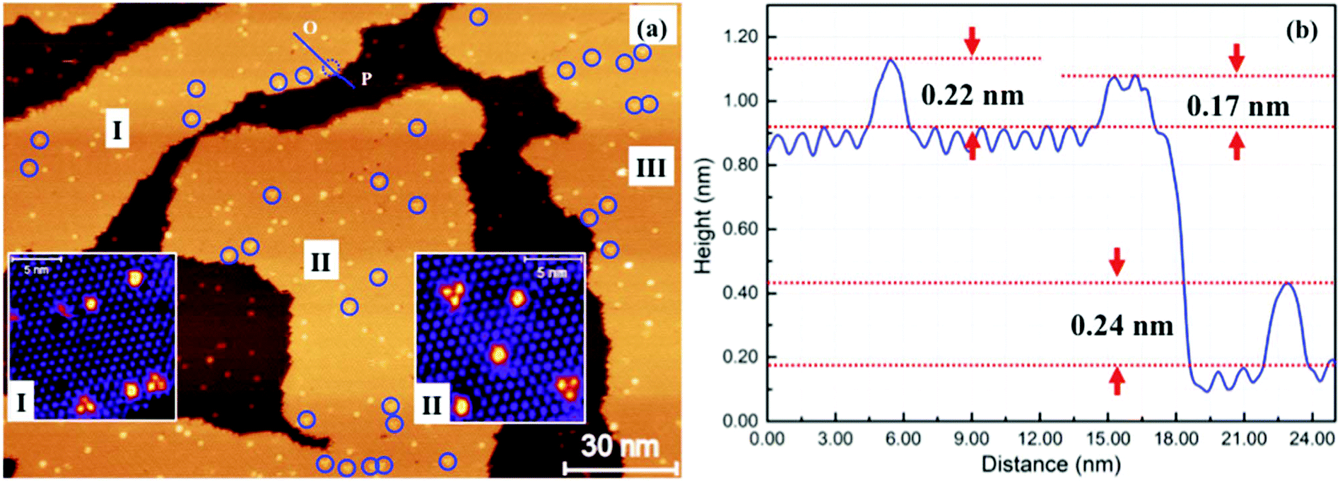 | ||
| Fig. 4 Au clusters sandwiched between two layers of C60. (a) STM image from an area of HOPG covered by ∼1.5 ML of C60. I, II and III are three second layer C60 islands. Bright spots in the second layer are due to the trapping of Au atoms. In addition to singly raised C60 molecules, there are bright C60 “trimers” as shown in inset I which is a magnified view from part of island I. The trimers have the same azimuthal orientation within the same island. Inset II is a magnified view taken from part of island II. The trimer orientation is flipped upside down in comparison to those in I. (b) Height profile measured along line O–P. The single bright C60 in the second layer is 0.22 nm taller than the normal C60 molecule in this layer. The C60 trimer is 0.17 nm tall. | ||
For singly raised C60 in the second layer, we propose a structural model shown in Fig. 5(b). According to this model, there is a Au cluster directly below the raised molecule. The cluster occupies the tetrahedral interstice of the C60 lattice. It is not clear what shape is this cluster. The cluster is larger than the volume of the interstice lifting the C60 above by ∼0.22 nm. A structural model for the raised C60 trimer is presented in Fig. 5(c). Here a Au cluster is placed in the octahedral interstice. If we shift the position of the second layer C60 from the occupied three-fold hollow site shown in Fig. 5(c) to the nearest neighbour three-fold hollow site, the octahedral interstice moves as a result, Fig. 5(d). Therefore, the orientation of the raised trimer in Fig. 5(d) is opposite to that in Fig. 5(c). The orientation of the trimer within one domain should be the same independent of the location. The number density of raised features (trimer plus monomer) in the second layer is not much different from that of the raised monomers in the first layer. If all the Au atoms landing on top of the second layer form trapped clusters between the two layers, the average size of the clusters trapped between the layers should be similar to that of the Au 2D cluster in the first layer, i.e. around 19 Au atoms per cluster. As the sample is annealed progressively to higher temperatures, we find that the number of trimers diminishes whilst the number of singly raised molecules remains relatively constant. This suggests that the Au cluster at the octahedral interstice is less stable. There are nearly three times as many raised C60 monomers as raised trimers. This is probably due to the fact that there are twice as many tetrahedral sites as octahedral sites, assuming an equal probability of nucleation at the two different types of interstice. Nano-structures from the self-assembly of the C60 molecule have been studied previously in the absence of metal atoms.17,18 What we have demonstrated here is that the flexibility of the C60 layer can be effectively used to regulate the formation of Au nanoclusters.
 | ||
| Fig. 5 Structural models of Au clusters trapped between two layers of C60. (a) STM image showing two types of raised features. Type I: a single raised C60 molecule. Type II: a raised C60 trimer. The C60 molecules in this image are all in the second layer. (b) Structural model for Au clusters trapped at the tetrahedral interstitial site. (c) Structural model for Au clusters trapped at the octahedral site. (d) Alternative arrangement of the octahedral site. The raised C60 trimer in (c) has an opposite orientation to that in (d). | ||
In summary, a close-packed layer of C60 on HOPG has been used as an effective molecular template for the fabrication of size- and shape-controlled Au clusters. The interaction between Au and the C60 molecules leads to the preferential formation of the planar Au19 cluster which is protected by seven C60 molecules. The on-surface synthesis of size- and shape-controlled clusters thus developed is potentially useful for making regular two-dimensional cluster lattices. C60 double layers are found to be able to trap small Au clusters in between the layers. Such trapped clusters might be three-dimensional with a lateral dimension less than 1 nm. Small metal clusters sandwiched between organic molecular layers are good candidates for solar energy harvesting and energy storage. Further investigation targeting at the electronic structure of the Au clusters would provide more information on the activity of the clusters and their optical response.
Methods
HOPG (purchased from Goodfellow, 99.99% purity) was used as the substrate. The HOPG sample was prepared by annealing in UHV at 475 K for 30 min to remove surface contamination just before the deposition of the C60 molecules (purchased from MER, 99.5% purity) that were sublimed onto the HOPG substrate using home-built effusion cells. The effusion cells are degassed at 500 K for 5 min before sublimation. Then the C60 molecules were deposited on the surface with a rate of 0.12 ML min−1 for 10 min. During deposition, the background pressure in the UHV system does not exceed 10−9 mbar. After the C60 deposition completed, the sample was cooled down to 100 K with L–N2. Then gold atoms were deposited using a Createc high-temperature effusion cell with a rate of 0.026 ML min−1 for 1 min. After the deposition of gold atoms, the sample was annealed at 150 K (30 minutes) and then at 200 K (30 minutes) before finally warming up to RT. STM imaging was performed with an Omicron UHV VT STM. Electrochemically etched tungsten tips were used after high temperature annealing in the UHV chamber. Images were collected using the constant current mode with the tunnelling current set at 0.1 nA and bias voltage varying from −1.70 V to +2.00 V. Gwyddion19 software was used to analyze the raw data acquired by the Omicron MATRIX 3.3.Density-functional-theory (DFT) calculations were performed using the Vienna ab initio Simulation Package (VASP).20 Perdew–Burke–Ernzerhof (PBE)21 general gradient approximation (GGA)22 and projector augmented wave (PAW)23 pseudo-potentials were employed to treat the exchange–correlation functions and electron–ion interactions. Grimme's D3 correction24 was adopted to describe the van der Waals (vdW) interaction. For geometrical optimization, all the atoms were fully relaxed to reach a force tolerance of 0.02 eV Å−1. The calculation cell contains one layer of 12 × 12 graphene and one layer of 3 × 3 C60 on one side, with an Au cluster in between. The neighboring Au clusters are separated by ∼2 nm. A 17 Å vacuum gap was added to prevent the interaction between slabs. The cut-off energy was 400 eV and the K-point mesh was gamma only.
Molecular dynamics (MD) simulations were carried out under the NVT ensemble with Gromacs-4.6.7 software.25 The supercell contains four layers of 64 × 64 graphene and one layer of 8 × 8 C60 molecules on one side, with two Au19 clusters in between. The general AMBER force field (GAFF) was used to describe intra- and intermolecular interaction parameters of a C60 molecule and graphene.26 Girifalco's parameters are employed to describe vdW interactions for fullerene carbons.27 The Au atoms interacted with each other (or carbon atoms) via the Lennard-Jones (LJ) potential.28 The Berendsen thermostat is applied to control the temperature. A time step of 1 fs is used in all simulations. A typical of 12 Å cut-off distance is used in the calculation of vdW interactions. The simulation process includes three steps. First, the system undergoes a 5 ns simulation at 100 K to obtain an equilibrium configuration. Second, using the final trajectory at 100 K as the initial structure, the system was heated to 375 K with a heating rate of 1 K ps−1, performed a 20 ns simulation at 375 K, and was cooled to 300 K with a cooling rate of 1 K ps−1. Finally, using this final trajectory in the previous step, we carried out a 20 ns simulation at 300 K to check its stability.
Author contributions
Lu'an Guo and Yitao Wang conducted all experiments. De-liang Bao and Hai-hong Jia performed theoretical calculations. All authors contributed to data analysis and writing of the manuscript.Conflicts of interest
The authors declare no competing financial interest.Acknowledgements
We thank the Chinese Scholarship Council for providing a studentship.References
- M. Zhou, T. Higaki, G. Hu, M. Y. Sfeir, Y. Chen, D.-E. Jiang and R. Jin, Three-orders-of-magnitude variation of carrier lifetimes with crystal phase of gold nanoclusters, Science, 2019, 364, 279–282 CrossRef CAS.
- E. C. Tyo and S. Vajda, Ctalysis by clusters with precise number of atoms, Nat. Nanotechnol., 2015, 10, 577588 CrossRef.
- S. Yang, J.-S. Chai, Y.-B. Song, J.-Q. Fan, T. Chen, S.-X. Wang, H.-Z. Yu, X.-W. Li and M.-Z. Zhu, In situ two-phase ligand exchange: A new method for the synthesis of alloy nanoclusters with precise atomic structuires, J. Am. Chem. Soc., 2017, 139, 5668–5671 CrossRef CAS.
- R. Jin, C. J. Zeng, M. Zhou and Y.-X. Chen, Atomically precise colloidal metal nanoclusters and nanoparticles: Fundamentals and opportunities, Chem. Rev., 2016, 116, 10346–10413 CrossRef CAS.
- W. C. D. Yang, C. H. Wang, L. A. Fredin, P. A. Lin, L. Shimomoto, H. J. Lezec and R. Sharma, Site-selective CO disproportionation mediated by localized surface plasmon resonance excited by electron beam, Nat. Mater., 2019, 18, 614–619 CrossRef CAS.
- P. M. Larsen, K. W. Jacobsen and J. Schiotz, Rich ground-state chemical ordering in nanoparticles: Exact solution for AgAu clusters, Phys. Rev. Lett., 2018, 120, 256101 CrossRef CAS.
- D. M. Foster, R. Ferrando and R. E. Palmer, Experimental determination of the energy difference between competing isomers of deposited, size-selected gold nanoclusters, Nat. Commun., 2018, 9, 1323 CrossRef CAS.
- K. Kwak, V. D. Thanthirige, K. Pyo, D. Lee and G. Ramakrishna, Energy gap law for exciton dynamics in gold cluster molecules, J. Phys. Chem. Lett., 2017, 8, 4898–4905 CrossRef CAS.
- Y.-C. Xie, L. Tang and Q. Guo, Coopreative assembly of magic number C60-Au complexes, Phys. Rev. Lett., 2013, 111, 186101 CrossRef.
- D. Kaya, D.-L. Bao, R. E. Palmer, S.-X. Du and Q. Guo, Tip-triggered thermal cascade manipulation of magic number gold-fullerence clusters in the scanning tunneling microscope, Nano Lett., 2017, 17, 6171–6176 CrossRef CAS.
- L. Guo, Y.-T. Wang, D.-L. Bao, H.-H. Jia, Z.-M. Wang, S.-X. Du and Q. Guo, ESI.†.
- E. I. Altman and R. J. Colton, Nucleation, growth, and structure of fullerene films ob Au(111), Surf. Sci., 1992, 279, 49–67 CrossRef CAS.
- H. Shin, S. E. O'Donnell, P. Renke, N. Ferralis, A. K. Schmid, H. I. Li, A. D. Novaco, L. W. Bruch and R. D. Diehl, Floating two-dimensional solid monolayers of C60 on graphite, Phys. Rev. B: Condens. Matter Mater. Phys., 2010, 82, 235427 CrossRef.
- H. W. Deckman and J. H. Dunsmuir, Natural lithography, Appl. Phys. Lett., 1982, 41, 377–379 CrossRef CAS.
- R. Van Dommelen, P. Fanzio and L. Sasso, Surface self-assembly of colloidal crystals for micro- and nano-patterning, Adv. Colloid Interface Sci., 2018, 251, 97–114 CrossRef CAS.
- X. Lu, M. Grobis, K. H. Khoo, S. G. Louie and M. F. Crommie, Charge transfer and screening in individual C60 molecules on metal substrates: A scanning tunneling spectroscopy and theoretical study, Phys. Rev. B: Condens. Matter Mater. Phys., 2004, 70, 115418 CrossRef.
- M. Sathish and K. Miyazawa, Size-tunable hexagonal fullerene (C60) nanosheets at the liquid-liquid interface, J. Am. Chem. Soc., 2007, 129, 13816–13817 CrossRef CAS.
- J. L. de Boer, S. van Smaalen, V. Petricek, M. DusekP, M. A. Verheijen and G. Meijer, Hexagonal close-packed C60, Chem. Phys. Lett., 1994, 219, 469–472 CrossRef CAS.
- D. Nečas and P. Klapetek, Gwyddion: An open-source software for SPM data analysis, Open Phys., 2012, 10, 181–188 Search PubMed.
- D. Vanderbilt, Soft self-consistent pseudopotentials in a generalized eigenvalue formalism, Phys. Rev. B: Condens. Matter Mater. Phys., 1990, 41, 7892–7895 CrossRef.
- J. P. Perdew, K. Burke and M. Ernzerhof, Generalized gradient approximation made simple, Phys. Rev. Lett., 1996, 77, 3865–3868 CrossRef CAS.
- J. P. Perdew, J. A. Chevary, S. H. Vosko, K. A. Jackson, M. R. Pederson, D. J. Singh and C. Fiolhais, Atoms, molecules, solids, and surfaces: applications of the generalized gradient approximation for exchange and correlation, Phys. Rev. B: Condens. Matter Mater. Phys., 1992, 46, 6671–6687 CrossRef CAS.
- G. Kresse and D. Joubert, From ultrasoft pseudopotentials to the projector augmented-wave method, Phys. Rev. B: Condens. Matter Mater. Phys., 1999, 59, 1758–1775 CrossRef CAS.
- S. Grimme, J. Antony, S. Ehrlich and H. Krieg, A consistent and accurate ab initio parametrization of density functional dispersion correction (DFT-D) for the 94 elements H-Pu, J. Chem. Phys., 2010, 132, 154104 CrossRef.
- B. Hess, C. Kutzner, D. van der Spoel and E. Lindahl, GROMACS 4: Algorithms for highly efficient, load-balanced, and scalable molecular simulation, J. Chem. Theory Comput., 2008, 4, 435–447 CrossRef CAS.
- J. M. Wang, R. M. Wolf, J. W. Caldwell, P. A. Kollman and D. A. Case, Development and testing of a general amber force field, J. Comput. Chem., 2004, 25, 1157–1174 CrossRef CAS.
- L. A. Girifalco, Molecular properties of fullerene in the gas and solid phases, J. Chem. Phys., 1992, 96, 858–861 CrossRef CAS.
- H. Heinz, R. A. Vaia, B. L. Farmer and R. R. Naik, Accurate simulation of surfaces and interfaces of face-centered cubic metals using 12-6 and 9-6 Lennard-Jones potentials, J. Phys. Chem. C, 2008, 112, 17281–17290 CrossRef CAS.
Footnotes |
| † Electronic supplementary information (ESI) available. CCDC 2034815, 2034847–2034856. For ESI and crystallographic data in CIF or other electronic format see DOI: 10.1039/d0nr05912a |
| ‡ These authors made equal contributions to the manuscript. |
| This journal is © The Royal Society of Chemistry 2020 |