
Two-dimensional electronic devices modulated by the activation of donor-like states in boron nitride†
Sikandar
Aftab
 a,
Samiya
b,
Muhammad Waqas
Iqbal
c,
Pragati A.
Shinde
a,
Atteq ur
Rehman
d,
Saqlain
Yousuf
e,
Sewon
Park
a and
Seong Chan
Jun
*a
a,
Samiya
b,
Muhammad Waqas
Iqbal
c,
Pragati A.
Shinde
a,
Atteq ur
Rehman
d,
Saqlain
Yousuf
e,
Sewon
Park
a and
Seong Chan
Jun
*a
aSchool of Mechanical Engineering, Yonsei University, Seoul 120-749, South Korea. E-mail: scj@yonsei.ac.kr
bDepartment of Environmental Engineering, Sejong University, 209 Neungdong-ro, Gwangjin-gu, Korea
cDepartment of Physics, Riphah International University, 14 Ali Road, Lahore, Pakistan
dDepartment of Electrical engineering, Sarhad University of Science and Information Technology, Peshawar, Pakistan
eDepartment of Physics, Sungkyunkwan University, Suwon, 440-746, South Korea
First published on 28th January 2020
Abstract
A two-dimensional (2D) layered material-based p–n diode is an essential element in the modern semiconductor industry for facilitating the miniaturization and structural flexibility of devices with high efficiency for future optoelectronic and electronic applications. Planar devices constructed previously required a complicated device structure using a photoresist, as they needed to consider non-abrupt interfaces. Here, we demonstrated a WSe2 based lateral homojunction diode obtained by applying a photo-induced effect in BN/WSe2 heterostructures upon illumination via visible and deep UV light, which represents a stable and flexible charge doping technique. We have discovered that with this technique, a field-effect transistor (FET) based on p-type WSe2 is inverted to n-WSe2 so that a high electron mobility is maintained in the h-BN/n-WSe2 heterostructures. To confirm this hypothesis, we deduced the work function values of p-WSe2 and n-WSe2 FETs by conducting Kelvin probe force microscopy (KPFM) measurements, which revealed the decline of the Fermi level from 5.07 (p-WSe2) to 4.21 eV (n-WSe2). The contact potential difference (CPD) between doped and undoped junctions was found to be 165 meV. We employed ohmic metal contacts for the planar homojunction diode by utilizing an ionic liquid gate to achieve a diode rectification ratio up to ∼105 with n = 1. An exceptional photovoltaic performance is also observed. The presence of a built-in potential in our devices leads to an open-circuit voltage (Voc) and short-circuit current (Isc) without an external electric field. This effective doping technique is promising to advance the concept of preparing future functional devices.
Introduction
Novel two-dimensional (2D) layered material-based nano-electronic devices are recognized as a potential alternative for silicon-based complementary devices. The primary achievement in obtaining an ultra-thin graphene (Gr) layer from bulk graphite via mechanical exfoliation encouraged the exploration of other 2D materials with promising applications in achieving various electronic and optoelectronic properties.1,2 Particularly, tungsten diselenide (WSe2)-based FETs have received remarkable devotion from experimentalists and have shown an exceptional on/off current ratio up to ∼107 with a mobility of ∼100 cm2 V−1 s−1.3–5In addition, 2D material-based p–n junctions have also gained great attention from researchers due to their significant properties, for example charge transportation, band alignment, and optical absorption, for electronic and optoelectronic applications.6,7 However, owing to the lack of controllable doping with respect to 2D materials, p–n diodes are constructed primarily by the stacking of van der Waals structures in homostructured or heterostructured phases.8 Initially, electrostatic doping was induced to obtain diode-like behavior in graphene. However, graphene does not exhibit diode behavior owing to its zero band gap.9 Electrostatic gate modulation is also employed in the case of transition metal dichalcogenide (TMDC)-based homojunction p–n diodes.10–12 Nevertheless, they demonstrate a complicated structure and possess non-abrupt interfaces. Previously, chemical treatments required to control the carrier type in TMDCs were widely studied.13,14 However, chemical or environmental effects significantly degrade the electrical properties of TMDC-based FETs and restrict the fundamental operation of these devices.5,15–17 It is quite difficult to facilitate a stable n- or p-type conduction in nanoflakes as they frequently require substitutional, chemical doping or electrostatic gating.18–20 Moreover, previously reported homojunction diodes employed similar metal electrodes for p and n-type materials and ignored the semiconductor and metal interface properties.21,22 In several planar diodes, the contacts play a role that is not entirely related to their interfaces. The effects of low resistivity or ohmic metal contacts need to be explored to examine the intrinsic transport of TMDC-based devices.
Here, we demonstrated a planar WSe2 homojunction p–n diode. The electron doping in p-type WSe2 nanoflakes can be altered via an optical excitation of boron nitride (BN). The mechanism of electron photo-induced doping in WSe2 is similar to the variation of the doping effect in Gr/BN heterostructures.1,23 Such photo-induced doping in our planar device is triggered from point defects in multilayered crystalline BN flakes, and is entirely different from the photodoping effect witnessed in Gr flakes exfoliated on thick SiO2 substrates.22 The exfoliated BN flakes can also be used as a dielectric substrate for TMDC-based devices.24,25 The KPFM measurements revealed the values of work function for p-type (5.6 eV) and n-type (4.21 eV) WSe2 nanoflakes. The value of CPD between the two regions is estimated to be 165 meV. Although 2D material-based FETs with n-type conduction would make a Schottky contact with metals having higher values of work function, ohmic contacts are possible for metals with lower work function values to match with the conduction level of the n-type material. In contrast, 2D material-based FETs with p-type conduction exhibit opposite characteristics. Ohmic contacts are possible for metals with higher work function values to match with the valence level of the p-type material. In this study, we have discovered that p-WSe2 and n-WSe2 exhibit an ohmic contact with Pd/Au and Al/Au electrodes, respectively. In addition, we have examined the rectification ratio using different asymmetric electrodes of the pristine WSe2 flake without the photodoping. The diode rectification ratio is much higher than the rectification ratio of the Pd/Au-(p-WSe2)-Al/Au device. We have also confirmed that it is safe to reject the possibility that the photodoping effect is initiated from the intrinsic deep level trap state in WSe2.
Materials and methods
Natural bulk crystals of WSe2 and BN were mechanically exfoliated in a clean room using adhesive Scotch tape, and nanoflakes were transferred with the help of a transparent polydimethylsiloxane stamp using a dry-transfer technique. At first, the bottom gate electrodes of Cr/Au (4/40 nm) were constructed on SiO2/Si substrates. Next, the BN flakes were transferred on the gate electrodes onto the SiO2/Si substrates with the help of a micromanipulator, and lastly, the WSe2 flakes were stacked vertically, making sure that they were partially lined up with the gate electrodes. The flakes were then placed on a hard plate to remove the H2O vapor from exterior surfaces or the interfaces. For the fabrication of fine electrodes, the e-beam lithography method was used to create patterns. Furthermore, metal contacts, including Al/Au (6/80 nm) and Pd/Au (6/80 nm), were deposited on n-WSe2 and p-WSe2, respectively. The thickness of nanoflakes was measured using atomic force microscopy (AFM), while their structures were confirmed by Raman spectroscopy. The electrical and photovoltaic measurements were performed in a vacuum box at room temperature (300 K).Results and discussion
The proposed device is schematically shown in Fig. 1a, wherein the BN/WSe2 heterostructure is fabricated on top of the bottom gate electrode onto the SiO2/p+-Si substrate, and the optical image is shown in Fig. 1b. WSe2 and BN flakes are produced by mechanical exfoliation using adhesive tape. Fig. S1(a and b) in the ESI† show the Raman spectra of BN, WSe2, and BN/WSe2 heterostructures. The Raman spectroscopy of the few-layered WSe2 and multi-layered BN nanoflakes was performed with a laser (λ = 514 nm). Two peaks of WSe2 can be seen in these spectra: A1g mode at ∼261.2 cm−1, E2g1 mode at ∼250.7 cm−1, and E2g mode at ∼1363.9 cm−1 for BN. Fig. S1(c and e)† show the typical AFM images of BN and WSe2 flakes, while Fig. S1(d and f)† show the step profile height. The BN and WSe2 nanoflakes exhibit a thickness of ∼12.2 nm and ∼3.6 nm, respectively.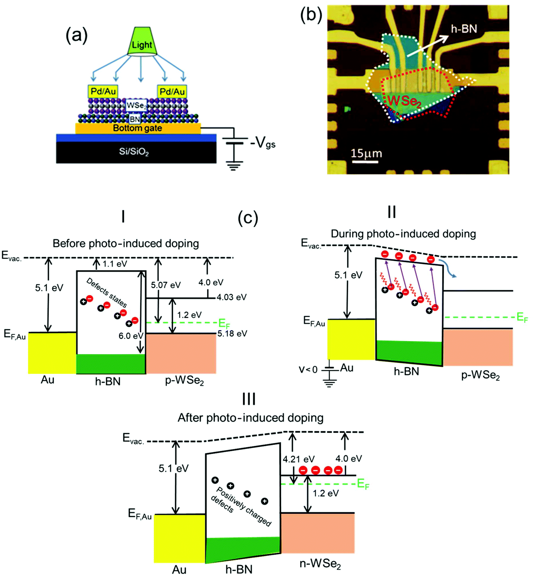 | ||
| Fig. 1 (a) Schematic illustration of a BN/WSe2 based FET under the illumination of light for obtaining a photo-induced effect. (b) Optical microscopy image of BN/WSe2 with Pd/Au electrodes. (c) I: Schematic of the band structure of the BN/WSe2 heterostructure before photo-induced doping; the work function value of p-WSe2 is estimated to be 5.07 eV calculated using KPFM measurements. II: Schematic of the photo-induced process, in which the incident photons of light first excite the electrons from donor-like states in BN. The photoexcited electrons can be injected into WSe2 under a negative gate stress voltage (−Vgs). III: The BN generates positively charged defects when Vgs and the light are off, and the work function value of n-WSe2 is estimated to be 4.21 eV using KPFM measurements. | ||
2D materials, such as WSe2, demonstrate semiconducting properties, and they may either show ambipolar behavior or p- or n-type conduction. The interface properties of 2D material-based FETs with metals are influenced by the conductive nature of the material. In this study, we discovered that Pd/WSe2 or Al/WSe2 interface properties could be either of the ohmic or the rectifying type depending on their work functions.
Initially, we fabricated BN/p-WSe2 heterostructures using exfoliated nanoflakes on a bottom gate electrode, as shown in Fig. 1b. The ohmic contribution can be observed in the log scale of the ID–VD characteristic corresponding to the p-WSe2 FET with Pd/Au electrodes (Fig. S2a†). Furthermore, to deduce the exact value of the work function of p-WSe2, we performed the KPFM measurements. The work function value is calculated using the following equation:
| ϕP-WSe2 = ϕtip + CPD, |
An exciting photodoping effect was established in WSe2 based FETs to invert p-type conduction into n-type, where the BN/p-WSe2 heterostructures were illuminated simultaneously with light of a wavelength of 220 nm for 7 min under a negative gate stress voltage (Vgs) of −10 V. From Fig. 2a, it is clear that the current on the electron side attains the same level, which demonstrates the electron doping effect. By increasing Vgs to −25 V, we observed that the current of the electron regime further increases, as shown in Fig. 2a. The photodoping treatment inverts WSe2 with p-type to an n-type semiconductor. Moreover, the ID–VD characteristic with non-ohmic contribution obtained as a result of Schottky contacts at the interface of n-type WSe2 with Pd/Au can be observed in the log scale of Fig. S2b.† Furthermore, the rectification ratio declines from 4.5 to 3.1, once the back-gate voltage (Vbg) is changed at the n-WSe2/(Pd/Au) junction from −15 to +15 V (Fig. S2b†). The work function calculated using the KPFM measurements after photodoping is estimated to be ∼4.21 eV, as shown in Fig. 1c. The photo-induced effect in WSe2 has consequently modified the work function. It is observed that the value of the work function for WSe2 declines (5.07 to 4.21 eV) as the p-type conduction is changed to n-type (Fig. 1c). The mechanism of photo-induced doping is initiated in the BN/p-WSe2 heterostructures because of the photosensitive excitation of the defect states or the point defects in BN nanoflakes. The incident photons of light can excite defect states (or donor-like states)26 in BN, as shown in Fig. 1c, which illustrates the photo-induced electron doping in BN/p-WSe2 heterostructures. Upon illumination, the electrons of the point defects inside BN are stimulated to the conduction band. The excited electrons entered into WSe2 under −Vgs. The localized ionized point defects in BN are positively charged, which can eliminate the influence of the electric field on BN throughout the process of photo-induced doping. The elimination of positively charged defects remains till the electric field in BN vanishes, and the ionized point defects remained in the interior of BN.26 The positive ionized point defect charges are observed inside BN, even if both the light and Vgs are switched off, which demonstrates a stable photo-induced doping effect in WSe2.
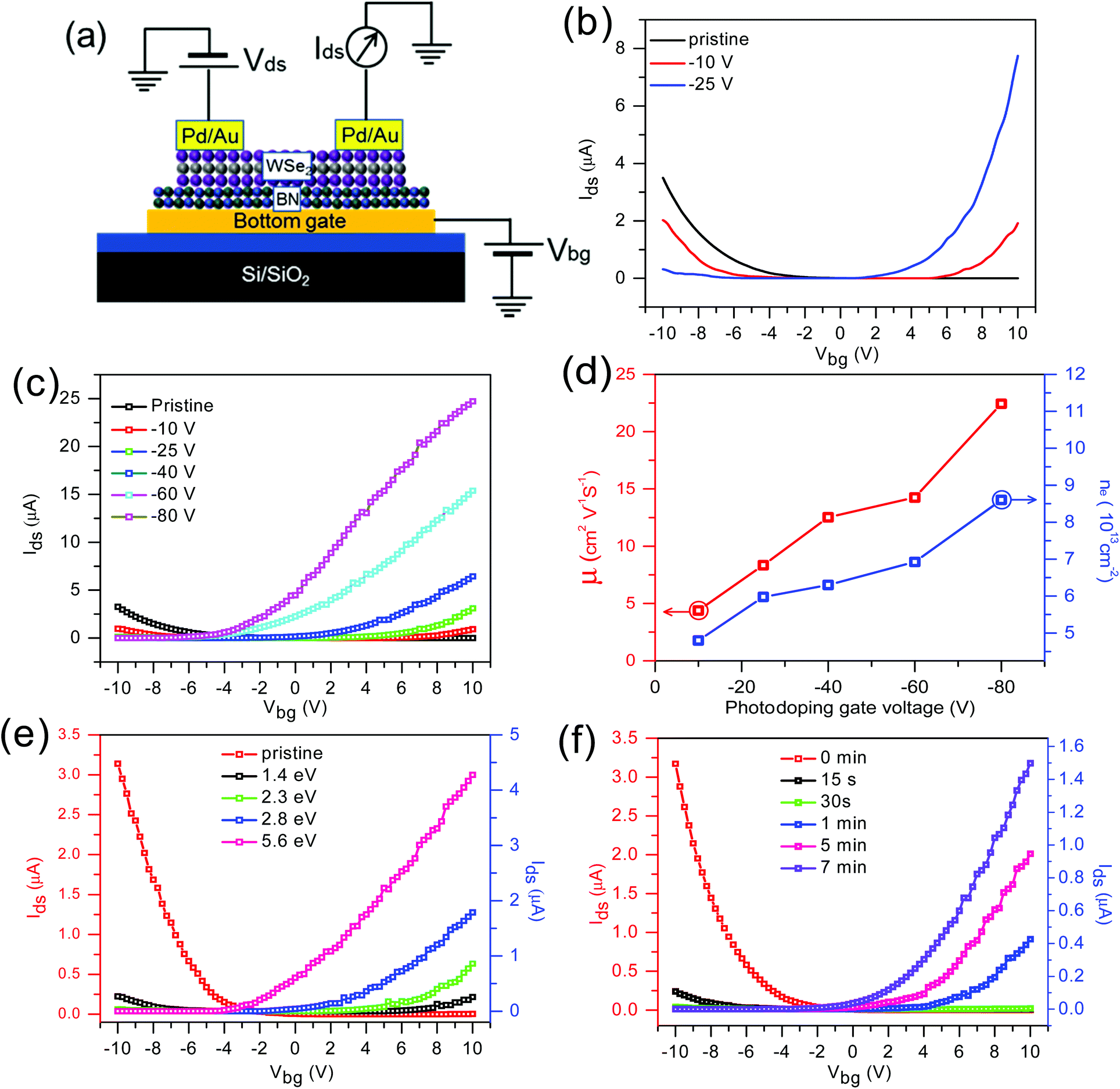 | ||
| Fig. 2 (a) Schematic illustration of a BN/WSe2 based FET after the photo-induced effect. (b) Transfer characteristics of pristine and doped BN/WSe2 FET devices at Vds = 0.5 V with a light of photon energy 5.6 eV for the illumination period t = 7 min at Vgs = −10 V and −25 V. The transfer curve indicates that p-WSe2 has transformed from hole domination to electron domination (n-WSe2). (c) Transfer characteristics of the BN/WSe2 FET device with respect to Vgs for t = 5 min at Vds = 0.5 V. The energy of incident photons is 2.3 eV. (d) Plot of electron concentration and mobility as a function of photo-induced gate voltage. (e) Transfer characteristics of the BN/WSe2 based FET device at Vds = 0.5 V with a different energy of incident photons for t = 5 min at Vgs = −10 V. (f) Transfer characteristics of the BN/WSe2 based FET device at Vds = 0.5 V for varied illumination times with an incident photon energy of 2.3 eV at Vgs = −10 V. | ||
Additionally, we validated the effect of the electron-photo-induced process on BN/WSe2 heterostructures by varying parameters, such as Vgs (Fig. 2c), photon energy (Fig. 2e), and light exposure duration (Fig. 2f). It is clear from the results that our devices have demonstrated an enhanced electron-photo-induced effect for all the aforementioned parameters. The dominant effect can be observed with modulation in the photo-induced gate voltage, as shown in Fig. 2c. The dominant electron doping effect establishes that the doping level of electrons in WSe2 nanoflakes could be modified by increasing Vgs. The carrier concentration of electrons (ne) can be calculated by using the following relationship:
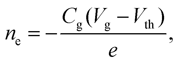
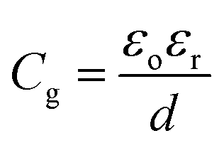 , where εo is the permittivity constant and d is the thickness of BN flakes. The value of the dielectric constant for a multi-layered BN flake is εr = 4,27 and Cg = ∼2.90 × 10⁻⁷ F cm−2 for BN with a thickness of 12.2 nm. Vth is the threshold voltage for electron transport, Vg is the back-gate voltage, and e is the electronic charge. For example, the electron concentration was derived as ∼8.6 × 1013 cm−2 at (Vgs = −80 V). The mobility (μFE) of n-WSe2 in a two-terminal FET configuration can be calculated using the following equation:
where W is the width and L is the length of the channel, the value of Cg for the BN substrate is ∼2.90 × 10⁻⁷ F cm−2, and
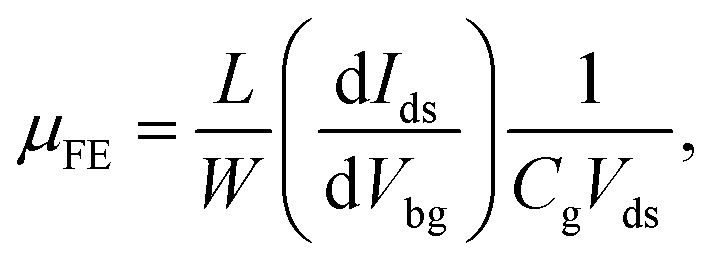
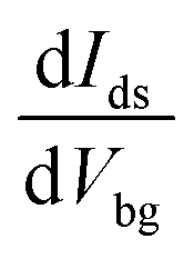 is the slope of the linear part of the transfer plot. For instance, the electron mobility was estimated to be ∼22 cm2 V−1 s−1 for Vgs = −80. The carrier concentration (ne) and electron mobility (μe) are shown in Fig. 2d.
Owing to the importance of photo-induced doping in WSe2, planar devices were assembled using a random doping strategy with a free photoresist, unlike previously reported homojunction diodes that required a photoresist to modify the doping level.28,29 Moreover, this method does not affect the properties of the metal electrodes in this device. The stability of n-type conduction in WSe2 is observed over 50 days, as shown in Fig. S5.†
This lateral WSe2 p–n diode was constructed on a thick BN flake having two bottom gate electrodes on the Si/SiO2 substrate (Fig. 4b). While performing photodoping by using deep UV light having an energy of 5.6 eV for 5 min at Vgs = −40, half of the area of the WSe2 flake was inverted to n-type, while half of the area remained p-type. The KPFM measurements were performed to determine the CPD value between the doped and undoped regions of WSe2 using the highly doped Si tips under ambient conditions. A CPD value of approximately 165 meV is observed between p-WSe2 and n-WSe2 on the BN substrate (Fig. 3). The value of potential difference in our case is greater than that of the lateral WSe2 homojunction diode (∼55 mV) obtained based on helium ion irradiation.30 It is comparable to that of the WSe2 homojunction (∼200 mV) obtained by H2 plasma treatment for an n-type doping process.31
 | ||
| Fig. 3 (a) KPFM image of the WSe2 flake at Vgs = −40 V. The line scans are denoted by the white line in the KPFM image. (b) The corresponding step profile height from the KPFM image as indicated. The value of contact potential difference between BN/p-WSe2 and BN/n-WSe2 is approximately 165 meV. | ||
Fig. 4a shows the schematic diagram of a planar p–n diode, while Fig. 4b shows an optical image. The metals Al/Au and Pd/Au were deposited on the n-WSe2 and p-WSe2 layers, respectively. The ID–VD characteristics of n-WSe2 and p-WSe2 demonstrate a linear behavior, thereby confirming the low resistivity of the metal contacts, as shown in Fig. S4.† Individual n-WSe2 and p-WSe2 flakes were inspected for their transfer characteristics, and the results obtained are shown in Fig. 4c. We examined the gate-dependent rectifying performance of the planar homojunction diode by utilizing the ionic liquid gating effect, as FETs based on ionic liquid gates have been widely studied owing to their small operational voltage.32–34Fig. 4d shows the typical rectifying behavior of the planar WSe2 homojunction diode under the influence of a low top gate voltage (VILg) changed from −2 to +2 V in a step of 0.5 V. The diode rectification behavior on a linear scale can be seen in Fig. S3.† It is observed from this figure that as VILg increases from −2 to −0.5 V, the current values decline proportionally in the forward and reverse bias regions; however, these values decline much more rapidly in the negative bias region than on the positive side, which produces a dominant change in the rectification ratio of up to ∼1.0 × 10⁵, as shown in Fig. 4e. When VILg increases further from −0.5 to +2 V, it can be observed that the reverse current is almost unaffected, while the current in the forward regime continues to decrease, causing a decline in the rectification ratio (Fig. 4d). The ionic liquid gate-dependent rectification behavior of the lateral WSe2 diode is due to the tunable built-in potential barrier at the homointerface of n-WSe2 and p-WSe2 under the influence of an external electric field. The transfer curve (Isd–VILg) is divided into four regimes by tuning VILg (Fig. S7a†). In the transfer curve, the four regimes are demarcated by a hump with two valleys. This implies that the diode functions exist in the regimes p–p+, p–n−, p−–n, and n–n+. In the p–p+ junction, the Fermi level of WSe2 is moved downward, nearer to the valence band (Fig. S7b†), under the influence of a high negative gate bias, and the holes become dominant in both the channels, that is in the doped n-WSe2 and undoped p-WSe2. Furthermore, the device exhibits p-type semiconducting characteristics (Fig. S7a†). With an increase in the gate voltage, the Fermi level moves up nearer to the bandgap (Fig. S7b†), and the electrons become intensely dominant in the doped channel of WSe2 owing to the creation of either one p–n− or p−–n junction. This improves the built-in potential at the homointerface and causes an enhancement in the diode performance. When the value of greater positive gate bias increases further, the Fermi level enters into the conduction band (Fig. S7b†); the electrons become dominant in both the channels, i.e. in the doped n-WSe2 and undoped p-WSe2, and the device then functions in the n–n+ junction and demonstrates an n-type semiconducting behavior (Fig. S7a†).
 | ||
| Fig. 4 (a) Schematic illustration of the lateral WSe2 p–n diode. (b) Optical image of the p–n diode. The right WSe2 channel on BN is electron-doped, while the one on the left remains pristine. (c) Transfer curves of p-WSe2 and n-WSe2 at Vds = 0.5 V as a function of Vbg. (d) Gate-dependent rectifying effect of the diode in the log scale. (e) Rectification ratio of the diode as a function of top gate ionic liquid gate voltage. (f) Ideality factor of the device at VILg = −0.5 V. | ||
In addition, we have examined the rectification ratio using different asymmetric electrodes of the pristine WSe2 flake without the photodoping. The diode rectification ratio is much higher (∼6.3 × 10⁴) at VILg = 0 V (Fig. 4e and f) than the rectification ratio (∼59) of the Pd/Au-(p-WSe2)-Al/Au device at Vbg = 0 without doping (Fig. S6†). When the p-WSe2 channel itself was examined, no rectification behavior was observed with Pd/Au contacts, as shown in Fig. S4a.† Similarly, no rectification effect was observed in the n-WSe2 channel with the Al/Au contacts, as shown in Fig. S4b.† In conclusion, the rectification in our diode is only due to the influence of the junction. Furthermore, to exclude the probability that the photodoping effect originated from the intrinsic deep level trap state in WSe2, we performed an experiment. We fabricated devices by stacking WSe2 nanoflakes on a thick BN flake with a part of its area placed on BN and the remaining area on SiO2. The heterostructure of BN and WSe2 was simultaneously illuminated under light and by applying −Vgs, and it was found that only a portion of the p-type WSe2 flake that is placed on BN was inverted to n-WSe2 during the photodoping treatment, while the area of the flake that is placed on SiO2 remained p-type. This experiment confirmed that the photodoping effect does not originate from the intrinsic deep level trap state in WSe2.
The ideality factor (n) of the diode was extracted by fitting to the equation35,36 as follows:
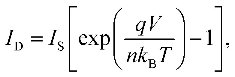
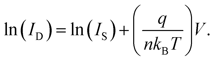
The value of n is extracted to be ∼1.0 at a gate bias of −0.5 V, as shown in Fig. 4f.
We further explored the optoelectronic response of the lateral WSe2 diode using a laser light with λ = 530 nm. Fig. 5a shows the photovoltaic characteristics of this lateral WSe2 diode. We calculated the photovoltaic parameters such as photoresponsivity  and
and  , where Iph = Iillumination − Idark, laser power Plaser = 10 mW cm−2, λ = 530 nm, and A is the junction area, c the speed of light, q the charge on electrons, and h is Planck's constant.37,38 We deduced that R of the WSe2 diode is 5.1 A W−1, which is much greater than that of the MoTe2-based homojunction diode.39 Furthermore, it is observed from Fig. 5b that under different powers of light illumination, the ID–VD curves of the device do not pass through the zero points of voltage and current, even when there is no applied voltage. The presence of a built-in potential in our device leads to Voc and Isc without an external electric field (Fig. 5b). The detected phenomenon is the distinct feature of lateral diodes, as compared to photodetectors40–42 or diodes based on mixed-dimensional heterostructures.
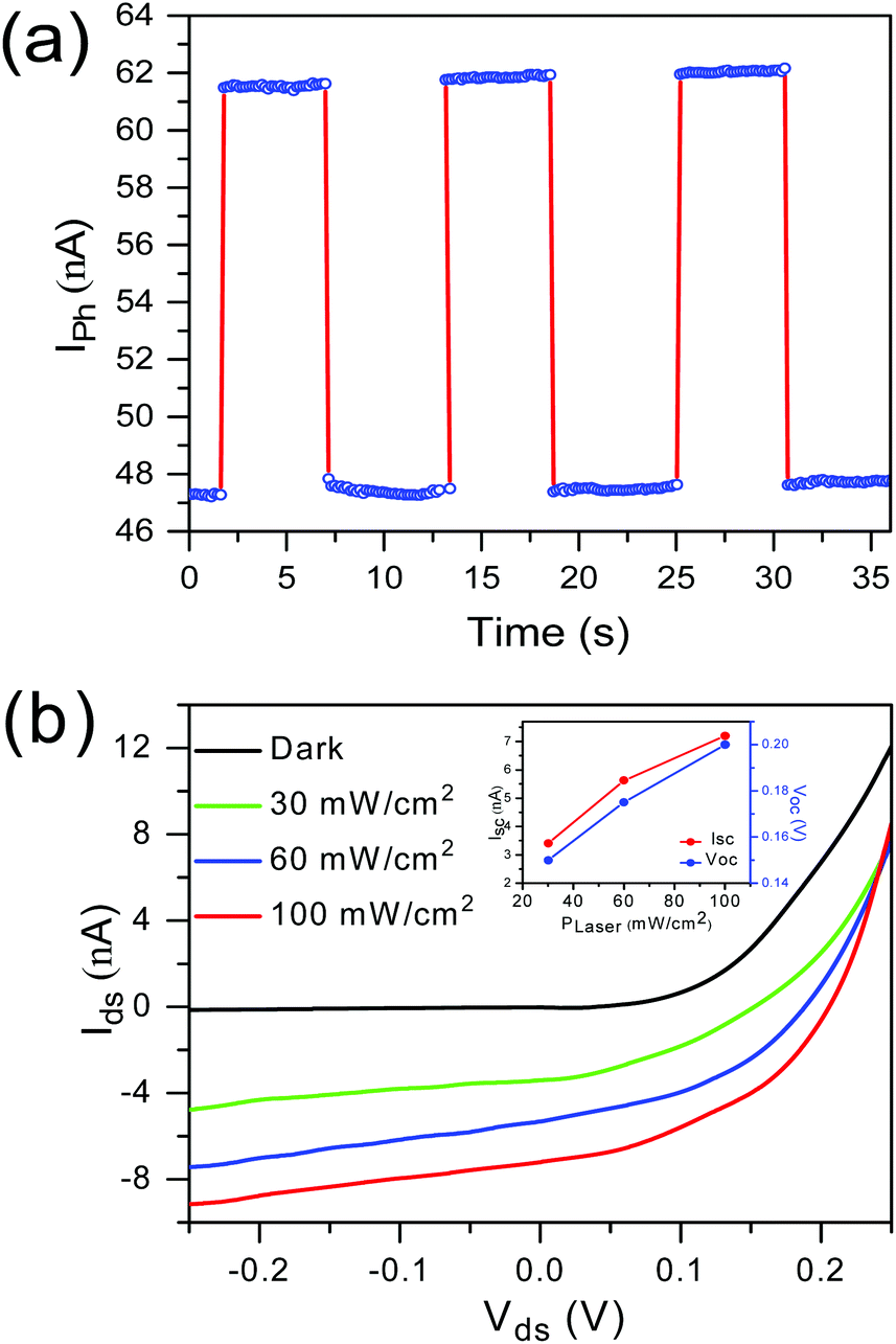 | ||
| Fig. 5 Photoresponse of a WSe2 homojunction p–n diode. (a) Photocurrent of the diode at Vds = 0.5 V under green laser light illumination between the ON and OFF states. (b) Output ID–VD characteristics of the diode under dark and light illumination. The inset shows Voc and Isc as a function of the laser power. | ||
Conclusion
In summary, we demonstrated a WSe2 homojunction diode by applying the photo-induced effect in BN/WSe2 heterostructures under the illumination of visible and deep UV light. It was revealed that with this photo-induced doping technique, FETs based on p-type WSe2 were inverted to n-WSe2, which can maintain a high electron mobility in h-BN/n-WSe2 heterostructures. To confirm this hypothesis, KPFM measurements were performed to deduce the work function values of p-WSe2 and n-WSe2 FETs as 5.07 eV and 4.21 eV, respectively. The KPFM measurements revealed the modification of the Fermi level in WSe2 owing to electron doping from donor-like states of h-BN under illumination because of the photo-induced gate voltage. They were also used to deduce the value of CPD between the doped and undoped junctions, which was estimated to be 165 meV. We used ohmic metal contacts for the planar homojunction diode by utilizing the ionic liquid gate and achieved a diode rectification ratio (∼105) with n = 1. In addition, excellent photovoltaic performances were demonstrated by these devices. Therefore, we consider that a stable and flexible charge doping technique within a single flake can be effective for electronic applications.Conflicts of interest
The authors declare no competing financial interests.Acknowledgements
This work was supported by the national research foundation of Korea (NRF) grant funded by the Korea government (MIST) (No. NRF 2019R1A2C2090443 and NRF-2017M3A7B4041987). This work is also funded by the Higher Education Commission (HEC) of Pakistan under the National Research Program for Universities (NRPU) with project no. HEC/R&D/NRPU/2017/7876.References
- S. Aftab and J. Eom, 2D Mater., 2019, 6, 035005 CrossRef.
- K. S. Novoselov, A. K. Geim, S. V. Morozov, D. Jiang, Y. Zhang, S. V. Dubonos, I. V. Grigorieva and A. A. Firsov, Science, 2004, 306, 666–669 CrossRef CAS PubMed.
- W.-M. Kang, S. Lee, I.-T. Cho, T. H. Park, H. Shin, C. S. Hwang, C. Lee, B.-G. Park and J.-H. Lee, Solid-State Electron., 2018, 140, 2–7 CrossRef CAS.
- J. Kang, W. Liu, D. Sarkar, D. Jena and K. Banerjee, Phys. Rev. X, 2014, 4, 031005 Search PubMed.
- H. Fang, S. Chuang, T. C. Chang, K. Takei, T. Takahashi and A. Javey, Nano Lett., 2012, 12, 3788–3792 CrossRef CAS PubMed.
- Y. Deng, Z. Luo, N. J. Conrad, H. Liu, Y. Gong, S. Najmaei, P. M. Ajayan, J. Lou, X. Xu and P. D. Ye, ACS Nano, 2014, 8, 8292–8299 CrossRef CAS PubMed.
- W. Hu and J. Yang, J. Mater. Chem. C, 2017, 5, 12289–12297 RSC.
- S. Aftab, M. F. Khan, P. Gautam, H. Noh and J. Eom, Nanoscale, 2019, 11, 9518–9525 RSC.
- N. Stander, B. Huard and D. Goldhaber-Gordon, Phys. Rev. Lett., 2009, 102, 026807 CrossRef CAS PubMed.
- J. S. Ross, P. Klement, A. M. Jones, N. J. Ghimire, J. Yan, D. Mandrus, T. Taniguchi, K. Watanabe, K. Kitamura and W. Yao, Nat. Nanotechnol., 2014, 9, 268 CrossRef CAS PubMed.
- A. Pospischil, M. M. Furchi and T. Mueller, Nat. Nanotechnol., 2014, 9, 257 CrossRef CAS PubMed.
- B. W. Baugher, H. O. Churchill, Y. Yang and P. Jarillo-Herrero, Nat. Nanotechnol., 2014, 9, 262 CrossRef CAS PubMed.
- C. Han, Z. Hu, L. C. Gomes, Y. Bao, A. Carvalho, S. J. Tan, B. Lei, D. Xiang, J. Wu and D. Qi, Nano Lett., 2017, 17, 4122–4129 CrossRef CAS PubMed.
- M. S. Choi, D. Qu, D. Lee, X. Liu, K. Watanabe, T. Taniguchi and W. J. Yoo, ACS Nano, 2014, 8, 9332–9340 CrossRef CAS PubMed.
- S. Roy, A. G. Joshi, S. Chatterjee and A. K. Ghosh, Nanoscale, 2018, 10, 10664–10682 RSC.
- A. C. Ferrari, F. Bonaccorso, V. Fal'Ko, K. S. Novoselov, S. Roche, P. Bøggild, S. Borini, F. H. Koppens, V. Palermo and N. Pugno, Nanoscale, 2015, 7, 4598–4810 RSC.
- H. Schmidt, F. Giustiniano and G. Eda, Chem. Soc. Rev., 2015, 44, 7715–7736 RSC.
- N. Ubrig, S. Jo, H. Berger, A. F. Morpurgo and A. B. Kuzmenko, Appl. Phys. Lett., 2014, 104, 171112 CrossRef.
- Y. Zhang, J. Ye, Y. Yomogida, T. Takenobu and Y. Iwasa, Nano Lett., 2013, 13, 3023–3028 CrossRef CAS PubMed.
- C. J. Benjamin, S. Zhang and Z. Chen, Nanoscale, 2018, 10, 5148–5153 RSC.
- J. Suh, T.-E. Park, D.-Y. Lin, D. Fu, J. Park, H. J. Jung, Y. Chen, C. Ko, C. Jang and Y. Sun, Nano Lett., 2014, 14, 6976–6982 CrossRef CAS PubMed.
- A. Nipane, D. Karmakar, N. Kaushik, S. Karande and S. Lodha, ACS Nano, 2016, 10, 2128–2137 CrossRef CAS PubMed.
- P. Zomer, S. Dash, N. Tombros and B. Van Wees, Appl. Phys. Lett., 2011, 99, 232104 CrossRef.
- L. Britnell, R. V. Gorbachev, R. Jalil, B. D. Belle, F. Schedin, M. I. Katsnelson, L. Eaves, S. V. Morozov, A. S. Mayorov and N. M. Peres, Nano Lett., 2012, 12, 1707–1710 CrossRef CAS PubMed.
- L. Britnell, R. Gorbachev, R. Jalil, B. Belle, F. Schedin, A. Mishchenko, T. Georgiou, M. Katsnelson, L. Eaves and S. Morozov, Science, 2012, 335, 947–950 CrossRef CAS PubMed.
- L. Ju, J. Velasco Jr., E. Huang, S. Kahn, C. Nosiglia, H.-Z. Tsai, W. Yang, T. Taniguchi, K. Watanabe and Y. Zhang, Nat. Nanotechnol., 2014, 9, 348 CrossRef CAS PubMed.
- J. Wang, F. Ma and M. Sun, RSC Adv., 2017, 7, 16801–16822 RSC.
- J. Y. Lim, A. Pezeshki, S. Oh, J. S. Kim, Y. T. Lee, S. Yu, D. K. Hwang, G. H. Lee, H. J. Choi and S. Im, Adv. Mater., 2017, 29, 1701798 CrossRef PubMed.
- W. Luo, M. Zhu, G. Peng, X. Zheng, F. Miao, S. Bai, X. A. Zhang and S. Qin, Adv. Funct. Mater., 2018, 28, 1704539 CrossRef.
- M. G. Stanford, P. R. Pudasaini, A. Belianinov, N. Cross, J. H. Noh, M. R. Koehler, D. G. Mandrus, G. Duscher, A. J. Rondinone and I. N. Ivanov, Sci. Rep., 2016, 6, 27276 CrossRef CAS PubMed.
- M. Tosun, L. Chan, M. Amani, T. Roy, G. H. Ahn, P. Taheri, C. Carraro, J. W. Ager, R. Maboudian and A. Javey, ACS Nano, 2016, 10, 6853–6860 CrossRef CAS PubMed.
- P. R. Pudasaini, J. H. Noh, A. Wong, A. V. Haglund, S. Dai, T. Z. Ward, D. Mandrus and P. D. Rack, ECS J. Solid State Sci. Technol., 2015, 4, Q105–Q109 CrossRef CAS.
- S. Zhang, N. Sun, X. He, X. Lu and X. Zhang, J. Phys. Chem. Ref. Data, 2006, 35, 1475–1517 CrossRef CAS.
- R. Misra, M. McCarthy and A. F. Hebard, Appl. Phys. Lett., 2007, 90, 052905 CrossRef.
- D. A. Neamen, Semiconductor physics and devices, McGraw-Hill, New York, 1997 Search PubMed.
- T. Banwell and A. Jayakumar, Electron. Lett., 2000, 36, 291–292 CrossRef.
- M. M. Furchi, A. Pospischil, F. Libisch, J. Burgdörfer and T. Mueller, Nano Lett., 2014, 14, 4785–4791 CrossRef CAS PubMed.
- L. Ye, H. Li, Z. Chen and J. Xu, ACS Photonics, 2016, 3, 692–699 CrossRef CAS.
- S. Aftab, M. F. Khan, P. Gautam, H. Noh and J. Eom, Nanoscale, 2019, 9518–9525 RSC.
- Z. Zheng, T. Zhang, J. Yao, Y. Zhang, J. Xu and G. Yang, Nanotechnology, 2016, 27, 225501 CrossRef PubMed.
- W. Zhang, M.-H. Chiu, C.-H. Chen, W. Chen, L.-J. Li and A. T. S. Wee, ACS Nano, 2014, 8, 8653–8661 CrossRef CAS PubMed.
- R. K. Chowdhury, R. Maiti, A. Ghorai, A. Midya and S. K. Ray, Nanoscale, 2016, 8, 13429–13436 RSC.
Footnote |
| † Electronic supplementary information (ESI) available. See DOI: 10.1039/d0nr00231c |
| This journal is © The Royal Society of Chemistry 2020 |