
 Open Access Article
 This Open Access Article is licensed under a
 Creative Commons Attribution 3.0 Unported Licence
All solution-processed ITO free flexible organic light-emitting diodes
Yolande
Murat
 *a,
Karlis
Petersons
b,
Deepak
Lanka
a,
Lars
Lindvold
b,
Leif
Yde
b,
Jan
Stensborg
b and
Martina
Gerken
a
*a,
Karlis
Petersons
b,
Deepak
Lanka
a,
Lars
Lindvold
b,
Leif
Yde
b,
Jan
Stensborg
b and
Martina
Gerken
a
aInstitute of Electrical Engineering and Information Technology, Kiel University, Kaiserstrasse 2, Kiel 24143, Germany. E-mail: ym@tf.uni-kiel.de; mge@tf.uni-kiel.de
bStensborg A/S, Riso Huse 50, 4000 Roskilde, Denmark
First published on 23rd September 2020
Abstract
Roll-to-roll (R2R) printing and coating techniques can be used for low cost and large-area mass production of organic electronic devices. While research in the photovoltaic field has developed R2R printed large-scale solar modules, research in solution-processed OLEDs has not progressed as far yet. In this work, we investigate all-solution processed OLEDs based on ink-jet printed silver bottom electrodes and spin-coating of all other layers. Ink-jet printing provides the advantages of mask-free patterning and non-contact manufacturing. As the top electrode, a conductive PEDOT:PSS formulation easily processable on organic layers due to a low contact angle is utilized. The all-solution processed top-emitting OLEDs achieve high luminance (7![[thin space (1/6-em)]](https://www.rsc.org/images/entities/char_2009.gif) 000 cd m−2) and an efficiency close to that of reference devices with evaporated electrodes: 4.2 cd A−1vs. 7.6 cd A−1, respectively. The shelf stability is also tested and after seven months, the all solution-processed encapsulated OLED retains 82% of its initial EQE.
000 cd m−2) and an efficiency close to that of reference devices with evaporated electrodes: 4.2 cd A−1vs. 7.6 cd A−1, respectively. The shelf stability is also tested and after seven months, the all solution-processed encapsulated OLED retains 82% of its initial EQE.
Introduction
Organic light emitting diodes (OLEDs) have been integrated in displays and lighting systems commercially available for a few years as they show several advantages such as high contrast, large viewing angle, lightweight, flexibility and a quick response compared to liquid crystal displays (LCDs). However, they are currently fabricated through an evaporation process which requires high vacuum, leading to a high cost and a low fabrication yield. On the other hand, roll-to-roll (R2R) printing and coating techniques under ambient conditions can be used for low cost and large-area mass production.1 The research in the organic electronics field has been focusing on this point, especially in organic photovoltaics (OPV) as the OPV stack usually has fewer layers than an OLED, facilitating the fabrication process. In 2018, Abbel et al. reviewed all the R2R printed organic electronic devices described in the literature and showed that a large number of studies focused on the OPV field.2 Researchers such as the Krebs or Galagan groups successfully managed to fabricate OPV modules by R2R printing.3–7 More recently, the R2R fabrication process has also been developed for perovskite solar cells.8 For emissive devices, Sandström et al. fabricated electrochemical cells (LECs) using the R2R slot die coating process.9 These devices consist of few layers since the mobile ions in the active layer lead to electrochemical doping when a voltage is applied. The process is simpler than for an OLED stack made of many layers even if the LEC emissive layer homogeneity can be an issue. In the Abbel review, only three papers on R2R printed OLEDs were described.10–12 More studies can be found based on sheet-to-sheet printing processes.13–19 But only a few studies reported all solution-processed OLEDs compared to OPVs.20–25The choice of the materials is the first step to address a low-cost R2R fabrication process. The widely used indium tin oxide (ITO) electrode represents almost half of the cost of an OLED device or an OPV device.26–29 Carter et al. revealed that the cost of a top-emitting OLED represents only 60% of the cost of a bottom-emitting OLED since the top-emitting OLED is ITO-free.26 ITO must be substituted by less costly materials. The ITO electrode is also too brittle, which is not compatible with the mechanical flexibility desired in the final product and during the fabrication process. Indeed, the R2R manufacturing requires flexible and durable substrates and materials. Concerning the substrates, polymer foils are widely used as they are highly flexible and exhibit good light transmission in the visible range. However, most of them have to be used at low temperature. Another disadvantage is the lack of dimensional stability. They also show poor UV stability and poor barrier properties to oxygen and water. Therefore, encapsulation is required. Metal foils are also utilized as flexible substrates. They can be used in a high temperature process and show good dimensional stability. They are an excellent barrier to oxygen and water. Their high surface roughness can be decreased by using polishing technique or by adding planarization layers. These foils are not transparent and top-emitting OLEDs or top-illuminated solar cells must be used. Besides the wide choice of substrates, top-emitting OLEDs have other advantages: they show a high aperture ratio in active-matrix displays which has attracted considerable attention these last few years. The light outcoupled from a bottom-emitting OLED is reduced by 25% due to the glass substrate having a different refractive index compared to organic layers, ∼1.5 and ∼1.8 respectively.30,31 Many studies of top-emitting OLEDs can be found in the literature but most of them use thermal evaporation to fabricate the OLED devices. Only a few studies use a solution process to fabricate the top-emitting OLEDs and in most of them, only one or two films are actually solution-processed.23,32–37
The main issue in the fabrication of solution-processed organic devices is the uniform deposition of materials on top of the active layer in an OPV device (or the emissive layer in an OLED device). Most of the active (or emissive) layers show hydrophobic properties while the materials deposited on top are in aqueous solutions. Poor adhesion of the top electrode on top of the active layer also leads to shorter stability, as the electrode will delaminate faster.38 Among transparent conductive solution processable materials, there are conductive polymer formulations such as PEDOT:PSS. Many PEDOT:PSS formulations are obtained from different suppliers. Agfa provides different inks called Orgacon. One of them, HIL-1005, is highly conductive (500 S cm−1) and has been used in several OPV and OLED devices.23,39Heraeus is the second main supplier of conductive PEDOT:PSS inks, with their brand named Clevios.40 In their paper, Lövenich et al. classified all the Clevios formulations according to their properties such as the viscosity, the pH and the conductivity range. The formulations having the highest conductivity are PH510, PH750 and PH1000, reaching 500, 750 and 1000 S cm−1, respectively. PEDOT PH1000 has been widely used as a bottom or top transparent electrode for OPV and OLED devices.21,41–47 However, the contact angle of PEDOT PH1000 and HIL-1005 on top of the active layer in OPV or the emissive layer in OLEDs is high, leading to a non-uniform layer. Zhou et al. measured a contact angle of 93° of PH1000 on top of P3HT:PCBM.46
To improve the layer uniformity, three methods have been reported in the literature. An interlayer can be introduced between the active layer and PH1000 layer, such as the low conductive PEDOT CPP in the Zhou work: the contact angle of this ink on top of P3HT:PCBM is 31°.46 We can reasonably think that successive deposition of two PEDOT:PSS layers can lead to dissolution problems, even if it is not mentioned in this paper. Another method is to include additives in the PEDOT:PSS formulation to decrease its contact angle and increase its adhesion property.20,48 However, the conductivity should be carefully controlled as the additives usually decrease it. The last method involves a transfer: the top electrode is first deposited on a substrate such as glass or quartz and then transferred to the organic device through a PDMS stamp. In 2019 Park et al. used this technique with ink-jet printing to design properly the top electrode.23 A PDMS stamp was further pressed in order to peel off the PEDOT:PSS layer. The adhesion and thus the transfer can be improved by adding additives in the PEDOT:PSS ink such as D-sorbitol. However, Park et al. observed an increase of the sheet resistance and chose carefully the D-sorbitol concentration. The sheet resistance of the optimized PEDOT:PSS film reaches 260.6 Ω □−1. Even if this method is efficient and leads to performant OLEDs, it involves many steps which can increase the fabrication time and cost. In their paper reporting all the PEDOT:PSS formulation from Heraeus, Lövenich et al. mentioned the highly conductive F HC Solar, reaching 600 S cm−1. The contact angle of this material is only 10° on top of UV-ozone cleaned ITO and lower than 30° on top of P3HT:PCBM. No additives or interlayers are needed to form a uniform layer. This material is surprisingly used only in a few studies in the literature and never used in an OLED device to our knowledge.49–51
The issue of the poor wetting of an electrode material on top of the emissive area also arises when a hole-injection layer (HIL) material is deposited on top of the emissive area. PEDOT:PSS Al4083 is widely used as a HIL layer in direct devices but it is rather difficult to form a homogeneous layer in an inverted device. In 2018 Park et al. reported the successful deposition of PEDOT:PSS Al4083 in an inverted OLED device by diluting the solution with ethanol.48 Alcohol-based dispersions using metal oxides such as MoOx or WOx have been successively used in inverted OPV and OLED devices. They guarantee proper wetting on top of organic materials. The WOx nanoparticles have a smaller size increasing the surface energy and stabilizing the solution without the use of binders. When a binder is used, a post-treatment such as plasma is required to establish the electronic functionality of the metal oxide film. Stubhan et al. showed that using WOx nanoparticles requires only annealing at 80 °C as post-treatment, making them good candidates for a solution processable HIL.52
To fabricate all solution-processed organic devices, either a transparent or semi-transparent stack can be chosen by using two transparent electrodes based for example on PEDOT:PSS.20 Another direction is to integrate an opaque and reflective electrode into the structure. Usually, ink-jet printed Ag is used.23,53 The main advantage of ink-jet printing is the possibility to print patterned films in one printing without the use of any mask. However, this technique is limited to the low-viscous inks (1–40 mPa s). Slot-die coating is widely used as the viscosity requirement range is much larger: 1–10000 mPa s. With this technique, stripes can be coated. To reach a better resolution of the coated layers, the research has been focused on laser patterning: a large stripe is coated and then separated in different narrower stripes by using laser ablation. It minimizes the dead area between each cell in OPV modules. It is also used to pattern OLEDs. However, the laser patterning becomes challenging for a printed Ag film due to its high roughness, yet high-resolution ink-jet printing can be efficiently used, as shown by Galagan et al. in an OPV module.3
In this work, we report all solution-processed top-emitting inverted OLEDs with an ink-jet printed Ag bottom electrode and spin-coated transparent top electrode. This one is based on a PEDOT:PSS formulation tested for the first time in an OLED device, Clevios F HC Solar (Heraeus). Its two main advantages are its high conductivity (600 S cm−1) and a low contact angle, improving the deposition on top of the emissive layer. Devices with and without a HIL based on WOx are tested and compared. The OLED size is defined by the ink-jet printed Ag bottom electrode. The top electrode is spin-coated as a stripe, which can be easily done by the slot die coating or blade coating process, without the use of any mask.
Results and discussion
Fig. 1 shows the OLED stacks fabricated in this work and the energetic diagram. They are all based on the fluorescent polymer Super Yellow. It should be noted that each device is optimized to reach the best performance. The electron injection layer (EIL) and electron transport layer (ETL) were optimized in a previous work. They are made of zinc oxide (ZnO) nanoparticles and polyethylenimine ethoxylated (PEIE).54 This polymer reduces the work function of the cathode, favoring the electron injection in the Super Yellow LUMO level. We show in a previous work that the use of a hole blocking layer is required.55 A small molecule 1,3,5-tris(N-phenylbenzimidazol-2-yl) (TPBi) is used and directly mixed in the PEIE ink.55 This process avoids the deposition of an ultra-thin PEIE layer, which is difficult to up-scale in the R2R process. For the reference device shown in Fig. 1(a), the HIL/top electrode is evaporated. A trilayer is used: MoOx/Ag/MoOx. It is well-known in the literature that using a capping layer on top of a thin layer of Ag increases the transmittance of the trilayer, allowing a higher light extraction.56 It also allows adjusting the microcavity in order to increase the OLED efficiency. In our reference structure, the highest efficiency is obtained for a 50 nm thick capping layer while the Ag layer thickness is kept as 15 nm.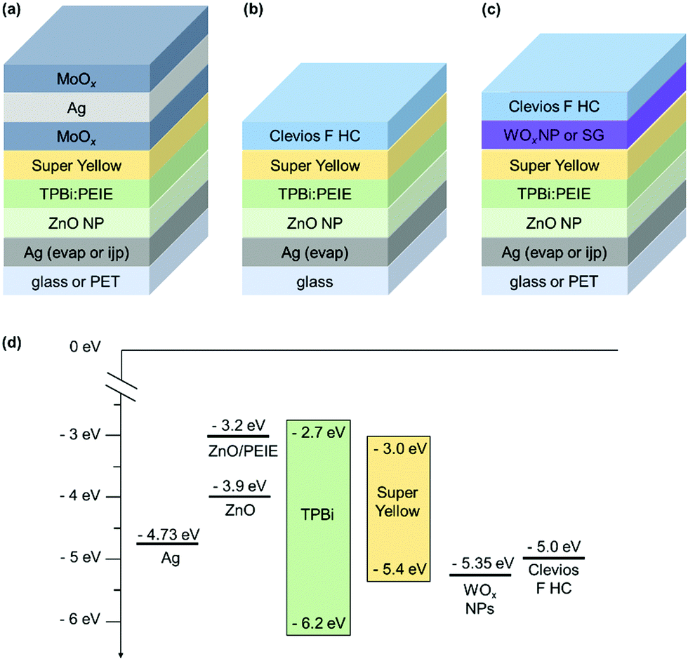 | ||
| Fig. 1 Top-emitting inverted OLED architectures based on Super Yellow. (a) Reference device with an evaporated HIL/top electrode. (b) Device without any HIL and spin-coated top electrode based on a highly conductive PEDOT:PSS, Clevios F HC. (c) Device with a spin-coated HIL/top electrode, the HIL is WOx (nanoparticles or from a sol–gel method). The bottom electrode is either evaporated Ag on glass, or ink-jet printed Ag on PET (for (a and c)). (d) Energetic diagram of the structure (c) with WOx nanoparticles.52 | ||
Fig. 1(b) and (c) show the OLED devices with a solution-processed HIL/top electrode. Three different architectures are studied: one without any HIL (b), one with WOx nanoparticles and the last one with the WOx sol–gel (c). They are all based on the same spin-coated top electrode made of a highly conductive PEDOT:PSS, Clevios F HC. The sheet resistance of a 180 nm thick Clevios F HC thin film is measured by the 4 probe method and reaches 90 ± 12 Ω □−1. The WOx sol–gel method is adapted from the work of Zang et al., where a tungsten(VI) ethoxide precursor solution (W(OEt)6) is diluted in isopropanol 1:80 (v/v) and spin-coated at 4000 rpm.20 In our work, different ratios have been tested while keeping 4000 rpm as the speed parameter and 1:100 led to the highest efficiency. The precursors can harm the organic layers.57 While depositing a thickest WOx layer (75 nm), the photoluminescence of SY decreases. However, in our OLED device, the layer is thin and the photoluminescence of SY remains constant, even after a longer storage time. For the WOx nanoparticle (NP) deposition, we use the commercial ink without any dilution as it was done previously in the literature for direct and inverted OPV devices.52,58,59 Stubhan et al. successfully fabricated OPV devices by using the same commercial ink.52 They deposited by doctor-blade the ink on ITO for the direct device and on the active layer for the inverted device. They obtained the highest performances for a 32 nm thick layer annealed for 5 min at 80 °C. They also measured the energy level of WOx NPs by using a Kelvin Probe in air and found it to be −5.35 eV. Meyer et al. reported previously that the work function of WOx is −6.4 eV but decreases after air exposure. In our case, after WOx NP deposition and annealing, we spin-coated the top electrode in air as PEDOT:PSS contains water, exposing the WOx layer to air. We can consider that the WF of WOx is closer to −5.35 eV than −6.4 eV. According to their supplier, the HOMO level of SY is −5.4 eV and the energy level of Clevios F HC is −5.0 eV. Adding the WOx NPs as in the interlayer reduces slightly the energetic barrier and allows a better hole injection in the SY layer, as shown in Fig. 1(d). We measure the Clevios F HC contact angle four times on different sample spots. The average and standard deviation is 10.5 ± 0.9°, 11.0 ± 0.7° and 8.7 ± 0.8° on glass, PET and ITO-covered glass substrates, respectively. The last value is similar to Heraeus measurement (10°) and can be validated. We measure the PEDOT F HC contact angle on different spin-coated thin films. It is found to be 22.7 ± 1.6° on top of glass/Super Yellow. This low contact angle guarantees proper wetting of Clevios F HC on top of the SY thin film during spin-coating. It slightly decreases when the SY thin film is covered by WOx. 17.9 ± 0.8° and 21.0 ± 0.8° are obtained for glass/SY/WOx sol–gel and glass/SY/WOx NPs, respectively. Using these two interlayers is attractive for a better charge injection, as discussed before, but also for the process itself. In our study, the bottom electrode is first deposited by thermal evaporation. Once the solution process to deposit the HIL/top electrode is optimized, we use ink-jet printed Ag as the bottom electrode.
Evaporated bottom electrode
Fig. 2(a) and (b) show the device characteristics of the optimized OLEDs built on top of glass substrates covered by the evaporated Ag cathode. The HIL/top anode is deposited by spin-coating except for the reference device, for which the MoOx/Ag/MoOx layers are evaporated. Its turn-on voltage (Von), which is defined at 1 cd m−2, is around 2.3 V. This is a standard value for an OLED based on Super Yellow. As expected, the OLED device with a single layer of Clevios F HC (i.e. without HIL) has a much higher turn-on voltage (5.1 V) than the reference device. When an HIL interlayer is added between SY and Clevios F HC, the turn-on voltage is reduced reaching 2.3 and 2.8 V for the devices with a WOx layer made from nanoparticles and sol–gel, respectively. Clevios F HC does not inject efficiently the holes at the low voltages despite the rather low energetic barrier with the HOMO level of Super Yellow. However, at higher voltages, the JV characteristics of the device processed top electrode reach high luminances, around 15000 cd m−2 at 14 V. For the same voltage, with V > 4 V, the device including sol–gel WOx shows a lower current density but a similar luminance value than the device using WOx nanoparticles. It leads to higher current and power efficiencies as shown in Fig. 2(b). The reference device exhibits no roll-off of the efficiency with the increase of the luminance, meaning that the charges are well-balanced even at high current density (300 mA cm−2). An efficiency roll-off is observed for the devices with a spin-coated top electrode. In particular, the power efficiency decreases for the devices with WOx: the efficiency is divided by 2 at 15000 cd m−2. It is probably due to a charge imbalance as described by Murawski et al. for fluorescent emitters.60 The hole injection is not effective enough at high voltages. Besides, the power efficiency shows a larger roll-off than the EQE as it takes into account the voltage applied and so the resistive losses. They are due to the energy barrier, low charge-carrier mobilities and the electrode sheet resistance. Clevios F HC has a higher sheet resistance than the evaporated top electrode, explaining also this higher roll-off. Nevertheless, at low luminance (under 2000 cd m−2), the devices with a spin-coated HIL/top electrode are more performant than the reference device, making them attractive.
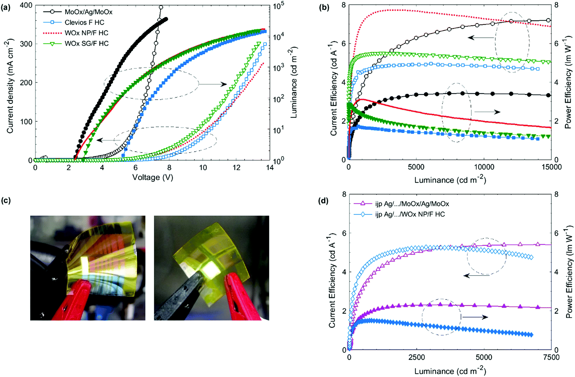 | ||
| Fig. 2 Inverted top-emitting OLEDs built on glass/evaporated Ag ((a and b)) and on PET/ink-jet printed Ag ((c and d)). The HIL/top electrode is varied for the different devices. (a and b) The first OLED device has an evaporated MoOx/Ag(15 nm)/MoOx (black circle) and the other devices have a solution-processed HIL/top electrode: Clevios F HC (blue square), WOx nanoparticle/Clevios F HC (red dashed line) and WOx sol–gel/Clevios F HC (green inverted triangle). (c) Photograph of the flexible OLED devices based on an ink-jet printed Ag bottom cathode and either an evaporated MoOx/Ag(15 nm)/MoOx (left) or spin-coated WOx/F HC (right). (d) Efficiencies of the flexible OLEDs based on an ink-jet printed Ag bottom cathode with evaporated MoOx/Ag(15 nm)/MoOx (pink triangle) or solution-processed WOx NP/F HC (blue diamond). | ||
For every parameter, 2 samples each containing 8 OLEDs are fabricated, leading to a number of 16 OLEDs for each parameter. Table 1 summarizes the averaged maximal efficiencies and EQE measured for different OLED structures. The reference device, with evaporated bottom and top electrodes, reaches a maximal EQE of 2.6 ± 0.2%. When the evaporated HIL/top electrode is replaced by a single spin-coated Clevios F HC layer, the EQE decreases to 1.8 ± 0.2%, which is still relatively high for a device without the HIL. The EQE increases when a WOx layer is added and the OLED device with WOx nanoparticles is the most efficient: 2.4 ± 0.4% is obtained which is close to that of the evaporated reference device. We can observe a higher standard deviation, which is probably due to the nanoparticles themselves. It is difficult to control their size and they can also form aggregates. An ultrasonic treatment of the commercial ink was done before the deposition. It breaks the largest aggregates and increases the coating homogeneity.
| Bottom cathode | Top anode | Structure | Max. current efficiency (cd A−1) | Max. power efficiency (lm W−1) | Max. EQE (%) | Turn-on voltage (V) |
|---|---|---|---|---|---|---|
| Glass/Ag (evaporated) | Evaporated | MoOx/Ag/MoOx | 7.6 ± 0.5 | 3.7 ± 0.4 | 2.6 ± 0.2 | 2.3 |
| Solution-processed | Clevios F HC | 4.0 ± 0.4 | 1.4 ± 0.5 | 1.8 ± 0.2 | 5.1 | |
| WOx NP/F HC | 6.3 ± 0.9 | 2.1 ± 0.6 | 2.4 ± 0.4 | 2.3 | ||
| WOx SG/F HC | 5.0 ± 0.4 | 2.5 ± 0.2 | 2.1 ± 0.1 | 2.8 | ||
| WOx NP/F HC | 4.2 ± 0.7 | 0.95 ± 0.3 | 1.7 ± 0.3 | 5.0 | ||
| PET/Ag (ink-jet printed) | Evaporated | MoOx/Ag/MoOx | 4.9 ± 0.8 | 1.6 ± 0.7 | 1.9 ± 0.3 | 2.7 |
Ink-jet printed bottom electrode
In the previous part, the bottom electrode is a silver layer deposited by thermal evaporation. In order to fabricate all solution-processed OLEDs, the evaporated Ag layer is replaced by an ink-jet printed Ag film. For the top electrode, we compare again an evaporated stack (MoOx/Ag/MoOx) and a spin-coated HIL/anode: WOx NP/Clevios F HC as this layer led to the highest efficiencies and the lowest turn-on voltages. The metal complex Ag ink is deposited on PET substrates via a drop-on-demand ink-jet printing technique. The dots per inch (DPI) are varied: 200, 400 and 800 DPI. The conductivity is the first important parameter for a material used as an electrode. The sheet resistance is measured by using the four probe method. 200 DPI, 400 DPI and 800 DPI samples lead to 17.4 ± 2.2, 2.3 ± 0.5 and 1.2 ± 0.6 Ω □−1. Increasing the DPI during the ink-jet process decreases the sheet resistance due to the higher density and the better homogeneity of the layer. The 800 DPI Ag coated substrate is chosen for the fabrication of top-emitting OLEDs. The RMS roughness of the 800 DPI Ag coated substrate is measured by laser interference and is 6 ± 1 nm. It is slightly larger than that of PET/ITO found in the literature (3.32 ± 0.53 nm)61 and similar to those of other printed Ag layers.24 The roughness and the sheet resistance are low enough to build efficient OLEDs on top of the ink-jet printed Ag.The same OLED fabrication process is used as in the previous part. For the OLED device with an evaporated top electrode, a 12 mm wide Ag stripe is printed leading to an emissive area of 10 mm2. For the all-solution processed device, four rectangular Ag areas are ink-jet printed and the top PEDOT:PSS electrode is spin-coated as a stripe, as shown in Fig. 2(c). The emissive area is around 16 mm2. For every parameter, 3 samples are fabricated, each having 4 OLEDs. It leads to a number of 12 OLEDs for every parameter.
Table 1 shows the maximal efficiencies and EQE of these devices. Both devices achieved 70% of the EQE of the reference device (evaporated bottom electrode). The turn-on voltage slightly increases from 2.3 V to 2.7 V for the OLED with an evaporated top electrode, as shown in Table 1. For the all solution-processed OLED, the Von increase is more important, reaching 5.0 V.
Stability measurements
After their fabrication and characterization, the encapsulated OLED devices are stored under ambient conditions. The JVL characteristics are measured again seven months later. Fig. 3 shows the JVL characteristics for two OLED devices. Device A corresponds to the stack with both evaporated Ag electrodes on glass, and device B is an all solution-processed OLED based on ink-jet printed Ag on PET as a bottom electrode and spin-coated WOx NP/Clevios F HC. It has to be noted that a PET foil is a moisture and oxygen reservoir. Pet foils are usually degassed before the OLED fabrication. In our work, this step is simplified by heating the ink-jet printed Ag samples in a glovebox at 70 °C since heating under vacuum could not be done. Device B, built on PET, might be in the presence of a higher oxygen content than device A built on glass.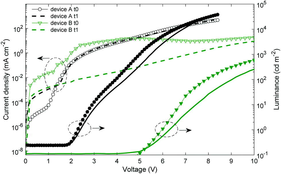 | ||
| Fig. 3 JVL characteristics of encapsulated top-emitting OLEDs after fabrication (t0) and after seven months (t1). The samples were stored under ambient conditions. Device A has the following stack: glass/Ag/ZnO/TPBi:PEIE/SY/MoOx/Ag/MoOx with evaporated Ag electrodes. Device B corresponds to the all solution-processed OLED, for which the electrodes are replaced by an ink-jet printed Ag layer on PET and a spin-coated WOx/Clevios F HC layer. | ||
The device with both evaporated electrodes (device A) has a higher leakage current after 7 months. It can be due to Ag diffusion into the emissive layer.62 At higher voltages, the current density is similar and the luminance is slightly lower. The averaged maximal EQE is 2.7 ± 0.1% after 7 months (vs. 2.6 ± 0.2% after the fabrication). The shelf stability of this device structure is rather good once the device is encapsulated. The all solution-processed OLED (device B) has an averaged maximal EQE equal to 1.4 ± 0.1% after 7 months, namely a decrease of 18% compared to its initial value indicated in Table 1.
Experimental
The fabrication process is conducted in a cleanroom environment. The flexible OLEDs are fabricated by using a heat stabilized 125 μm thick PET foil (Melinex ST505) supplied by Dupont Teijin Films. 25 × 25 mm2 PET and glass substrates are cleaned by ultrasonication in acetone and isopropanol for 10 minutes and heated for 15 minutes at 100 and 160 °C, respectively. The first layer, the silver electrode, is deposited either by thermal evaporation or by ink-jet printing. The process for the evaporated Ag is the following: an oxygen plasma treatment (5 min, 300 W) is first applied to the glass substrates in order to remove organic residues at the surface and to improve the adhesion of the evaporated silver layer. A thin layer of tungsten oxide (1–2 nm) is evaporated on top of the substrate to also increase Ag adhesion on glass, followed by the evaporation of a 100 nm thick Ag layer. The substrates are transferred directly to a glovebox under a nitrogen environment. The ink-jet printed Ag layer is fabricated in the Stensborg A/S laboratory. The Ag layer is made by using a proprietary low viscosity Ag metal complex ink from Stensborg A/S. A setup with Dimatix Polaris PQ-512 printheads is used to deposit the metal ink onto the substrate. After the metal ink is deposited, the sample is placed in a 160 °C oven to cure the ink, forming the solid Ag layer in the previously deposited pattern.The inverted OLED is fabricated in the following device configuration: substrate/Ag/ZnO/TPBi:PEIE/SuperYellow/HTL/PEDOT:PSS with different tested HTL materials based on WOx. For every material, the spin-coating is processed in a static method. The solution is first deposited on top of the substrate and the sample is afterwards rotated. Zinc oxide nanoparticles (Genes’ ink), previously mixed for 5 min in an ultrasonic bath to break the large aggregates, and a blend of TPBi:PEIE (Lumtec and Sigma-Aldrich) are successively spin-coated under a N2 atmosphere on top of the Ag substrate: 2500 rpm for 60 s and 1000 rpm for 60 s, respectively. The TPBi:PEIE blend preparation is described in our previous work.54 Both layers are annealed for 10 min at 100 °C. A solution of 5 mg mL−1 of Super Yellow (PDY-132, Merck) in toluene is spin-coated at 1000 rpm, leading to an 85 nm thick layer. The WOx sol–gel recipe is adapted from the work of Zang et al.63 A tungsten(VI) ethoxide precursor solution (W(OEt)6) (5% w/v in ethanol, abcr GmbH) is diluted in isopropanol 1:100 (v/v), spin-coated at 4000 rpm and converted in an inert atmosphere. We use WOx nanoparticles (Nanograde provided by Sigma-Aldrich) and follow the recipe of Stubhan et al.52 Prior to the deposition, the commercial ink is mixed in the ultrasonic bath for 10 min to break the large aggregates, spin-coated at 4000 rpm for 60 s and then annealed for 10 min at 100 °C. Wafer tape stripes are applied to design the top electrode. The top electrode is made of the highly conductive polymer Clevios F HC provided by Heraeus. This ink is spin-coated in an ambient atmosphere as its formulation contains water. 2000 rpm for 60 s leads to a 180 nm thick layer. The annealing at 100 °C for 10 min is performed in the glovebox again, as the encapsulation. Before the encapsulation, we add contacts with silver paste to the all solution-processed OLED. It does not influence the OLED performance and allows the characterization in our measurement set-up. We use a glass substrate and the Delo Katiobond glue to encapsulate the non-flexible OLEDs. The glue is cured 15 min under UV light in the glovebox. For the flexible OLEDs, we encapsulate both OLED sides with a flexible 3M foil and the Delo Photobond glue. The UV-curing also lasts for 15 min. For the stability study, the flexible OLEDs are encapsulated with a glass substrate and the Delo Katiobond glue in order to compare only the stack itself with the reference device and not the encapsulation.
The current density–voltage–luminance (JVL) characteristics are recorded using two Source Measure Units (SMUs), Keithley 2400, and a silicon photodiode. The contact angle is measured through a fully automatic measuring device provided by Dataphysics (OCA50).
Conclusions
In this paper, we successfully demonstrated all-solution processed flexible top-emitting OLEDs based on an inkjet-printed silver bottom electrode and the Clevios F HC formulation as a top electrode. This PEDOT:PSS formulation shows interesting properties such as a low contact angle on organic layers, a high transmittance and a low sheet resistance. Combining Clevios F HC with WOx nanoparticles as the HIL and an evaporated bottom electrode led to top-emitting OLEDs reaching 6.3 cd A−1vs. 7.6 cd A−1 for the reference device with an evaporated HIL/top electrode. The all solution-processed flexible OLEDs had a maximum current efficiency of 4.2 cd A−1. The device structure presented here is suitable for a roll-to-roll (R2R) fabrication process and forms the basis for the next steps. In this paper, we also demonstrated that using only PEDOT F HC as the HIL and the top electrode leads to acceptable efficiencies, which simplifies greatly the process and reduces the fabrication cost. Moving towards R2R printing and coating fabrication techniques must also go through the simplification of the OLED structure.Conflicts of interest
The authors declare no conflict of interest.Acknowledgements
The authors acknowledge support from Interreg (Project Rollflex, 1_11.12.2014).Notes and references
- F. Machui, M. Hösel, N. Li, G. D. Spyropoulos, T. Ameri, R. R. Søndergaard, M. Jørgensen, A. Scheel, D. Gaiser, K. Kreul, D. Lenssen, M. Legros, N. Lemaitre, M. Vilkman, M. Välimäki, S. Nordman, C. J. Brabec and F. C. Krebs, Energy Environ. Sci., 2014, 7, 2792–2802 RSC.
- R. Abbel, Y. Galagan and P. Groen, Adv. Eng. Mater., 2018, 20, 1–30 CrossRef.
- Y. Galagan, H. Fledderus, H. Gorter, H. H. tMannetje, S. Shanmugam, R. Mandamparambil, J. Bosman, J. E. J. M. Rubingh, J. P. Teunissen, A. Salem, I. G. deVries, R. Andriessen and W. A. Groen, Energy Technol., 2015, 3, 834–842 CrossRef CAS.
- T. R. Andersen, H. F. Dam, M. Hösel, M. Helgesen, J. E. Carlé, T. T. Larsen-Olsen, S. A. Gevorgyan, J. W. Andreasen, J. Adams, N. Li, F. Machui, G. D. Spyropoulos, T. Ameri, N. Lemaître, M. Legros, A. Scheel, D. Gaiser, K. Kreul, S. Berny, O. R. Lozman, S. Nordman, M. Välimäki, M. Vilkman, R. R. Søndergaard, M. Jørgensen, C. J. Brabec and F. C. Krebs, Energy Environ. Sci., 2014, 7, 2925–2933 RSC.
- C. M. Amb, M. R. Craig, U. Koldemir, J. Subbiah, K. R. Choudhury, S. A. Gevorgyan, M. Jørgensen, F. C. Krebs, F. So and J. R. Reynolds, ACS Appl. Mater. Interfaces, 2012, 4, 1847–1853 CrossRef CAS.
- S. A. Gevorgyan, A. J. Medford, E. Bundgaard, S. B. Sapkota, H. F. Schleiermacher, B. Zimmermann, U. Würfel, A. Chafiq, M. Lira-Cantu, T. Swonke, M. Wagner, C. J. Brabec, O. Haillant, E. Voroshazi, T. Aernouts, R. Steim, J. A. Hauch, A. Elschner, M. Pannone, M. Xiao, A. Langzettel, D. Laird, M. T. Lloyd, T. Rath, E. Maier, G. Trimmel, M. Hermenau, T. Menke, K. Leo, R. Rösch, M. Seeland, H. Hoppe, T. J. Nagle, K. B. Burke, C. J. Fell, D. Vak, T. B. Singh, S. E. Watkins, Y. Galagan, A. Manor, E. A. Katz, T. Kim, K. Kim, P. M. Sommeling, W. J. H. Verhees, S. C. Veenstra, M. Riede, M. Greyson Christoforo, T. Currier, V. Shrotriya, G. Schwartz and F. C. Krebs, Sol. Energy Mater. Sol. Cells, 2011, 95, 1398–1416 CrossRef CAS.
- S. Strohm, F. Machui, S. Langner, P. Kubis, N. Gasparini, M. Salvador, I. McCulloch, H. J. Egelhaaf and C. J. Brabec, Energy Environ. Sci., 2018, 11, 2225–2234 RSC.
- Y. Galagan, F. Di Giacomo, H. Gorter, G. Kirchner, I. de Vries, R. Andriessen and P. Groen, Adv. Energy Mater., 2018, 8, 1–7 Search PubMed.
- A. Sandstrom, H. F. Dam, F. C. Krebs and L. Edman, Nat. Commun., 2012, 3, 1–5 Search PubMed.
- R. Abbel, I. De Vries, A. Langen, G. Kirchner, H. T’Mannetje, H. Gorter, J. Wilson and P. Groen, J. Mater. Res., 2017, 32, 2219–2229 CrossRef CAS.
- S. Shin, M. Yang, L. J. Guo and H. Youn, Small, 2013, 9, 4036–4044 CrossRef CAS.
- J. Hast, M. Tuomikoski, R. Suhonen, K. L. Väisänen, M. Välimäki, T. Maaninen, P. Apilo, A. Alastalo and A. Maanineny, Dig. Tech. Pap. - SID Int. Symp., 2013, 44, 192–195 CrossRef CAS.
- A. C. B. Luszczynska, M. Z. Szymanski, J. Ulanski, K. Albrecht and K. Yamamoto, Org. Electron., 2019, 74, 218–227 CrossRef.
- L. Merklein, D. Daume, F. Braig, S. Schlisske, T. Rödlmeier, M. Mink, D. Kourkoulos, B. Ulber, M. Di Biase, K. Meerholz, G. Hernandez-Sosa, U. Lemmer, H. Sauer, E. Dörsam, P. Scharfer and W. Schabel, Colloids Interfaces, 2019, 3, 32 CrossRef CAS.
- C. Amruth, M. Z. Szymański, B. Łuszczyńska and J. Ulański, Sci. Rep., 2019, 9, 1–10 CrossRef.
- X. Xing, T. Lin, Y. X. Hu, Y. L. Sun, W. Y. Mu, Z. Z. Du, Y. K. Liu, D. F. Yang, S. L. Shi, D. Y. Zhang and Z. Cui, Mod. Phys. Lett. B, 2019, 33, 1–9 CrossRef.
- S. Raupp, D. Daume, S. Tekoglu, L. Merklein, U. Lemmer, G. Hernandez-Sosa, H. M. Sauer, E. Dörsam, P. Scharfer and W. Schabel, Adv. Mater. Technol., 2017, 2, 1–8 Search PubMed.
- J. Y. Seok and M. Yang, Adv. Mater. Technol., 2016, 1, 1–8 Search PubMed.
- L. Merklein, M. Mink, D. Kourkoulos, B. Ulber, S. M. Raupp, K. Meerholz, P. Scharfer and W. Schabel, J. Coat. Technol. Res., 2019, 16, 1643–1652 CrossRef CAS.
- M. Zhang, S. Höfle, J. Czolk, A. Mertens and A. Colsmann, Nanoscale, 2015, 7, 20009–20014 RSC.
- H. Zhen, Y. Chen, C. Zhang, Z. Zhou, K. Li, Y. Zhao, X. Mei and Q. Ling, J. Mater. Chem. C, 2017, 5, 6400–6405 RSC.
- S. Kee, N. Kim, B. Park, B. S. Kim, S. Hong, J. H. Lee, S. Jeong, A. Kim, S. Y. Jang and K. Lee, Adv. Mater., 2018, 30, 1–7 CrossRef.
- J. Park, H. Yoon, G. Kim, B. Lee, S. Lee, S. Jeong, T. Kim, J. Seo, S. Chung and Y. Hong, Adv. Funct. Mater., 2019, 29, 1–9 Search PubMed.
- Z. Shu, E. Beckert, R. Eberhardt and A. Tünnermann, J. Mater. Chem. C, 2017, 5, 11590–11597 RSC.
- H. Zheng, Y. Zheng, N. Liu, N. Ai, Q. Wang, S. Wu, J. Zhou, D. Hu, S. Yu, S. Han, W. Xu, C. Luo, Y. Meng, Z. Jiang, Y. Chen, D. Li, F. Huang, J. Wang, J. Peng and Y. Cao, Nat. Commun., 2013, 4, 1–7 Search PubMed.
- C. M. Carter, J. Cho, A. Glanzer, N. Kamcev and D. M. O’Carroll, J. Cleaner Prod., 2016, 137, 1418–1431 CrossRef CAS.
- B. Azzopardi, C. J. M. Emmott, A. Urbina, F. C. Krebs, J. Mutale and J. Nelson, Energy Environ. Sci., 2011, 4, 3741–3753 RSC.
- N. Espinosa, R. García-Valverde, A. Urbina, F. Lenzmann, M. Manceau, D. Angmo and F. C. Krebs, Sol. Energy Mater. Sol. Cells, 2012, 97, 3–13 CrossRef CAS.
- C. J. M. Emmott, A. Urbina and J. Nelson, Sol. Energy Mater. Sol. Cells, 2012, 97, 14–21 CrossRef CAS.
- M. H. Lu and J. C. Sturm, J. Appl. Phys., 2002, 91, 595–604 CrossRef CAS.
- A. Dhanabalan, J. K. J. van Duren, P. A. Van Hal, J. L. J. Van Dongen and R. A. J. Janssen, Adv. Funct. Mater., 2001, 11, 255–262 CrossRef CAS.
- L. Hou, F. Huang, W. Zeng, J. Peng and Y. Cao, Appl. Phys. Lett., 2005, 87, 1–3 Search PubMed.
- S. Olivier, E. Ishow, S. M. Della-Gatta and T. Maindron, Org. Electron., 2017, 49, 24–32 CrossRef CAS.
- S. D. Yambem, M. Ullah, K. Tandy, P. L. Burn and E. B. Namdas, Laser Photonics Rev., 2014, 8, 165–171 CrossRef CAS.
- Y. M. Chien, F. Lefevre, I. Shih and R. Izquierdo, Nanotechnology, 2010, 21, 1–6 Search PubMed.
- F. Ventsch, M. C. Gather and K. Meerholz, Org. Electron., 2010, 11, 57–61 CrossRef CAS.
- Q. Zhuang, D. Zou, G. You, K. Li, H. Zhen and Q. Ling, Nanotechnology, 2020, 31, 085201 CrossRef CAS.
- S. R. Dupont, E. Voroshazi, P. Heremans and R. H. Dauskardt, Org. Electron., 2013, 14, 1262–1270 CrossRef CAS.
- T. M. Eggenhuisen, Y. Galagan, A. F. K. V. Biezemans, T. M. W. L. Slaats, W. P. Voorthuijzen, S. Kommeren, S. Shanmugam, J. P. Teunissen, A. Hadipour, W. J. H. Verhees, S. C. Veenstra, M. J. J. Coenen, J. Gilot, R. Andriessen and W. A. Groen, J. Mater. Chem. A, 2015, 3, 7255–7262 RSC.
- W. Lövenich, Polym. Sci., Ser. C, 2014, 56, 135–143 CrossRef.
- S. Kim, S. Y. Kim, M. H. Chung, J. Kim and J. H. Kim, J. Mater. Chem. C, 2015, 3, 5859–5868 RSC.
- Y. Zhou, H. Cheun, S. Choi, C. Fuentes-hernandez and B. Kippelen, Org. Electron., 2011, 12, 827–831 CrossRef CAS.
- M. Rawat, E. Jayaraman, S. Balasubramanian and S. S. K. Iyer, Adv. Mater. Technol., 2019, 1900184 CrossRef CAS.
- T. Liu, L. Zuo, T. Ye, J. Wu, G. Xue, W. Fu and H. Chen, RSC Adv., 2015, 5, 94752–94758 RSC.
- F. Almyahi, T. R. Andersen, A. Fahy, M. Dickinson, K. Feron, W. J. Belcher and P. C. Dastoor, J. Mater. Chem. A, 2019, 7, 9202–9214 RSC.
- Y. Zhou, H. Cheun, S. Choi, W. J. Potscavage, C. Fuentes-Hernandez and B. Kippelen, Appl. Phys. Lett., 2010, 97, 18–21 Search PubMed.
- N. Kim, H. Kang, J. H. Lee, S. Kee, S. H. Lee and K. Lee, Adv. Mater., 2015, 27, 2317–2323 CrossRef CAS.
- J. Park, J. Ha, N. Seong, S. Lee, C. Lee, H. Yang and Y. Hong, Thin Solid Films, 2018, 660, 782–788 CrossRef CAS.
- S. Jäckle, M. Liebhaber, C. Gersmann, M. Mews, K. Jäger, S. Christiansen and K. Lips, Sci. Rep., 2017, 7, 1–8 CrossRef.
- A. Mertens, J. Mescher, D. Bahro, M. Koppitz and A. Colsmann, Opt. Express, 2016, 24, A898 CrossRef CAS.
- D. Bahro, M. Koppitz, A. Mertens, K. Glaser, J. Mescher and A. Colsmann, Adv. Energy Mater., 2015, 5, 1–8 Search PubMed.
- T. Stubhan, N. Li, N. A. Luechinger, S. C. Halim, G. J. Matt and C. J. Brabec, Adv. Energy Mater., 2012, 2, 1433–1438 CrossRef CAS.
- B. R. Patil, S. Shanmugam, J. P. Teunissen and Y. Galagan, Org. Electron., 2015, 21, 40–46 CrossRef CAS.
- Y. Murat, D. K. Subramanian, A. V. Lakshmanan and M. Gerken, IEEE, 2019, 2–5 Search PubMed.
- Y. Murat, E. Langer, J.-P. Barnes, J.-Y. Laurent, G. Wantz, L. Hirsch and T. Maindron, Org. Electron., 2017, 48, 377–381 CrossRef CAS.
- D. T. Nguyen, S. Vedraine, L. Cattin, P. Torchio, M. Morsli, F. Flory and J. C. Bernède, J. Appl. Phys., 2012, 112, 0635056 Search PubMed.
- K. Zilberberg, S. Trost, J. Meyer, A. Kahn, A. Behrendt, D. Lützenkirchen-Hecht, R. Frahm and T. Riedl, Adv. Funct. Mater., 2011, 21, 4776–4783 CrossRef CAS.
- C. C. Chen, W. H. Chang, K. Yoshimura, K. Ohya, J. You, J. Gao, Z. Hong and Y. Yang, Adv. Mater., 2014, 26, 5670–5677 CrossRef CAS.
- N. Li, T. Stubhan, N. A. Luechinger, S. C. Halim, G. J. Matt, T. Ameri and C. J. Brabec, Org. Electron., 2012, 13, 2479–2484 CrossRef CAS.
- C. Murawski, K. Leo and M. C. Gather, Adv. Mater., 2013, 25, 6801–6827 CrossRef CAS.
- N. Gholampour, D. Brian and M. Eslamian, Coatings, 2018, 8, 1–17 CrossRef.
- W. Song, S. K. So, J. Moulder, Y. Qiu, Y. Zhu and L. Cao, Surf. Interface Anal., 2001, 32, 70–73 CrossRef CAS.
- M. Zhang, S. Höfle, J. Czolk, A. Mertens and A. Colsmann, Nanoscale, 2015, 7, 20009–20014 RSC.
| This journal is © The Royal Society of Chemistry 2020 |