
 Open Access Article
 This Open Access Article is licensed under a Creative Commons Attribution-Non Commercial 3.0 Unported Licence
Optimum in the thermoelectric efficiency of nanostructured Nb-doped TiO2 ceramics: from polarons to Nb–Nb dimers†
Alexandre
Verchère
a,
Stéphane
Pailhès
 *b,
Sylvie
Le Floch
b,
Sandrine
Cottrino
c,
Régis
Debord
b,
Gilbert
Fantozzi
c,
Shantanu
Misra
d,
Christophe
Candolfi
d,
Bertrand
Lenoir
d,
Stéphane
Daniele
e and
Shashank
Mishra
a
*b,
Sylvie
Le Floch
b,
Sandrine
Cottrino
c,
Régis
Debord
b,
Gilbert
Fantozzi
c,
Shantanu
Misra
d,
Christophe
Candolfi
d,
Bertrand
Lenoir
d,
Stéphane
Daniele
e and
Shashank
Mishra
a
aIRCELYON, Université Lyon1 – CNRS, UMR 5256, 2 Avenue Albert Einstein, 69626 Villeurbanne, France
bInstitut Lumière Matière, Université Lyon1 – CNRS, UMR 5306, Université de Lyon, 69622 Villeurbanne, France. E-mail: stephane.pailhes@univ-lyon1.fr
cMATEIS, Insa-Université Lyon1 – CNRS, UMR 5510, INSA de Lyon, 69621 Villeurbanne, France
dInstitut Jean Lamour, UMR 7198 CNRS – Université de Lorraine, 2 allée André Guinier-Campus ARTEM, BP 50840, 54011 Nancy Cedex, France
eC2P2, Université Lyon 1 – CPE Lyon – CNRS, UMR 5265, 43 Bvd du 11 Novembre 1918, 69616 Villeurbanne, France
First published on 11th May 2020
Abstract
Rutile is the most common and stable polymorph form of titanium oxide TiO2 at all temperatures. The doping of rutile TiO2 with a small amount of niobium is reknown for being responsible for a large increase of the electrical conductivity by several orders of magnitude, broadening its technological interest towards new emerging fields such as the thermoelectric conversion of waste heat. The electronic conduction has been found to be of a polaronic nature with strongly localized charges around the Ti3+ centers while, on the other side, the relatively high value of the thermal conductivity implies the existence of lattice heat carriers, i.e. phonons, with large mean free paths which makes the nanostructuration relevant for optimizing the thermoelectric efficiency. Here, the use of a high-pressure and high-temperature sintering technique has allowed to vary the grain size in rutile TiO2 pellets from 300 to 170 nm, leading to a significant reduction of the lattice thermal conductivity. The thermoelectric properties (electrical conductivity, Seebeck coefficient and thermal conductivity) of Nb-doped rutile nanostructured ceramics, namely NbxTi1−xO2 with x varying from 1 to 5%, are reported from room temperature to ∼900 K. With the incorporation of Nb, an optimum in the thermoelectric properties together with an anomaly on the tetragonal lattice constant c are observed for a concentration of ∼2.85%, which might be the fingerprint of the formation of short Nb dimers.
1 Introduction
Titanium oxide (TiO2) is a cheap, chemically and biologically stable, non toxic material whose electronic properties have attracted a great deal of interest in various environmental and energy fields such as photocatalyst (self-cleaning surfaces, air and water purification systems, sterilization, hydrogen evolution, photoelectrochemical conversion),1–3 as transparent conducting oxide,4–6 as memristor,7 as gas sensor,8 as anode for Lithium-ion batteries9 and as refrigeration through the Peltier effect.10 In the field of thermoelectricity (TE), i.e. the conversion of waste heat into renewable electricity, there has been a constant interest in transition metal (TM) oxides for high temperature applications because of their superior stability in oxidizing environments.11,12 The TE energy conversion efficiency is evaluated by the dimensionless TE figure of merit, ZT = (S2σ/κ)T, where S, σ, κ, and T are respectively the Seebeck coefficient, the electrical conductivity, the total thermal conductivity, the absolute temperature and S2σ defines the TE power factor (PF).13 Despite their lower ability to conduct electricity in comparison with the renowned TE intermetallics, TM oxides exhibit very high TE power factor due to their large Seebeck values.13 Among the TM oxides, doped TiO2 has attracted significant attention due to its intriguing semiconducting properties, where major charge carriers can be tuned from p- to n-type, and which exhibits exotic behaviors like giant Seebeck values.14TiO2 crystallizes mostly in three common crystallographic structures i.e. rutile, anatase and brookite.15 The rutile phase is the most stable phase for particles above 35 nm in the size and at high temperature.16,17 The rutile crystal structure is tetragonal with a building unit made of distorted TiO6 octahedra. The Ti4+ cations, whose ground-state is [Ar]3d24s2, adopts a 3d0 electronic configuration with a crystal-field splitting between eg and t2g states. The O-2p and Ti-t2g atomic orbitals dominate the edges of the valence band (VB) and conduction band (CB), respectively.18,19 Stoichiometric rutile TiO2 is a d0 semiconductor whose band gap value varies from ∼2.7 eV to ∼3.5 eV in experimental20–24 and theoretical19,25,26 literature. The electronic properties of d0 materials are reknown to be strongly affected by the addition of a small amount of defect states in the band gap and their coupling with the propagating states which can result in resonant states.18,19 These states are responsible for singularities in the electronic density which can be used to boost the thermoelectric efficiency.27 Among the different possibilities of these states, the most studied are achieved either by the substitutional replacement of Ti4+ by a cation with a higher d-electron count, such as group VB cations, or by oxygen vacancy. Interesting TE properties have been discovered in oxygen-deficient rutile, known as Magneli phase TiOx.14,28–30 The dominant charge carriers have been found to be tunable from n- to p-type by increasing the amount of oxygen vacancies. Concomitantly, the Seebeck coefficient changes sign with typical absolute values of about a hundred of μV K−1. At low temperature, colossal values of the Seebeck coefficient up to +60![[thin space (1/6-em)]](https://www.rsc.org/images/entities/char_2009.gif) 000 μV K−1 have been reported,14 as observed in FeSb2.31 The lattice thermal conductivity is significantly decreased from ∼7 W m−1 K−1 in stoichiometric rutile to about 2–3.5 W m−1 K−1 in reduced rutile, which is ascribed to the defect shear plane structures resulting from the oxygen vacancies.30,32,33
000 μV K−1 have been reported,14 as observed in FeSb2.31 The lattice thermal conductivity is significantly decreased from ∼7 W m−1 K−1 in stoichiometric rutile to about 2–3.5 W m−1 K−1 in reduced rutile, which is ascribed to the defect shear plane structures resulting from the oxygen vacancies.30,32,33
The substitution of the Ti4+ cation with elements from the group VB is mostly associated with a change of its oxidation state, i.e. the formation of Ti3+ species. Although the gain in the electrical conduction is large for only a few percents of Ti3+, the degree of itineracy of the charge carriers depends on the nature of the Ti3+ centers.18,19
In the diluted regime of the solid solution NbxTi1−xO2, with x ≲ 1%, it is commonly admitted that the tetravalent Ti4+ ion ([Ar]3d24s2) is substituted by the pentavalent Nb5+ ion ([Kr]4d45s1) without changing the rutile structure. It causes a shift of the Fermi level upward to the CB, which is dominated by the Ti-t2g orbitals and gives rise to Nb-4d weighted shallow donor levels in the gap near the CB minimum. These additional carriers are readily thermally excited into the conduction band to make the material an n-type semiconductor.5,21,34,35 Contrary to the case of other group VB elements like In or V which yield deep and localized states embedded in the gap,21,25 Nb4+ cations act simply as electron donors towards the 3dt2g-Ti dominated CB,36,37 and enable increasing the electrical conductivity by several orders of magnitude at room temperature.5,6,38–45 However, Nb doping turns the metallic character of TiO2 into a thermally-activated electrical conduction which is commonly assumed to originate from the polaronic nature of the Ti3+ centers, the transport of which transport is characterized by effective masses as large as a hundred times the free electron mass.19,26,45–50
On the other side of the solid solution, NbO2 adopts a distorted rutile structure which transforms into an undistorted rutile phase at about 1000 K.51–53 Simultaneously, a large increase in electrical conductivity is observed suggestive of a non-metal to metal transition.54–56 The mechanism of the structural/electronic transition is best understood in terms of metal–metal bonding between Nb ions, which paired along the c-axis as a result of a Peierls instability.44,52 Hence, the crystallographic transition results from a partial dissociation of Nb–Nb bonds. The Nb–Nb bonding produces a splitting of the manifold of 4d bands to leave a lowest Nb–Nb σ-bonding at a binding energy of about 1.4 eV.21 In the room temperature phase diagram of the solid solution NbxTi1−xO2, the onset of the structural distortion due to the Nb–Nb pairing is reported in the bulk to be around x ∼ 0.75–0.85.44,57
Interestingly, in the intermediate range of the solid solution NbxTi1−xO2, for x higher than a few percent, Nb4+ are found to coexist with Nb5+ cations, synonymous with an incomplete electron transfer from the Nb cations to the CB band which manifests by a non-linear increase in the density of states in the band gap with the amount of Nb added.36,58,59 As a result, an optimum of the electrical conductivity is observed for a Nb content of about 2–4% in polycrystalline, in single crystals and thin films of Nb-doped TiO2.38,39,41,44,45 A similar behavior with an optimum is observed as a function of the Nb content on the amount of paramagnetic centers representative of free Nb4+ which is followed by a change from negative to positive Weiss temperature.38 Concomitantly, a structural anomaly is reported along the tetragonal lattice constant c.38 All of these electronic and structural discontinuities with the Nb doping have been ascribed to the formation of short range Nb–Nb dimers which might be at the origin of an additional band in the valence band spectrum with a binding energy close to that of the Nb–Nb σ-bonding, and of the hybrid metallic/semiconducting character of the absorption spectrum.21,38,42,58 The pair formation process occurs such that the Nb 4d1-electrons, which have been free in the Ti-3d like CB, are reclaimed by neighboring niobium and become localized as Nb–Nb dimers.
Here, we report the structural and thermoelectric properties of Nb-doped nanostructured rutile, namely NbxTi1−xO2 with x varying from 1 to 5%, from room temperature to ∼900 K. The sintering process was optimized at high pressure and high temperature in order to obtain highly-dense nanoceramic pellets allowing for the investigation of the grain size reduction on the TE properties. We demonstrate that the electronic transport is thermally activated over the entire temperature range. The Nb-dependence of the TE properties exhibits an optimum for a Nb content of ∼2.85% where a ZT of 0.08 has been measured at 873 K.
2 Experimental
2.1 Syntheses of niobium-doped TiO2 nanoparticles
All syntheses were carried out under argon using standard air-free techniques. All the solvents and reagents, Ti(OEt)4 and Nb(OEt)5, were purchased from Sigma-Aldrich and distilled prior to use. In a typical sol–gel synthesis procedure (described for sample Ti0.98Nb0.02O2 as representative of the series): 17.00 g (74.53 mmol) of Ti(OEt)4 in solution to 15 mL of pentane are mixed with 0.47 g (1.49 mmol) of [Nb(OEt)5]2 under stirring at room temperature. 150 mL of water with 2.40 g (7.45 mmol, 0.1 eq.) of tetrabutylammonium bromide are added dropwise and the medium was stirred for 1 hour at 423 K. The suspension was then centrifuged to yield a white solid. The as-prepared precipitate was washed by 3 × 50 mL of deionized water and 50 mL of ethanol and dried at 353 K for 12 hours. Then, the powder was calcinated at 773 K for 4 hours under air. The temperature of pre-treatment of 773 K before spark plasma sintering (SPS) processing was determined with respect to the TG-DTA data of the powders. TG-DTA data were collected in air using Setaram TGA92-12 thermal analyser (thermal ramp 10 K min−1, temperature range 293–1173 K). This latter presents two weight losses between 293–473 K and 473–723 K of about 12.2 and 6.2% respectively. An endothermic peak around 373 K concerning the loss of solvent and three exothermic peaks (523, 653 and 763 K) relative to the pyrolysis of the organics (see Fig. S1 in the ESI†). After calcination, all the samples mainly crystallized under the anatase phase (JCPDS no. 00-021-1272) with a varying fraction of brookite (5–40%). The sample doped at 15 mol% of niobium also contains a high fraction of amorphous phase. We note that, after 4 hours at 773 K, the powder is slightly yellowish and becomes white after cooling to room temperature. The slight yellowish coloration may be attributed to polaron absorption due to niobium doping into the TiO2 lattice.602.2 Spark plasma sintering
The powders, after calcination, were sintered by SPS using HPD 25 instrument (FCT Systeme GmbH, Germany). A graphite die with an internal diameter of 10 mm and a wall thickness of 10 mm was used with 1.2 g of powder. The sintering experiments were performed under vacuum (10 Pa) in a temperature-control mode using an optical pyrometer focused in a hole (3 mm diameter) drilled in the middle of the die. A constant pressure of 76 MPa was applied all along the process. A sequence of 10 ms of pulsed current followed by 5 ms of current without pulse was chosen. At the end of the heating time, a natural cooling was performed. The heating rate varies from 10 K min−1 (for samples sintered at 1123 K) to 100 K min−1 (for samples sintered at 1233 K) and the sintering temperature varies between 1123 and 1233 K. The Nb-doped TiO2 pellets, obtained after sintering, are dark blue. The color change is not due to carbon whose diffusion was limited by the application of a layer of boron nitride between the powder and the graphite sheet. In agreement with Morita et al. the carbon contamination of our materials depends on the heating rate but also on the sintering temperature. In our case, the thermoelectric properties were studied for materials sintered at rather low temperature (1123 or 1233 K). Therefore the contamination is minimized and do not affect the physical properties of the materials.612.3 Characterization techniques
The as-prepared and heated powders were examined at ambient atmosphere. A bruker D8 Advance A25 diffractometer (Cu Kα radiation at 0.154184 nm) equipped with a Ni filter and 1-D fast multistrip detector (LynxEye, 192 channels on 2.95°) was used. The diffractograms were collected at 2Θ with steps of 0.02° from 15 to 85° (2Θ) for a total acquisition time of 120 min. Treatments of the data were carried out by Rietveld refinement (FullProf Suite package)62 using “Thompson Cox Hastings (modified pseudo-Voigt)” and “instrumental resolution” functions.Parallelepiped specimens (about 2.0 mm by 1.0 mm by 8.0 mm) cut from the disc-shaped samples were used for simultaneous measurements of electrical resistivity and Seebeck coefficient from 298 K to 873 K using a ZEM-3 apparatus (Ulvac-Riko Co., Japan). Resistivity and Seebeck data have been averaged from measurements along up and down temperature ramps which behave similarly. Thermal conductivity was determined in the 298–873 K temperature range by combining thermal diffusivity λ, specific heat Cp, and density d according to the relation κ = λCpd. Thermal diffusivity was measured by the laser flash technique using Netzsch LFA 427 instrument. The density was determined from the Archimedes method. The specific heat was measured by differential scanning calorimetry using Pegasus 403 instrument (Netzsch).
The grain size and Nb distribution were determined from scanning electron microscopy (SEM) combined with X-ray dispersive energy (EDX) microanalysis.
3 Results and discussion
The Ti1−xNbxO2 pellets with x ranging from 1% to 5% (molar) obtained after the same SPS treatment at 1123 K and at 76 MPa (see Experimental section) are shown in Fig. 1a. The metallic appearance of the undoped pellet is due to the oxygen reduction during the SPS process which is reproducible when the same operating conditions are applied. Further study will be needed to evaluate more in detail the effect of oxygen on the thermoelectric properties by post-sintering treatments under oxidizing or reducing atmosphere. The additional darkening of the pellets upon increasing the Nb is a signature of the formation of Ti3+ which results from the activation of d–d transitions.19,45,63 The SEM pictures of the pellets sintered at 1233 K and 1123 K are shown in panels (b) and (c) of Fig. 1, respectively. The decrease of the sintering temperature by 110 K results in a significant reduction of the averaged grain size by almost a factor two from 300 to 170 nm while the density of the pellets is kept very high. The latter is 94% and 98% of the theoretical density for the pellets sintered at 1123 K and at 1233 K, respectively. As far as we know, for rutile TiO2, dense ceramics with a grain size of 170 nm have never been described in the literature. Moreover, the SEM-EDX microanalysis shows that, for a Nb content lower than 7.5%, Nb atoms are uniformly distributed in the grains and the elemental composition is consistent with the stoichiometry Ti1−xNbxO2 with x close to the nominal value used in the chemical synthesis of the nano-particles (see Fig. S2 in the ESI†). For higher Nb content, the distribution of Nb in the grains is heterogeneous with the appearance of the Nb rich phase, TiNb2O7. | ||
| Fig. 1 (a) Ti1−xNbxO2 pellets, after the Spark Plasma Sintering (SPS) treatment at 1123 K, for different values of the Nb content. (b and c) Scanning Electron Microscopy (SEM) images of the cross-section of Ti0.08Nb0.02O2 pellets sintered at 1233 K, in panel (b), and at 1123 K, in panel (c). The scales are indicated in the bottom left corner of each image. | ||
The X-ray diffraction patterns recorded from the bulk of the Ti1−xNbxO2 pellets are shown in Fig. 2a (see Experimental section). The patterns obtained in samples containing 7.5% of Nb and less are perfectly refined by considering only the rutile phase (JCPDS no. 00-021-1276), without additional secondary Nb–O or ternary Ti–Nb–O phases. In several diffractograms, there is a significant shoulder on the left side of the main Bragg peak in the XRD patterns. This shoulder can be assigned to boron nitride (JCPDS no. 34-0421) and counts for about 5 wt%. It is observed at the top and hand-polished surface of the pellet after sintering but is not present at the inner-surface obtained from a cross section of the pellet. For the physical characterizations, the electrodes were fixed on the inner-surface. For higher Nb contents, the ternary phase TiNb2O7 (JCPDS no. 1001270) is observed (crosses in Fig. 2a). It confirms that the solubility limit of Nb in our Ti1−xNbxO2 pellets is around 7.5% in agreement with previous studies.64 The (a,c) lattice parameters as a function of the Nb content, obtained from Rietveld refinements, are shown in panels (b) and (c) of Fig. 2, respectively. Below the Nb solubility limit, (a,c)-parameters increase upon adding Nb due to the larger ionic radius of Nb5+ (65 pm) compared to Ti4+ (60.5 pm). The a-parameter follows a linear dependence, in agreement with the Vegard's law, across the entire homogeneity range. In contrast, the Nb-dependence of the c-parameter exhibits a discontinuity for a Nb content of about 3%, labeled as cLNb. Indeed, slight but systematic deviations from the linear increase at low doping range (solid red line), for x ≲ cLNb, are observed when the Nb content is higher than cLNb. For x ≳ cLNb and below the solubility limit, c-parameter increases linearly with x but with a lower slope. This contraction of the lattice parameter c with the Nb-doping was reported in bulk Ti1−xNbxO2 and interpreted as the result of the formation of metallic Nb–Nb bonds.65
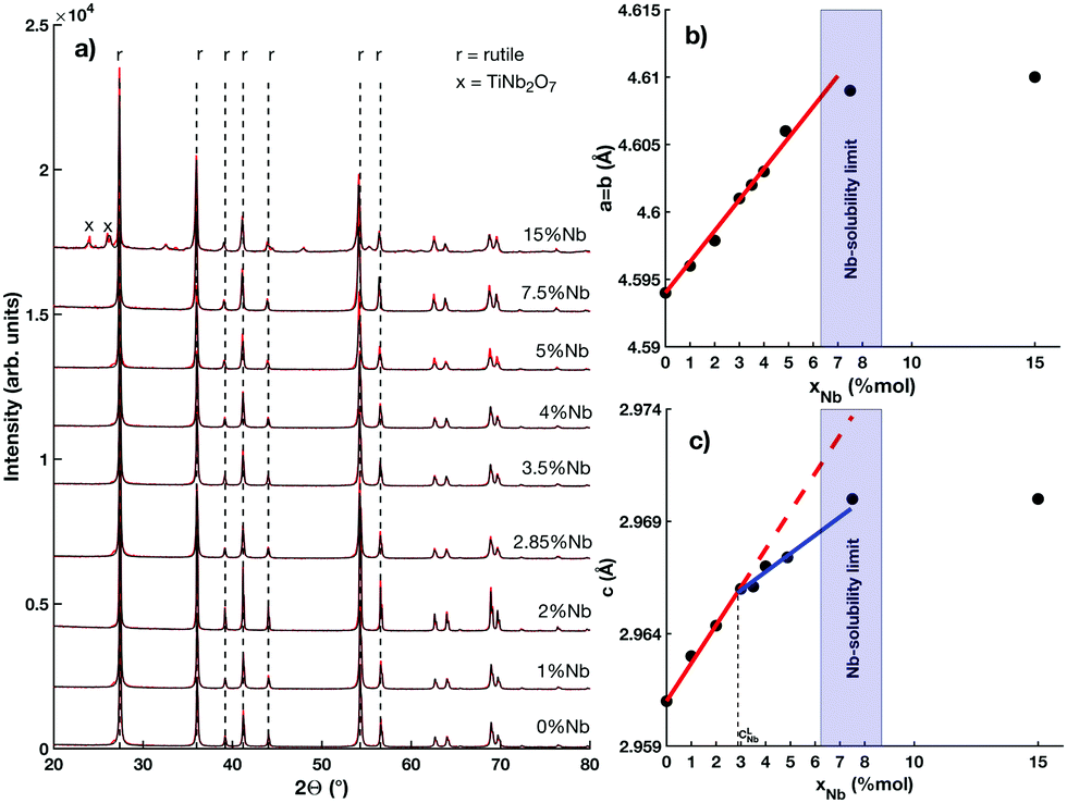 | ||
| Fig. 2 (a) Powder X-ray diffraction patterns (red points) and calculated profiles (solid black lines), obtained after Rietveld refinements, from the bulk of the Ti1−xNbxO2 pellets. The vertical black dotted lines indicate the main reflection positions of the rutile phase (r). The crosses show the TiNb2O7 phase. (b and c) Lattice parameters a (in panel b) and c (in panel c) as a function of the Nb content (black points). The limit of solubility of Nb is shown by the blue rectangle whose width indicates the position uncertainty. Solid lines are linear fits using the Vegard's law (see text). A discontinuity in the Nb dependence of the lattice parameter c is observed at cLNb. | ||
In the following section, the TE properties of the Ti1−xNbxO2 pellets are reported as a function of the Nb content, below the solubility limit (i.e. x < 7.5 mol%), and as a function of temperature, from room temperature to ∼900 K. The results are mostly shown for pellets sintered at 1123 K with the smallest grain size.
The temperature dependences of the electrical conductivity and the Seebeck coefficient obtained from room temperature to ∼900 K are reported in the Fig. 3a and b, respectively. For all specimens, the electrical conductivity decreases linearly as a function of temperature in the log(σT) vs. 1/T representation. For x = 2.8, 4 and 5%, log(σT) is well fitted by using one single slope over the whole temperature range while, for the lower doping levels (x = 1, 2%), two linear regimes are observed with a transition at about 650 K. The linear decrease of log(σT) as a function of 1/T indicates an effect of localization of the charge carriers whose transport is mostly thermally activated. Its temperature dependence is described by the general formula  , where Ea represents the main energy barrier in the system and A a constant which depends on the carrier concentration, i.e. the Nb content. In literature, the electronic localization in conducting TiO2 has been ascribed to the polaronic nature of the conducting Ti3+ states, so that the elementary charge carriers are composites made of self-trapped carrier surrounded by a pattern of atomic displacements. In the Holstein small-polaron model, the activation energy corresponds to the binding potential of the conducting electrons bound to Ti3+ cations and A is a constant which depends on their concentration (i.e. related to the Nb content), the hopping probability and the averaged energy of the optical phonons interacting with electrons.66 In the inset of the Fig. 3a, Ea obtained from the least-squares linear fits of log(σT) versus 1/T in the high-temperature regime (T > 650 K) are reported as a function of the Nb content. The main effect observed is a sharp discontinuity at a Nb content x ∼ 3% which corresponds to a sudden increase of Ea from about 60 meV to 220 meV. The Nb content at which this discontinuity appears is close to cLNb where the structural anomaly on the lattice parameter c is observed (see Fig. 2c). For x< cLNb, Ea increases slightly with the Nb content while the material is getting more metallic which might be an indication of electronic correlations. As shown in the Fig. 3b, the Seebeck coefficient is negative for all Nb contents and over the whole temperature range with values ranging from −500 μV K−1 to −350 μV K−1 in agreement with the previous reports on Nb-doped TiO2.67,68 This indicates that electrons are the major carriers. The Seebeck can be expressed as the sum of two terms S(T) = S1 + S2(T), the first term is temperature independent while the second contains the temperature effects. Both terms depend on the carrier concentration. The Seebeck coefficient changes slightly by about 10–20% over the whole temperature range, so that the term S1 dominates, which indicates that the amount of charge carriers is mostly independent of the temperature. S2(T) follows a C(1/T)n law in the entire temperature range, where C is a constant which depends on the charge carrier concentration and contains a term in energy characterizing the polaronic band. The solid lines in the Fig. 3b show the (Ec/T)n fits for each Nb contents and for temperatures higher than 500 K. Taking into account the experimental uncertainties, the values of n lie in the range [1.5:1.8]. The fitting values of the constant C are reported in the inset of the Fig. 3b. As observed in the Nb dependence of Ea (see inset of Fig. 3a), the Ec(x) exhibits a sharp discontinuity at a Nb concentration of about 3% also close to cLNb.
 | ||
Fig. 3 Temperature dependences of the electrical conductivity (σ) and the Seebeck coefficient (S) in the Ti1−xNbxO2 pellets sintered at 1123 K:  : Ti0.99Nb0.01O2; +: Ti0.98Nb0.02O2; : Ti0.99Nb0.01O2; +: Ti0.98Nb0.02O2;  : Ti0.972Nb0.028O2; : Ti0.972Nb0.028O2;  : Ti0.96Nb0.04O2; : Ti0.96Nb0.04O2;  : Ti0.95Nb0.05O2. (a) log(σT) versus 103/T. The solid lines correspond to the best-fit curves according to Mott's model (see text). (b) Seebeck coefficient as a function of 103/T. The solid lines correspond to the best-fit curves using the Heikes formula. The insets in panels (a and b) show respectively the Nb dependences of the activation energy (Ea) and the constant C (see text). : Ti0.95Nb0.05O2. (a) log(σT) versus 103/T. The solid lines correspond to the best-fit curves according to Mott's model (see text). (b) Seebeck coefficient as a function of 103/T. The solid lines correspond to the best-fit curves using the Heikes formula. The insets in panels (a and b) show respectively the Nb dependences of the activation energy (Ea) and the constant C (see text). | ||
The Nb dependences of σ, S and the TE power factor (S2σ) measured at 800 K in Ti1−xNbxO2 pellets sintered at 1123 K are reported in the Fig. 4a–c, respectively. All these quantities exhibit a pronounced optimum at x ∼ 3% very close to the cLNb (see Fig. 2c). The electrical conductivity first increases linearly for x < cLNb (solid red line in panel a) and then decreases at higher Nb contents. The maximum electrical conductivity at 800 K obtained for x = 2.85% is about 1960 S m−1 in the range of the values measured in polycrystalline38,42,69 and in single crystals Ti1−xNbxO2.45 The increase in the electrical conductivity with respect to the Nb content for x < cLNb is consistent with previous reports where it was found that Nb4+ cations act as a simple electron donors in this doping range.5,6,25,38,40–45 Concomitantly, the absolute value of the Seebeck coefficient decreases for x < cLNb and then increases for higher Nb content with a minimum value of −370 μV K−1 for x = 2.85%. For x ≲ cLNb, the Nb dependence of the Seebeck coefficient follows the Heikes formula, that is  (solid red line in panel b). Overall, the temperature and Nb dependences of the Seebeck coefficient are consistent with the formula of the polaronic Seebeck derived by Emin.70 In the high temperature and low doping range of this theory, the polaronic Seebeck simplifies into the sum of two terms: a first contribution which is given by the Heikes formula, and a second contribution which contains the temperature effect. The latter follows a power law
 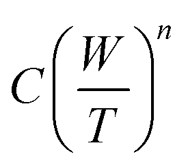 with n = 2, where W represents the width in energy of the polaronic band and C is a constant which depends on the charge carrier concentration. In this context, the sudden increase of the constant C in S2(T) observed at cLNb (see inset in Fig. 3b) may arise from the broadening of the polaronic band due to the addition of defect states with the formation of the Nb–Nb dimers. The TE power factor reaches an optimal value of 250 μW m−1 K−2 for x ∼ cLNb. This value is in the middle range of the power factors measured in TM oxides71,72 but is still one order of magnitude lower than those observed in efficient TE materials due to the low electrical conductivity.73 Further improvement of the TE power factor in Ti1−xNbxO2 will need to explore either a dual doping in addition to Nb or oxygen reduction. In the above considerations, the effect on the electrical properties of the crystalline domain size, the grain size, the grain boundaries and micro-strains have not been considered, although they are known to impact significantly.74,75 The difficulty lies in the fact that the change of the sintering conditions used to reduce the average grain size might also slightly change the amount of oxygen in the materials, thus hindering the intrinsic effect of the grain size. Further study of the particle size dependence on the electrical transport in bulk nanostructured r-TiO2 with a fine control over the oxygen content would be required in particular when lower particle size will be accessible.
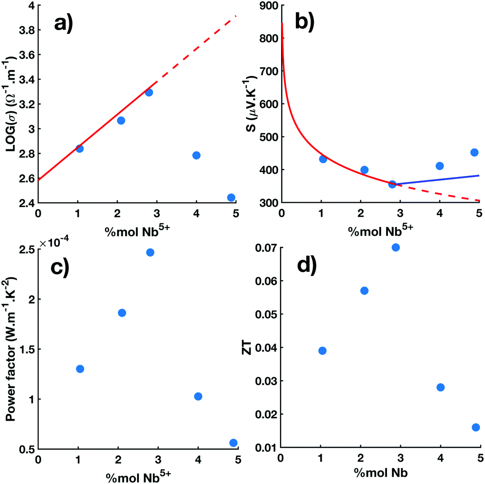 | ||
| Fig. 4 Nb dependences of the electrical conductivity (log(σ)) in panel (a), the Seebeck coefficient (S) in panel (b), the thermoelectric power factor (σS2) in panel (c) and the figure of merit (ZT) in panel (d) obtained at 800 K in the Ti1−xNbxO2 pellets. Measurements are reported in pellets of Ti1−xNbxO2 sintered at 1123 K (blue filled circles). All quantities exhibit an optimum at xNb ∼ cLNb (see Fig. 2c). For x < cLNb, the solid red lines correspond to the fit with the polaronic transport model (see text) whose carrier content is directly given by the Nb content. The solid lines are continued by dotted lines beyond cLNb. For x > cLNb, the solid blue lines show the model with a reduced charge carrier content due to the formation of Nb dimers (see text). | ||
As described above and shown in the Fig. 4, the Nb-dependences of σ, S exhibit an optimum at about cLNb ∼ 3% in the [300 K: 900 K] temperature range. This effect on the electrical properties correlates with the structural anomaly observed in the Nb-dependence of the lattice parameter c of the tetragonal unit cell (see Fig. 2c).
Such anomaly on the electronic and structural properties of TiO2 with the incorporation of Nb has already been reported at room temperature in single crystals and bulk polycrystals for similar Nb content of about 2–3%. The Nb dependence in the electrical properties of nanocrystalline thin films of anatase Nb-TiO2 exhibits similar discontinuity with a first strong decrease of the resistivity in the range lower than 2% followed by a plateau in the range 2–6% of Nb doping.39 Different scenarios were suggested to explain why, above a few percent, the Nb ion doesn't act as a simple electron donor. One is the formation of short Nb–Nb dimers as introduced above.21,38,41,43,45 An alternative scenario is the segregation of the Nb ions at the grain boundaries so that they don't provide any additional charge carrier but act as carrier scattering centers damaging the electrical conduction.39 Other research has suggested that the delocalized electron added by Nb in TiO2 can be pinned on oxygen vacancy resulting in defect dipoles.25 Some research has suggested Nb–Ti hybridization forms a nonbonding band near the valence band.59 In our case, we found simultaneously a structural and electrical discontinuities at the same Nb content at cLNb and then a decrease in the electrical conductivity for a Nb content higher then cLNb which underlays a carrier annihilation effect induced by these additional Nb ions. Moreover there is no fingerprint for a segregation of Nb in the diffraction spectra. Viewed in their entirety, our data favour the scenario of the Nb–Nb dimer formation. In a first approximation, for x ≳ cLNb, the main consequence of the Nb dimer formation is the reduction of the charge carrier content. By considering the deviation of the Nb-dependence of the lattice parameter c for x ≳ cLNb from its linear increase observed at lower doping (see Fig. 2c), we quantify the amount of Nb dimers and, thus, the reduced charge carrier content in the system (see ESI†). In the following, we use the later in order to extrapolate the Nb-dependences of σ and S, observed for x ≲ cLNb at 800 K, in the region where x ≳ cLNb. In panel (b) of Fig. 4 (solid blue line), the Nb-dependence of the Seebeck coefficient, obtained from the Heikes formula with the reduced charge content, is shown for x ≳ cLNb. Although it slightly underestimates the absolute value of the Seebeck coefficient, by about 10–20%, this simple approach allows to reproduce the upturn observed at cLNb. It works probably because the Seebeck is almost temperature independent (S2 ≫ S1) and depends mostly on the charge carrier content. On the other hand, the upturn of the electrical conductivity observed at cLNb and its abrupt decrease for x ≳ cLNb, see Fig. 4a, can not be reproduced by considering only the decrease of the charge carrier content. This effect together with the sudden increase at cLNb of the activation energy, shown in the inset of Fig. 3a, indicates a deep change in the hopping mechanism with the formation of Nb–Nb dimers which corroborates the reduction of the electron mobility reported in the Hall effect measurements.45 It, therefore, indicates that Nb dimers play a prominent role in the electronic transport.
The lattice thermal conductivity, λl, measured in the pellets of Ti1−xNbxO2 from room temperature to 900 K are reported in Fig. 5a.
 | ||
Fig. 5 (a) Temperature dependences of the lattice thermal conductivity, λL, in the series of Ti1−xNbxO2 samples. ( : bulk TiO2 from U. Diebold et al.;76 ■: Ti0.99Nb0.01O2 with grain size of 2 μm from Zaitev et al.41 : bulk TiO2 from U. Diebold et al.;76 ■: Ti0.99Nb0.01O2 with grain size of 2 μm from Zaitev et al.41 : Ti0.99Nb0.01O2 at 1123 K; : Ti0.99Nb0.01O2 at 1123 K;  : Ti0.98Nb0.02O2 at 1123 K; : Ti0.98Nb0.02O2 at 1123 K;  : Ti0.98Nb0.02O2 at 1233 K; : Ti0.98Nb0.02O2 at 1233 K;  : Ti0.972Nb0.028O2 at 1123 K; : Ti0.972Nb0.028O2 at 1123 K;  : Ti0.97Nb0.03O2 at 1123 K; : Ti0.97Nb0.03O2 at 1123 K;  : Ti0.95Nb0.05O2 at 1123 K), (b) inverse of the lattice thermal conductivity normalized to the value in pure TiO2 as a function of the inverse grain size derived from SEM pictures, see Fig. 1. ( : Ti0.95Nb0.05O2 at 1123 K), (b) inverse of the lattice thermal conductivity normalized to the value in pure TiO2 as a function of the inverse grain size derived from SEM pictures, see Fig. 1. ( : Ti0.98Nb0.02O2 at 373 K and his linear fit (y = 147.3x + 1.003) including the point from Zaitev et al.41 (■); : Ti0.98Nb0.02O2 at 373 K and his linear fit (y = 147.3x + 1.003) including the point from Zaitev et al.41 (■);  : Ti0.965Nb0.035O2 at 373 K and his linear fit (y = 174.1x + 1.02); : Ti0.965Nb0.035O2 at 373 K and his linear fit (y = 174.1x + 1.02);  : the skutterudite In0.25Co4Sb12 at 300 K from Benyahia et al.77 and linear fit (y = 70.3x + 1.044)). : the skutterudite In0.25Co4Sb12 at 300 K from Benyahia et al.77 and linear fit (y = 70.3x + 1.044)). | ||
λ
l was deduced by subtracting the electronic carrier contribution to the measurement of the total thermal conductivity which, as estimated from the Weidemann–Franz law, doesn't exceed 2% of it, so that the thermal conduction is mostly dominated by the lattice (see Fig. S3 in the ESI†). The room temperature value of λl in polycrystalline TiO2 is typically of ∼7 W m−1 K−1 and monotonically decreases with temperature as reported in Fig. 5a.76 The room temperature value of λl in our nanostructured ceramics of TiO2 is on an average of about ∼3.5 W m−1 K−1 independently of the Nb content. This value is about two times lower than that measured in the bulk TiO2. As a function of temperature, λl shows a slight decrease, much less pronounced than the one in bulk TiO2, and reaches values between 2.5–3 W m−1 K−1 at the high limit of the temperature range. The measurement of λl(T) is also reported for the pellet of Ti1−xNbxO2 (with x = 2.85%) sintered at 1233 K in Fig. 5a (empty blue circles). λl(T) exhibits a clear dependence on the grain size. The influence of the grain size (D) on the lattice thermal conductivity (λl) can be quantified by using the model of Nan and Birringer,78 with the correction of Yang.79 This model relates the inverse of λl to the inverse of the grain size (D):  with λL0 the lattice thermal conductivity in single crystal (D → ∞) and LK the Kapitza length. In Fig. 5b, the inverse of λl normalized to the bulk value (λl0) is represented against the inverse of the average grain size diameter (1/D) in two pellets of Ti1−xNbxO2 for x = 0.02 and 0.035. It confirms that
  is linear with respect to
 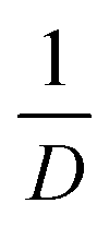 . The fit using the function of Nan and Birringer yields a Kapitza length LK ≈ 156 nm. Similar measurements recently obtained in the skutterudite In0.25Co4Sb12, reported in Fig. 5a, also show a linear relation between λl and D. However, the Kapiza length is significantly higher (about a factor of two) in TiO2 than in the skutterudite, meaning that the decrease of the grain size is more efficient to reduce λl in TiO2. From the fit, we can estimate that a pellet of TiO2 with a grain size of about 25 nm would have a lattice thermal conductivity lower than 1 W m−1 K−1. The bulk phonon spectrum is fundamentally different between the skutterudite and TiO2. Indeed, in the later, the phase space in momentum and in energy available for acoustic phonons, which are assumed to be the dominant heat carriers, as well as the group velocities near the center of the Brillouin zone are larger than in the skutterudite which might explain the higher sensitivity of TiO2 against the nanostructuration.80–82
4 Conclusions
In conclusion, the thermoelectric properties of nanostructured Ti1−xNbxO2 pellets in the low doping range and below the Nb solubility limit, found at about x ∼7.5%, have been measured from room temperature to 900 K. Firstly, we have shown the existence of an optimum in the Nb dependences of the electrical conductivity, the Seebeck coefficient and the thermoelectric power factor which appears for a Nb content of about cLNb ∼ 2.85% (well below the Nb solubility limit in rutile). This optimal concentration in the Nb dependence of the electronic properties correlates with a structural anomaly observed in the Nb dependence of the lattice parameter c. Similarly reported at room temperature in bulk Nb-doped TiO2, this optimal Nb content is related to the formation of Nb–Nb dimers. Below the optimal concentration, the electrical conductivity increases and the absolute value of the Seebeck coefficient decreases upon adding Nb4+ cations which act as electron donors. The transport mechanism is dominated by hopping processes which is characterized by an activation energy of about 70 meV. At higher doping level, an upturn is observed in the Nb-dependences of the electrical conductivity and the Seebeck coefficient, so that the electrical conductivity decrease and the absolute value of the Seebeck coefficient increase. The changes in the Seebeck is almost reproduced by considering the reduction of the charge carrier content with the appearance of Nb dimers. On the other hand, the electronic conductivity is still dominated by hopping processes but with a much larger activation energy of about 200 meV, indicating that the Nb dimers play a role in the electronic transport beyond the simple annihilation of charge carriers. The optimal value of the TE figure of merit, ZT, obtained at the optimal Nb content in the pellets with the minimum grain size is of about 0.08 at 873 K. Secondly, the thermal measurements in pellets with an averaged grain size of 300 nm and 170 nm have revealed a significant decrease of the lattice thermal conductivity with the grain size diameter following the model established by Nan and Beringer. Thus, lowering the grain size down to 170 nm has allowed to reduce the lattice thermal conductivity of rutile by almost a factor of two. This grain size dependence of λl in TiO2 is much larger than the one observed in complex intermetallic thermoelectric materials. Further improvement of the ZT may be achieved by decreasing further the grain size below 170 nm and by exploring the dual doping. The appearance of the Nb dimers changes abruptly the electronic properties of rutile TiO2 and introduces large defects structure in the system which may open an opportunity to reduce more the thermal conduction.Conflicts of interest
There are no conflicts to declare.Acknowledgements
This work was supported by the LABEX iMUST (ANR-10-LABX-0064 project OTHELLO) of Université de Lyon, within the program “Investissements d'Avenir” (ANR-11-IDEX-0007) operated by the French National Research Agency (ANR). SP acknowledges the Lyon IDEX Scientific Breakthrough program for funding of the project IPPON. The authors thank the technological platforms PLECE@ILMTech, TRANSPORT@ILMTech and MATEIS@INSA-Lyon. The authors would like to thank V. Giordano, S. Vignoli, S. Thébaud, C. Adessi and G. Bouzerar for fruitful discussions. We also thank R. Chiriac and F. Toche for the TG-DTA analyzes carried out at the platform Plateforme Lyonnaise d'Analyses Thermiques.Notes and references
- A. Fujishima, X. Zhang and D. A. Tryk, Surf. Sci. Rep., 2008, 63, 515 CrossRef CAS.
- K. Nakata and A. Fujishima, J. Photochem. Photobiol., C, 2012, 13, 169–189 CrossRef CAS.
- S. U. M. Khan, M. Al-Shahry and W. B. Ingler Jr., Science, 2002, 297, 2243–2245 CrossRef CAS PubMed.
- H. Sohn, S. Kim, W. Shin, J. M. Lee, H. Lee, D. J. Yun, K. S. Moon, I. T. Han, C. Kwak and S. J. Hwang, ACS Appl. Mater. Interfaces, 2018, 10, 2688–2700 CrossRef CAS PubMed.
- T. Hitosugi, N. Yamada, S. Nakao, Y. Hirose and T. Hasegawa, Phys. Status Solidi A, 2010, 207, 1529–1537 CrossRef CAS.
- Y. Furubayashi, T. Hitosugi, Y. Yamamoto, K. Inaba, G. Kinoda, Y. Hirose, T. Shimada and T. Hasegawa, Appl. Phys. Lett., 2005, 86, 252101 CrossRef.
- D. B. Strukov, G. S. Snider, D. R. Stewart and R. S. Williams, Nature, 2008, 453, 80–83 CrossRef CAS PubMed.
- Z. Li, Z. Yao, A. A. Haidry, T. Plecenik, L. Xie, L. Sun and Q. Fatima, Int. J. Hydrogen Energy, 2018, 43, 21114–21132 CrossRef CAS.
- M. Madian, A. Eychmüller and L. Giebeler, Batteries, 2018, 4, 1–36 CrossRef.
- Z. Yuan, J. Gong, S. Xu, Z. Li and G. Tang, J. Alloys Compd., 2017, 710, 778–783 CrossRef CAS.
- G. Kieslich, G. Cerretti, I. Veremchuk, R. P. Hermann, M. Panthöfer, J. Grin and W. Tremel, Phys. Status Solidi A, 2016, 213, 808–823 CrossRef CAS.
- J. W. Fergus, J. Eur. Ceram. Soc., 2012, 32, 525–540 CrossRef CAS.
- G. J. Snyder and E. S. Toberer, Nat. Mater., 2008, 7, 105–114 CrossRef CAS PubMed.
- J. Tang, W. Wang, G. L. Zhao and Q. Li, J. Phys.: Condens. Matter, 2009, 21, 205703 CrossRef PubMed.
- J. Muscat, V. Swamy and N. M. Harrison, Phys. Rev. B: Condens. Matter Mater. Phys., 2002, 65, 224112 CrossRef.
- H. Zhang and J. F. Banfield, J. Phys. Chem. B, 2000, 104, 3481–3487 CrossRef CAS.
- D. Machon, M. Daniel, P. Bouvier, S. Daniele, S. L. Floch, P. Melinon and V. Pischedda, J. Phys. Chem. C, 2011, 115, 22286–22291 CrossRef CAS.
- F. Lechermann, W. Heckel, O. Kristanovski and S. Müller, Phys. Rev. B: Condens. Matter Mater. Phys., 2017, 95, 195159 CrossRef.
- C. Di Valentin, G. Pacchioni and A. Selloni, J. Phys. Chem. C, 2009, 113, 20543–20552 CrossRef CAS.
- D. O. Scanlon, C. W. Dunnill, J. Buckeridge, A. J. L. Stephen, A. Shevlin, S. M. Woodley, C. R. A. Catlow, M. J. Powell, R. G. Palgrave, I. P. Parkin, G. W. Watson, T. W. Keal, P. Sherwood, A. Walsh and A. A. Sokol, Nat. Mater., 2013, 12, 798–801 CrossRef CAS PubMed.
- D. Morris, Y. Dou, J. Rebane, C. E. J. Mitchell, R. G. Egdell, D. S. L. Law and M. Casarin, Phys. Rev. B: Condens. Matter Mater. Phys., 2000, 61, 13445–13457 CrossRef CAS.
- Y. Tezuka, S. Shin, T. Ishii, T. Ejima, S. Suzuki and S. Sato, J. Phys. Soc. Jpn., 1994, 63, 347–357 CrossRef CAS.
- P. J. Hardman, G. N. Raikar, C. A. Muryn, G. van der Laan, P. L. Wincott, G. Thornton, D. W. Bullett and P. A. D. M. A. Dale, Phys. Rev. B: Condens. Matter Mater. Phys., 1994, 49, 7170–7177 CrossRef CAS PubMed.
- D. C. Cronemeyer, Phys. Rev., 1952, 87, 876–886 CrossRef CAS.
- L. Zhao, J. Wang, Z. Gai, J. Li, J. Liu, J. Wang, C. Wang and X. Wang, RSC Adv., 2019, 9, 8364–8368 RSC.
- L. Chiodo, J. M. García-Lastra, A. Iacomino, S. Ossicini, J. Zhao, H. Petek and A. Rubio, Phys. Rev. B: Condens. Matter Mater. Phys., 2010, 82, 045207 CrossRef.
- S. Thébaud, C. Adessi, S. Pailhès and G. Bouzerar, Phys. Rev. B: Condens. Matter Mater. Phys., 2017, 96, 075201 CrossRef.
- I. Tsuyumoto, T. Hosono and M. Murata, J. Am. Ceram. Soc., 2006, 89, 2301–2303 CAS.
- N. Okinaka and T. Akiyama, Jpn. J. Appl. Phys., 2006, 45, 7009–7010 CrossRef CAS.
- Q. He, Q. Hao, G. Chen, B. Poudel, X. Wang, D. Wang and Z. Ren, Appl. Phys. Lett., 2007, 91, 052505 CrossRef.
- A. Bentien, S. Johnsen, G. K. H. Madsen, B. B. Iversen and F. Steglich, Europhys. Lett., 2007, 80, 17008 CrossRef.
- S. J. Pandey, G. Joshi, S. Wang, S. Curtarolo and R. M. Gaume, J. Electron. Mater., 2016, 45, 5526–5532 CrossRef CAS.
- D. Portehault, V. Maneeratana, C. Candolfi, N. Oeschler, I. Veremchuk, Y. Grin, C. Sanchez and M. Antonietti, ACS Nano, 2011, 5, 9052–9061 CrossRef CAS PubMed.
- K. Song, X. Han and G. Shao, J. Alloys Compd., 2013, 551, 118–124 CrossRef CAS.
- T. Yamamoto and T. Ohno, Phys. Rev. B: Condens. Matter Mater. Phys., 2012, 85, 033104 CrossRef.
- M. R. Antonio, I. Song and H. Yamada, J. Solid State Chem., 1991, 93, 183–192 CrossRef CAS.
- B. Poumellec, F. Lagnel, J. F. Marucco and B. Touzelin, Phys. Status Solidi B, 1986, 133, 371–377 CrossRef CAS.
- G. Sahasrabudhe, J. Krizan, S. L. Bergman, R. J. Cava and J. Schwartz, Chem. Mater., 2016, 28, 3630–3633 CrossRef CAS.
- J. Liu, X. Zhao, L. Duan, M. Cao, H. Sun, J. Shao, S. Chen, H. Xie, X. Chang and C. Chen, Appl. Surf. Sci., 2011, 257, 10156–10160 CrossRef CAS.
- L. R. Sheppard, T. Bak and J. Nowotny, Phys. Status Solidi A, 2006, 203, R85–R87 CrossRef CAS.
- S. V. Zaitsev, J. Moon, H. Takagi and M. Awano, Adv. Powder Technol., 2000, 11, 211–220 CrossRef CAS.
- B. Poumellec, J. F. Marucco and F. Lagnel, J. Phys. Chem. Solids, 1986, 47, 381–385 CrossRef CAS.
- J. F. Baumard and E. Tani, J. Chem. Phys., 1977, 67, 857–860 CrossRef CAS.
- K. Sakata, I. Nishida, M. Matsushima and T. Sakata, J. Phys. Soc. Jpn., 1969, 27, 506 CrossRef CAS.
- M. Itakura, N. Niizeki, H. Toyoda and H. Iwasaki, Jpn. J. Appl. Phys. (1962–1981), 1967, 6, 311–317 CrossRef CAS.
- G. Kolesov, B. A. Kolesov and E. Kaxiras, Phys. Rev. B: Condens. Matter Mater. Phys., 2017, 96, 195165 CrossRef.
- A. Kazempour, Phys. Scr., 2015, 90, 025804 CrossRef.
- B. J. Morgan, D. O. Scanlon and G. W. Watson, J. Mater. Chem., 2009, 19, 5175–5178 RSC.
- E. Hendry, F. Wang, J. Shan, T. F. Heinz and M. Bonn, Phys. Rev. B: Condens. Matter Mater. Phys., 2004, 69, 081101 CrossRef.
- R. G. Breckenridge and W. R. Hosler, Phys. Rev., 1953, 91, 793–802 CrossRef CAS.
- A. A. Bolzan, C. Fong, B. J. Kennedy and C. J. Howard, J. Solid State Chem., 1994, 113, 9–14 CrossRef CAS.
- S. M. Shapiro, J. D. Axe, G. Shirane and P. M. Raccah, Solid State Commun., 1974, 15, 377–381 CrossRef CAS.
- T. Sakata, K. Sakata and I. Nishida, Phys. Status Solidi B, 1967, 20, K155–K157 CrossRef CAS.
- R. F. Janninck and D. H. Whitmore, J. Phys. Chem. Solids, 1966, 27, 1183–1187 CrossRef CAS.
- A. O'Hara and A. A. Demkov, Phys. Rev. B: Condens. Matter Mater. Phys., 2015, 91, 094305 CrossRef.
- A. O'Hara, T. N. Nunley, A. B. Posadas, S. Zollner and A. A. Demkov, J. Appl. Phys., 2014, 116, 213705 CrossRef.
- W. Rudorff and H.-H. Luginsland, Z. Anorg. Allg. Chem., 1964, 334, 125–141 CrossRef.
- A. E. Shimabukuro, A. Ishii, I. Oikawa, Y. Yamazaki, M. Imura, T. Kanai, F. S. Ohuchi and H. Takamura, Appl. Surf. Sci., 2019, 464, 61–67 CrossRef CAS.
- S. Chambers, Y. Gao, Y. Kim, M. Henderson, S. Thevuthasan, S. Wen and K. Merkle, Surf. Sci., 1996, 365, 625–637 CrossRef CAS.
- A. A. Ogacho, P. Ajuoga and B. O. Aduda, Int. J. Innovation Educ. Res., 2015, 3, 140–146 Search PubMed.
- K. Morita, B.-N. Kim, H. Yoshida, K. Hiraga and Y. Sakka, Acta Mater., 2015, 84, 9–19 CrossRef CAS.
- J. Rodriguez-Carvajal, IUCr Newslett., 2001, 26, 12–19 Search PubMed.
- Y. Lu, M. Hirohashi and K. Sato, Mater. Trans., 2006, 46, 1449–1452 CrossRef.
- T. G. Babich, A. V. Zagorodnyuk, G. A. Teterin, M. Y. Khodos and A. P. Zhirnova, Russ. J. Inorg. Chem., 1988, 33, 560–563 Search PubMed.
- K. Sakata, J. Phys. Soc. Jpn., 1969, 26, 582 CrossRef CAS.
- A. J. Bosman and H. J. Van Daal, Adv. Phys., 1970, 19, 1–117 CrossRef CAS.
- H. P. R. Frederikse, J. Appl. Phys., 1961, 32, 2211–2215 CrossRef CAS.
- J. F. Baumard and E. Tani, Phys. Status Solidi A, 1977, 39, 373–382 CrossRef CAS.
- C. Liu, L. Miao, D. Hu, R. Huang, C. A. J. Fisher, S. Tanemura and H. Gu, Phys. Rev. B: Condens. Matter Mater. Phys., 2013, 88, 205201 CrossRef.
- D. Emin, J. Appl. Phys., 2016, 119, 045101 CrossRef.
- K. Koumoto, Y. Wang, R. Zhang, A. Kosuga and R. Funahashi, Annu. Rev. Mater. Res., 2010, 40, 363–394 CrossRef CAS.
- H. Ohta, Mater. Today, 2007, 10, 44–49 CrossRef CAS.
- A. M. Dehkordi, M. Zebarjadi, J. He and T. M. Tritt, Mater. Sci. Eng., 2015, 97, 1–22 CrossRef.
- A. Goktas, A. Tumbul, Z. Aba and M. Durgun, Thin Solid Films, 2019, 680, 20–30 CrossRef CAS.
- K. Safeen, V. Micheli, R. Bartali, G. Gottardi, A. Safeen, H. Ullah and N. Laidani, Mod. Phys. Lett. B, 2019, 33, 1950313 CrossRef CAS.
- U. Diebold, Surf. Sci. Rep., 2003, 48, 53–229 CrossRef CAS.
- M. Benyahia, V. Ohorodniichuk, E. Leroy, A. Dauscher, B. Lenoir and E. Alleno, J. Alloys Compd., 2018, 735, 1096–1104 CrossRef CAS.
- C.-W. Nan and R. Birringer, Phys. Rev. B: Condens. Matter Mater. Phys., 1998, 57, 8264–8268 CrossRef CAS.
- H.-S. Yang, G. R. Bai, L. J. Thompson and J. A. Eastman, Acta Mater., 2002, 50, 2309–2317 CrossRef CAS.
- S. Pailhès, H. Euchner, V. Giordano, R. Debord, A. Assy, S. Gomès, A. Bosak, D. Machon, S. Paschen and M. de Boissieu, Phys. Rev. Lett., 2014, 113, 025506 CrossRef PubMed.
- H. Euchner, S. Pailhès, L. T. K. Nguyen, W. Assmus, F. Ritter, A. Haghighirad, Y. Grin, S. Paschen and M. de Boissieu, Phys. Rev. B: Condens. Matter Mater. Phys., 2012, 86, 224303 CrossRef.
- P.-F. Lory, S. Pailhès, V. M. Giordano, H. Euchner, H. D. Nguyen, R. Ramlau, H. Borrmann, M. Schmidt, M. Baitinger, M. Ikeda, P. Tomeš, M. Mihalkovic, C. Allio, M. R. Johnson, H. Schober, Y. Sidis, F. Bourdarot, L. P. Regnault, J. Ollivier, S. Paschen, Y. Grin and M. de Boissieu, Nat. Commun., 2017, 8, 491 CrossRef PubMed.
Footnote |
| † Electronic supplementary information (ESI) available: Determination of the amount of dimer, TGA and TDA curves of the as-prepared powder, SEM images and elemental mapping of a TiO2 pellet doped with 2 mol% of niobium after sintering at 1233 K, electronic thermal conductivities of the Ti0.972Nb0.028O2 pellet sintered at 1123 K according to the Wiedemann–Franz law. See DOI: 10.1039/d0cp00652a |
| This journal is © the Owner Societies 2020 |