Quantitative characterization of silicon solar cells in the electro-analytical approach: Combined measurements of temperature and voltage dependent electrical parameters†
D. J.
Crain
,
J. E.
Garland
,
S. E.
Rock
and
D.
Roy
*
Department of Physics, Clarkson University, Potsdam, NY 13699-5820, USA. E-mail: samoy@clarkson.edu; Fax: +1-315-268-6610; Tel: +1-315-268-6676
First published on 11th October 2011
Abstract
Electrochemical and photo-electrochemical systems, often involving solid-liquid interfaces, have traditionally dominated the field of material/device characterization using electro-analytical tools such as linear sweep voltammetry (LSV) and impedance spectroscopy (IS). Recent developments in these measurement techniques have broadened their applications to various studies of non-electrochemical solid state systems. The present work provides further experimental illustration of these latter utilities of LSV and IS through a detailed study of the temperature and voltage sensitive features of the minority carrier lifetime, series resistance and back surface field (BSF) parameters of a mono-crystalline Si solar cell. Apart from displaying their characteristic temperature dependencies, the measured parameters respond to variations in the cell voltage, and exhibit certain mutually interacting features of the observed effects. The results also demonstrate how the characteristic features of charge recombination in the quasi-neutral and space charge regions of the solar cell can be resolved with D.C. voltage dependent A.C. impedance measurements.
1. Introduction
Traditional applications of the electro-analytical techniques of impedance spectroscopy (IS) and linear sweep voltammetry (LSV) have frequently centered on solid-liquid electrochemical interfaces.1 A natural extension of these techniques has also emerged through the last decade in various studies of novel photo-electrochemical systems like dye sensitized solar cells.2,3 In comparison, the utility of these electrochemical techniques has remained somewhat underexplored in similar studies of solid state photovoltaic devices.4–6 Quantitative applications of combined IS and LSV in the latter field have been demonstrated lately for the characterization of Si based solar cells.7–11 Although the essential elements of the A.C. perturbation (small-signal) approach have been employed in earlier studies of Si solar cells,12–14 more formal protocols of IS, especially those of complex nonlinear least square (CNLS) analysis have been implemented recently in the electro-analytical framework of solar cell characterization.7–9 Based on these developments, the combination of LSV with IS can provide an integrated approach to simultaneous measurements of both the D.C. and the A.C. parameters of solar cells. This experimental strategy can allow for the collection of large amounts of data within a reasonable timeframe, and can facilitate the investigation of various previously unexplored fundamental and applied aspects of a range of photovoltaic processes.Under a D.C. bias, different electrical features of a solar cell are governed by different sets of device parameters that can be sampled in a voltage selective mode. For instance, under reverse bias (RB) and moderate forward bias (FB), the space charge region (SCR) capacitance and the shunt resistance of the cell dominate the cell's impedance response. Similarly, the effects of the SCR-localized charge recombination and those of diffusion/recombination in the quasi-neutral regions typically are manifested at moderate and strong FB voltages, respectively.7,8 All these effects are sensitive to temperature variations, and can impact several aspects of cell performance as well as the considerations for optimized coupling of switching regulators.15,16 In the electro-analytical approach, these various effects can be separately examined by probing their voltage selective signature parameters under thermal control. The main experimental framework of this strategy has been recently discussed for Si solar cell characterization at room temperature.7,8 Temperature dependent attributes of certain cell parameters have also been examined in this approach.17 Using a back surface field (BSF) mono-crystalline Si solar cell, the present work illustrates further the electro-analytical platform for combined temperature and voltage dependent measurements of a selected set of device parameters.
Electro-analytical characterization of a Si solar cell typically uses LSV for recording the current–voltage characteristics of the cell. IS measurements are performed at different D.C. bias voltages, where the selection of the experimental voltage range depends on the specific parameters to be characterized.8,17 For instance, the relative effects of charge recombination occurring in the SCR and in the base of a cell can be examined by studying the cell's effective diode ideality factor at moderate RB and FB voltages. The corresponding variations of the SCR capacitance at such voltages provide information about the built-in potential and the acceptor concentration. IS data recorded under these biasing conditions also lead to direct determination of the shunt resistance, as well as the ohmic component of the series resistance.8,18 We have recently reported electro-analytical measurements of these specific parameters for an n+-p-p+Si solar cell that was subjected to variable D.C. bias voltages between −0.6 and 0.3 V and thermally maintained at different temperatures between 15 and 60 °C.17
The present work focuses on a number of parameters that dominate the electrical response of a typical Si solar cell under strong FB (0.4–0.6 V), and examines how they are affected by the variations of voltage and temperature (25–55 °C). These FB-activated device parameters include the diffusion capacitance and diffusion resistance of injected charge carriers, the minority carrier lifetimes, as well as the capacitance, resistance and relaxation time of majority carriers at the p-p+ low-high (LH) junction associated with the BSF of the cell. In addition, the voltage and temperature dependent trends of the cell's series resistance are investigated, focusing particularly on the non-ohmic component of this resistance.
The considerations of cell illumination is an essential aspect of IS based measurements of solar cell parameters. The D.C. circuit model of a dark solar cell changes under illumination upon the introduction of an active element of a current source.19 However, the general A.C. response of a Si solar cell, as characterized in terms of cell equivalent circuit (CEC) models of passive elements, remains essentially unaltered for different cell illuminations at 0–1 Sun.8 This illumination independent behavior of the impedance parameters of a Si solar cell is linked to the observation that, the D.C. voltage drop (Vj) at the n+-p junction and the temperature of the cell predominantly control the values of the passive impedance elements in the device.17
In an illuminated cell, the value of Vj is dictated by photo-generated charge injection, and most internal temperature variations in this case have photo-thermal origins. In a dark cell, charge injection at the n+-p junction is achieved by the application of a FB voltage. As long as the photo-thermal and photovoltaic effects are kept separated through external temperature control, the effects of varying Vj on the cell's impedance parameters exhibit their same signature features, irrespective of the mechanism regulating Vj (illumination or voltage induced charge injection). Due to this reason, the A.C. CEC description of the Si solar cell stays essentially the same between dark and moderately illuminated conditions; however, the values of the individual elements in the CEC change as Vj changes due to variations in the bias voltage and/or cell illumination.8 Based on these considerations, the temperature and voltage dependent electro-analytical measurements are performed in the present work employing a dark cell. The experimental results are analyzed using currently available theoretical treatments, and this provides a framework for addressing certain underexplored aspects of Si solar cell characterization.
2. Experimental
The 2 × 2 cm2 surface area mono-crystalline Si (n+-p-p+) BSF cell, obtained from Newport Oriel (VLSI standards, SRC-1000-TC-QZ), displayed an open circuit voltage (OCV) of 0.61 V with 1 Sun illumination at 25 °C, and had a base width (wb) of about 300 μm. Because this base was significantly thin compared to the electron diffusion length in the p-Si base (∼0.2 mm16), it was possible to effectively utilize the BSF feature of the solar cell. All experiments were performed in a light-tight Faraday cage mounted on an Ealing optical table, while the test cell was maintained under temperature control with a TC 24–10 Peltier thermoelectric device from TE technologies. Fig. 1 schematically shows the main components of the experimental arrangement including the solar simulator. The experiments were performed using a dark cell, and the detailed features of the anti reflection coating (ARC) and the fingers/bus-bars of the cell are excluded from the drawing. The solar cell was mounted on a Flame Retardant Class 4 Printed Circuit Board (FR4-PCB) with a thermally conductive paste. The PCB electrically isolated the back contact of the cell from the Al block used as a thermal mass. A thermocouple was mounted next to the test cell on the copper surface of the PCB to record temperatures. LSV and IS measurements were carried out by using a four terminal Princeton Applied Research Versastat-3 potentiostat. The working electrode (WE) and one of the reference electrodes (RE1) of the potentiostat were connected together to the back contact of the cell. The counter electrode (CE), and the second reference electrode (RE2) was connected to the bus bar/fingers.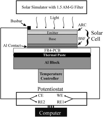 | ||
| Fig. 1 Schematic representation (not drawn to scale) of the experimental arrangement. The components of the cell and the setup are explained in the main text. All experiments reported in this work were performed with an un-illuminated solar cell, and the entire experimental setup was enclosed in a faraday cage. | ||
For LSV, the applied voltage V was scanned at a rate of 5 mV s−1, maintaining the WE terminal at a positive potential with respect to the CE terminal. IS experiments used A.C. perturbation voltages of 5 mV root-mean-square amplitude and 196 frequencies, logarithmically spaced from 5 Hz to 105 KHz. The zero impedance reference of the test setup at the device-under-test insertion point was <30 mΩ at 100 kHz. The recorded IS data were validated using the frequency comparison method.20 The experimental Nyquist impedance spectra were CNLS analyzed using ZSimpWin™ to determine the voltage and temperature dependent elements of the CEC. The modulus weighting scheme was used for these calculations and the calculated uncertainties in the resulting circuit elements were restricted below 5%. The CNLS formalism used in this work has been discussed by Boukamp.21
3. Results and discussion
3.1. D.C. current–voltage graphs
Fig. 2A shows the temperature dependent dark current densities, J, of the experimental solar cell, recorded with LSV by varying the D.C. bias voltage, V, between −0.5 and 0.6 V. The cell temperature is denoted as T. These measured currents exhibit their expected voltage dependencies governed by the n+-p (emitter-base) diode and the forward biased currents increase with increasing temperatures. The maximum current at the upper limit of the voltage scan increases, as expected in terms of the n+-p diode equation.19 We note in this context that the data presented in Fig. 2A can also be plotted in a format of [log (J) vs. V], which can often be useful for studying the n+-p diode ideality factor, as well as for locating the operating voltages for charge generation/recombination in the SCR.22,23 In a recent work, we have utilized these specific features of logarithmic current plots for a Si solar cell.17 In the present context, we use the simple J–V layout, which is commonly used to determine various D.C. cell parameters including the short circuit current, open circuit voltage and fill factor.24,25 These plots also demonstrate in a relatively straightforward way the capability of LSV for exploring both forward and reverse bias voltages.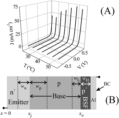 | ||
| Fig. 2 (A) Current (J) vs. voltage (V) curves for a single crystal Si solar cell, recorded using LSV at five degree intervals between 25 and 55 °C. (B) A schematic of a Si solar cell (not drawn to scale) including an n+-p diode, a p-p+ low-high BSF interface, and a back contact (BC) of Al and Si. | ||
Fig. 2B (not drawn to scale) schematically shows the internal arrangement of the test cell containing a BSF. The x axis indicates the coordinates of the n+-p and p-p+ BSF junctions at xj and x0, respectively. The widths of the diode SCR on the emitter and the base sides are wn and wp, respectively. The widths of the low (L) and high (H) sides of the p-p+ junction (hole-accumulation and hole-depletion layers, respectively) are wL and wH, respectively. The cell components considered in Fig. 2B will be referred to in the discussion of experimental data throughout this report.
For an illuminated solar cell with a BSF, the OCV (Voc) of the cell increases due to a contribution of the LH junction.16 For dark cells, however, Voc appears at 0 V, and does not serve as a useful indicator of the presence (or absence) of the BSF. Similarly, the D.C. J–V data of Fig. 2A do not contain any obvious signatures of the LH interface. As shown later in this report, these LH effects can be detected using IS measurements under strong FB.
3.2. A.C. Nyquist spectra and component-sensitive equivalent circuit of the solar cell
Fig. 3 displays illustrative Nyquist spectra for the Si solar cell, plotted as functions of D.C. FB voltages for three selected temperatures, (A) 25, (B) 40 and (C) 55 °C, where Z′ and Z′′ denote the real and imaginary components of the cell impedance, respectively. Explicatory Nyquist data (symbols), along with their CNLS fits (lines) are shown in Fig. 4A (for high FB) and B (for low/moderate FB) where T = 25 °C. The perturbation frequencies on each graph decrease in going from left to right. The analytical framework of IS developed in the field of traditional electrochemistry heavily utilizes the formalism of equivalent circuits to evaluate charge transport characteristics at interfaces.26 The same formalism is adapted in IS studies of non-electrochemical solar cells.8,9,12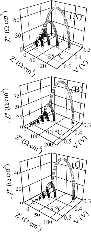 | ||
| Fig. 3 Typical Nyquist impedance spectra for an un-illuminated single crystal Si solar cell, recorded at different forward bias voltages under temperature control at (A) 25 (B) 40 and (C) 55 °C. | ||
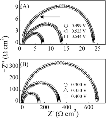 | ||
| Fig. 4 (A) Nyquist impedance spectra for the experimental solar cell, recorded without illumination at 25 °C, with (A) high or (B) low D.C. forward bias voltages. The arrow associated with the top-most graph in (A) points to the region where the characteristic impedance feature of the LH junction intersects with that of the n+-p diode. In (B) the impedance signature of the LH interface is overwhelmed by the substantially increased impedance of the n+-p diode at low FB voltages. | ||
The D.C. behaviors of the solar cells are commonly described in terms of single- or double-diode CEC models, and the A.C. response characteristics of these diodes are considered in the circuit models used for their IS studies.17 The CEC model used here to fit the experimental Nyquist spectra of Fig. 3 and 4 is shown in Fig. 5A. Here, Cj and Rj denote the capacitance and the resistance of the cell's n+-p diode, respectively. CLH and RLH are the corresponding elements of the low-high (LH) junction at the back surface of the cell; Rs is the net series resistance. Thus the main electrically relevant parts of the solar cell are clearly resolved in the detected circuit model, and this illustrates the component sensitive resolution of the CNLS analyzed IS results.
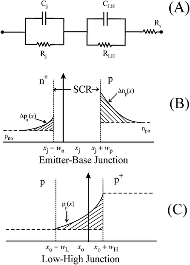 | ||
| Fig. 5 (A) Equivalent circuit model of the experimental solar cell, used here to obtain CNLS calculated fits to the experimental IS data. (B) A schematic diagram (not according to scale) of the n+-p diode junction showing the SCR (without displaying the immobile ion cores contained in it) and the voltage injected free carrier concentrations, Δnp and Δpn, in the quasi-neutral base (p) and emitter (n+) regions, respectively;19,27np0 and pn0 are the equilibrium minority carrier concentrations in the base and the emitter, respectively. (C) Schematically (not to scale) drawn concentration profile, pp(x), of holes in the p-p+ junction.28 The regions x0−wL ≤ x ≤ x0 and x0 ≤ x ≤ x0 + wH represent the hole-accumulation and hole-depletion regions, respectively. The value of pp increases from Na at x0−xL to Na+ at x0 + xH. | ||
The CLH-RLH loop only becomes detectable in the CEC at high FB voltages where the corresponding impedance of the Cj-Rj unit becomes smaller. This competitive effect of the n+-p diode and the LH interface can also be noted in the visibly different shapes of the Nyquist plots recorded at high-FB and low-FB voltages. The semicircular impedance arcs in Fig. 4B show the prevalence of the Cj-Rj unit at low-FB voltages. As the bias voltage is increased in Fig. 4A, these plots become gradually distorted due to the progressive development of a second impedance arc on the high-frequency (low impedance) side of the Nyquist data. This second component of the impedance spectra is the contribution of the CLH-RLH unit. The point marked by the arrow on the top graph of Fig. 4A indicates where the semicircles for the CLH-RLH and the Cj-Rj units intersect.
To examine the voltage and temperature sensitive trends of the experimental Nyquist plots, and also to discuss the CNLS results presented later in this report, it is useful to briefly note the expression of the spatially varying injected charge carriers in the quasi-neutral regions of the solar cell. For the n+-p junction considered, one has Nd > Na, where the donor and the acceptor oncentrations in the emitter and the base are, Nd and Na respectively. The FB injected electron density Δnp in the base (x>xj + wp) at a distance x from the front emitter surface has the form,19,27
 | (1) |
For n+-p junctions, wp ≫ wn, and the charge transport component of Δnp in the base dominates the impedance characteristics of the device. The total cell impedance experiences a drastic drop as the value of Δnp (and hence the cell's charge conduction) increases exponentially with V according to eqn (1). This is seen in Fig. 3 in the rapidly shrinking impedance arcs along the increasing directions of the voltage axes. The temperature dependencies of Z′ and Z′′ are controlled by that of Δnp in eqn (1); the diode ideality factor depends on T, and the product (m1T) in the first exponential term plays an important role, as the value of m1 depends on T.17,25
The spatial concentration profile of holes, pp(x) at the LH (p-p+) junction is schematically shown in Fig. 5C, and has the form28
| pp(x) = Na+exp[− {Vp0 − VLH + ψ(x)}(VT)−1], | (2) |
Under FB of the solar cell, both the diode and the LH junctions are forward biased and the applied voltage acts to compress the space charge layers at both these junctions.28 However, the LH junction (< 1 μm) as well as the full BSF region (∼10–15 μm) is considerably thin compared to the base length (∼300 μm).29 Consequently, at moderate FB voltages, the net impedance of the LH junction is mostly engulfed by the comparatively much larger impedance of the diode junction.8 It is due to this reason that the CLH−RLH loop of the CEC is not detected in IS until a strong FB is applied to sufficiently lower the competing impedance of the Cj−Rj sector.
The component sensitive attributes of the observed CEC represent the main added features of CNLS supported IS analysis with respect to the traditional capacitance studies of p-n junctions.13,30,31 The capacitance techniques, often based on small signal perturbations like IS, frequently use voltage (as well as frequency) selective signatures of the SCR and diffusion capacitances to separately identify these elements. The same approach is also used in IS measurements to resolve the contributions of these two types of capacitances from the recorded net device capacitance. However, simple considerations of capacitance measurements that often assume just a combination of Rj and Cj, do not form the full analytical framework necessary for quantitative characterization of multi-component systems such solar cells. On the other hand, the component specific CEC models available from CNLS analyzed IS data can detect and describe the detailed features of various additional elements such as Rs, CLH and RLH that are coupled with the n+-p diode in the solar cell. This observation is illustrated further in the following Sections.
3.3. Series resistance
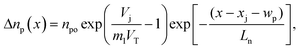
Voltage and temperature dependent values of Rs are shown in Fig. 6A, where the symbols represent data points obtained from CNLS analyses of experimental Nyquist plots. On the x-axis of this panel, the measured Rs values are combined with J (simult aneously recorded with the IS data) to convert the voltage scale of V to that of Vj. The Rs plot at each temperature goes through a maximum with increasing FB. This non-ohmic voltage sensitive feature of Rs for Si solar cells has been observed previously.8,32 To extract the maximum values of Rs from the given set of data points, the experimental graphs in Fig. 6A were subjected to polynomial interpolation by following the approach commonly used in the fields of shape analysis and computational geometry.33 The solid lines in Fig. 6A show plots of these (sixth order) interpolating polynomial fits to the data. The Rs-maxima were determined from the local differentials of the fits. Graph (a) in Fig. 6B shows the temperature sensitive values of the voltage Vjp, where the maxima in the Rs plots were determined from this procedure.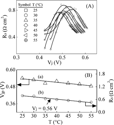 | ||
| Fig. 6 (A) Temperature (T) dependent values of the series resistances (Rs) of the Si solar cell, plotted against the diode junction potential Vj. The symbols denote data points, obtained by CNLS fitting experimental impedance spectra at different temperatures. The solid lines represent interpolating polynomial fits to the data, used to determine the peaks in the plots by calculating local differentials. (B) Graph (a) linked to left ordinate axis shows the voltages (Vjp) corresponding to the peaks in Rs, taken from panel (A) and plotted against T. The symbols are data points and the linear fit to these has a slope of −1.64 × 10⁻³ V °C−1 with an ordinate intercept of 0.58 V. Graph (b) using the right ordinate axis shows temperature dependent values of Rs at Vj = 0.56 V. The symbols are data points taken from panel (A). The linear fit to these points on (b) has a slope and an ordinate intercept of −7.11 × 10 −3Ω cm2°C−1 and 1.05 Ω cm2, respectively. | ||
To account for the observed non-ohmic behavior of Rs, the net series resistance of the solar cell can be written as Rs = (Rs0 + Rbc), where Rs0 is the total ohmic contribution of all the contact resistances that only responds to variations in the cell temperature but not the voltage; the non-ohmic part Rbc of the back contact responds to both. According to previously reported observations, the non-ohmic part of Rs arises from tunneling currents at the low-barrier Schottky diode formed by the p-Si/Al interface on the back surface of the solar cell.34,35 As the voltage at this interface changes in response to variations in the value of Vj, the tunneling resistance Rbc changes accordingly. The potential induced maximum of Rbc, which occurs at the Fermi degeneracy of the semiconductor, has been attributed previously to the observed voltage induced peak of Rs.8,35 This mechanism is consistent with the downward trend of Vjp with increasing temperatures observed in Fig. 2B.36
Previously reported experiments have shown that at low FB (V < 0.4 V) and moderate RB potentials, Rs is voltage independent and entirely ohmic (Rs ≈ Rs0).8,18 It has also been demonstrated previously that, this ohmic Rs0 increases linearly with increasing temperatures in the 25–55 °C range, which is consistent with the metal-dominated behavior the cell's contact resistances.17,25 Other authors have also reported similar temperature induced increases in the ohmic series resistances of Si solar cells.36,37 However, in its peak region, and especially at voltages above Vjp, Rs in Fig. 6A tends to decrease with increasing temperatures. This is prominently shown in Fig. 6B using the illustrative plot (b) of Rsvs. T, taken at Vj = 0.56 V. This temperature dependence of Rs is opposite of that expected in terms of a pure ohmic makeup of the series resistance, but is consistent with the description of the tunneling resistance proposed above.8,35–38 Based on these observations, it is expected that at high FB voltages Rs is dominated by its non-ohmic part Rbc.
Over the temperature range sampled in Fig. 6B, the plotted Rs data appear mostly linear. However, these data, taken at a fixed Vj, also contain the rather complex temperature receptive correlation between Vj and the potential drop at the Al-Si interface; it is the latter voltage that directly governs the non-ohmic component of Rs. Therefore, the apparently linear Rsvs. T graph observed here may be more general over wider ranges of temperature and voltage.
3.4. Diffusion controlled capacitance, resistance and minority carrier lifetime
Fig. 7 shows the diode supported (A) capacitance and (B) resistance of the solar cell studied in this work. Both the temperature and the voltage dependent variations of these parameters are examined in this Figure. The voltage ranges explored at the different sampling temperatures represent the regions surrounding the peaks in Rs shown in Fig. 6A. The symbols in Fig. 7 denote data points and the lines show the general trends of the data. The voltage scales are normalized to Vj using measured values of J(V) and Rs(V). | ||
| Fig. 7 (A) Capacitance, Cj, and (B) resistance, Rj, of the n+-p diode junction of the Si solar cell, plotted as functions of temperature and forward bias junction voltages. The data sets are taken at 5 degree intervals between 25 and 55 °C. The lines connecting the data points (symbols) show the linear trends of the semi-log plots. | ||
To examine the results for the A.C. parameters in Fig. 7, we note that the CEC (Fig. 5A) representing these parameters is just an A.C. version of the D.C. two-diode model commonly used to describe electrical properties of Si solar cells. The two separate diodes considered in such a model represent charge recombination processes occurring in the quasi-neutral base (diode 1) and the ionized SCR (diode 2).25,39 In the A.C. description of the two-diode model Cj contains the capacitive contributions of both diodes and the SCR; Rj contains the resistances of both diodes as well as the shunt resistance Rsh.12 Thus, Cj = (Cd1 + Cd2 + CT), and (Rj)−1 = [(Rd1)−1 + (Rd2) + (Rsh)−1], where CT is the transition capacitance (inversely proportional to the value of (xn + wp) of the diode SCR. However, as shown previously, Rsh and CT have negligible contributions to the measured impedances in the FB voltage range explored here.7,8,12 Therefore, under the experimental conditions of the present work, Cj ≈ (Cd1 + Cd2), and Rj ≈ (Rd1Rd2)/(Rd1 + Rd2).
The charge-recombination mechanism that gives rise to the (Rd1−Cd1) impedance elements (diode 1 mentioned above) originates from the diffusion of charge carriers in the quasi-neutral regions of the solar cell. This process is only activated to a measurable extent under high FB conditions, where the SCR recombination effects responsible for the (Rd2−Cd2) elements are practically absent.8,19 On the other hand, the impedance elements of charge recombination in the SCR (diode 2) dominate the low and moderate FB voltages, where the effects of diode 1 become negligible.
The capacitance of diode 1 is defined as Cdl = (dQ/dVj), where Q is the total charge of diffused minority carriers as indicated by the shaded areas in Fig. 5B. For the n+-p cell used here (wn≪wp), this Q can be obtained by integrating eqn (1) between the limits, x = xj + wp, and x = ∞. These calculations yield the result,8,19,27
 | (3) |
Recombination of charge carriers in the SCR, as represented by the second diode of the two-diode model is confined within a limited region around the n+-p junction.24Cd2 and Rd2 are associated with the recombination impedance of this specific region, and can be expressed in a form similar to eqn (3). An approximate expression of Cd2 can be written as: Cd2=C0d2exp[Vj/(m2VT)] = (τ2/2Rd2), where C0d2 = (ew0ni)/(4m2VT),17,18,25 and it is assumed that [w0/(m2VT)] ≫ (dw0/dVj) at the voltage where SCR recombination is active. Here m2 is the ideality factor of the diode representing charge annihilation in the SCR; w0 is a characteristic length over which the rate of recombination drops on both sides of xj in the SCR. τ2is the carrier lifetime associated with SCR-localized recombination, and can be different from τ1, as the two parameters originate from separate mechanisms.19,25
At each sampling temperature, Cj exhibits its exponential voltage dependence according to the mutually similar analytical forms of Cd1 and Cd2.19 This leads to the nearly linear semi-log graphs in Fig. 7A. These capacitance graphs also indicate a change of slope in the low FB region, because the location of the predominant charge recombination process switches from the quasi-free base to the SCR as the FB voltages are lowered. Since the mechanisms of these two recombination types are different, their associated diode ideality factors m1 and m2 also have different values. Typically, m1 ≈ 1 and m2 ≈ 2, and these different diode factors lead to the different slopes of the Cj-Vj semi-log plots in Fig. 7.13,19,25 The slopes of these graphs are inversely proportional to the respective diode ideality factors, and thus, are smaller in the low FB region (where m2 dominates), and higher in the high FB region (where m1 dominates). These slopes are also inversely proportional to T (through VT), and their voltage dependent variations in response to the different values of m1 and m2 are most noticeable for the graphs observed at the lower temperatures.
The net resistance of the n+-p diode under moderate-high FB has the form:17
| Rj ≈ [2Cd1(τ1)−1 + 2Cd2(τ2)−1]−1, | (4) |
To examine the combined temperature and voltage dependencies of the minority carrier lifetimes, an effective carrier lifetime parameter τj can be defined as follows:
 | (5) |
Fig. 8 shows the voltage and temperature sensitive values of τj, obtained from the Rj and Cj data of Fig. 7. The shapes of the τj−Vj graphs are different for the high and low FB regions, because base recombination dominates (τj ≈ τ1) at high FB, and SCR recombination dominates (τj ≈ τ2) at low FB. At the higher FB potentials, τj increases with increasing Vj by largely following the voltage dependence of Cj. This effect has also been reported by Suresh,12 and it arises from injection dependent variations of carrier lifetimes. If recombination centers (localized trap states capturing carriers of both polarities) control charge transport in the quasi-neutral base, the effective carrier lifetime is determined by the relative rates of capture and re-emission of the two types of particles. FB-induced charge injection affects these rates to alter the steady state probability of trap occupation, and acts in turn to change the values of τ1.15,19
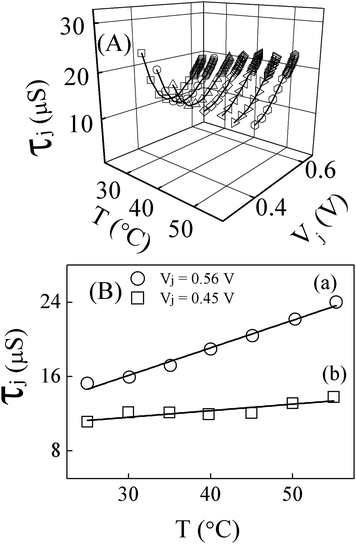 | ||
| Fig. 8 (A) Temperature and forward bias dependent effective lifetime τj of minority carriers within the n+-p diode region of the solar cell. The lines through the data points (symbols) show the general trend of the data. (B) Values of τj, recorded at different temperatures with Vj set at two forward biased voltages, (a) 0.56 V and (b) 0.45 V. The linear fits to the data have the slopes, (a) 0.297 and (b) 0.070 μs °C−1. The corresponding ordinate intercepts are (a) 7.2 and (b) 9.5 μs. | ||
With decreasing FB voltages, τj in Fig. 8A decreases and eventually tends to rise again with further lowering of potentials. These effects, which are most noticeable at the lower temperatures have been studied previously under room temperature conditions.8,9 A partial contribution to the observed trend of τj at Vj < 0.35 V could come from the gradually increasing incorporation of Rsh in the value of Rj measured at low bias voltages. Such a contribution of Rsh, however, should remain relatively weak until the solar cell is reverse-biased.8,12 On the other hand, as discussed below, an assessable component of the voltage dependence of τj between 0.3 and 0.5 V could be rooted in a competitive interplay between the two types of recombination mechanisms associated with τ1 and τ2.
In the mid-FB region both the base- and the SCR-recombination mechanisms operate, and hence the net recombination process is most efficient in this region.19 Owing to this efficient annihilation of charge carriers, the effective carrier lifetime is the smallest in this voltage region. Such an effect could be associated with the “valley” observed in the mid-section of a number of the nearly U-shaped τj−Vj plots in Fig. 8A (at the higher temperatures the full shapes of these plots are not visible within the voltage limits explored). With voltages dropping further below the mid-FB range, the base recombination essentially shuts down, so the lifetime increases again. Bruno et al. have measured room-temperature carrier lifetimes as a function of FB voltages for a BSF-Si solar cell.40 These authors' data are similar to the τj−Vj graphs shown here, especially to those collected at the lower temperatures in Fig. 8A. Bruno et al. have explained their data using numerical calculations of combined SCR and base recombination steps as mentioned above in the context of eqn (5). Moreover, based on these authors' results, the prominence of the U-shaped feature of the τj−Vj graphs should depend on the presence/strength of surface recombination that interferes with the bulk effects.
In view of the above considerations, it is most likely that the general trends of the plots shown in Fig. 8A are affected by both bulk (SCR as well as base) and back-surface recombination effects. If surface recombination is present, its contribution to the measured carrier lifetime cannot be easily separated from that of bulk recombination unless additional procedures are incorporated.41 As noted above τj should have its minimum values at the intermediate FB voltages where the base and SCR recombination processes are simultaneously present. In addition, this already increased charge annihilation effect would be enhanced further in the presence of surface recombination.40 For thin solar cells (wb ≪ Ln) like the one used here, this type of coupling between surface and bulk recombination steps is expected, and suggestive evidence for this effect in the presently used system is discussed later in Section 3.7 of this report. Furthermore, unlike the quasi-free base, the SCR is equipped with an electric field, the effects of which increase with decreasing FB as the diode SCR progressively widens under these conditions.19,25 As shown by Canali et al.,42 such a field could lower the effective diffusion coefficient of charge carriers in the active region of the field, and this in turn could contribute to raising the values of τ2 with decreasing FB potentials.
At fixed voltages, τj exhibits a general increasing trend with increasing temperatures. Sample plots illustrating this effect for two selected FB voltages are shown in Fig. 8B. Previous authors have reported similar linear τjvs. T graphs for Si solar cells operated in the temperature range used here,43 and Ichimura et al. have explained the mechanism for this effect using the Shockley-Read-Hall (SRH) recombination theory.44 Earlier results of such temperature dependent carrier lifetimes have been linked to thermally induced changes in the carrier capture cross sections of trap centers.45 The recombination mechanisms probed here are voltage-dependent, and the trap states associated with the two mechanisms also are likely to be different at the different voltages. Due to this reason, and as seen in Fig. 8B, the slopes of the τjvs. T graphs depend on the cell voltage.
3.5. Electrical parameters of the back surface field
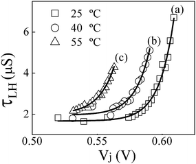
The interpretation used here for the RLH and CLH parameters, namely their association with the solar cell's BSF region was set forth in a previous study.8 This attribution was based primarily on a comparison of the D.C. voltage drop (VLH) measured across the RLH element of the test cell with respect to the built-in voltage (Vp0) of the p-p+ interface. Theory predicts that the bias voltage at the p-p+ junction must be noticeably smaller than Vp0, and hence VLH should have this feature if it represents the LH junction voltage as proposed here.16,29 For Na ≈ 1016 cm−3 and Na + ≈ 1019 cm−3 (typical values) one has Vp0 = VTln(Na+/Na) ≈ 7VT where VT = 26 mV at room temperature.28 In comparison with this Vp0, the experimental values of VLH have been found only to vary between 5 and 15 mV by changing Vj between 0.45 and 0.60 V at 25 °C.8 This experimentally established inequality, VLH<Vp0, has served as a key factor to locating the origin of the RLH-CLH unit at the p-p+ junction of the solar cell.8,28The IS-measured values of (A) RLH and (B) CLH are plotted in Fig. 9 as functions of temperature and FB voltages. Fig. 10A shows Vj and T dependent graphs of the characteristic time constant (τLH) of charge transport associated with these elements. Here, τLH = 2CLHRLH, with the factor of 2 introduced phenomenologically in analogy with the corresponding definition of τj. If the electrons injected in the base enter in the LH region, the lifetime of such electrons would typically have values that are at least an order of magnitude less than those of τLH observed in Fig. 10A.28 Therefore, this τLH cannot be attributed to electron recombination in the LH junction. Likewise, the minority carrier lifetime in the n+ emitter should also be about an order magnitude smaller than the measured values of τLH.16 These comparisons lead to the proposed characterization of τLH as the relaxation time of holes in the BSF region.
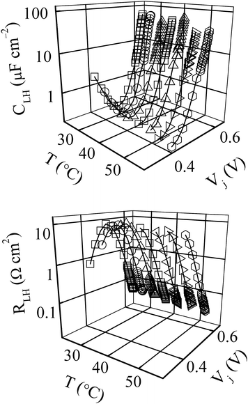 | ||
| Fig. 9 (A) Temperature and forward bias dependent capacitance, CLH, and (B) resistance RLH of the low-high junction of the BSF solar cell studied in this work. The lines through the data points (symbols) show the general inclinations of the data. | ||
![(A) Relaxation time, τLH, of hole-carriers at the p-p+ low-high junction of the experimental Si solar cell, determined in the absence of illumination as functions of T and forward biased Vj using the results from Fig. 9. The symbols denote experimental data and the lines indicate the general trends of the data. (B) Functional form of the temperature dependence of τLH, examined at a high FB voltage, 0.56 V. The symbols are data points taken from panel (A), and the line denotes an empirical fit to the data, expressed as: τLH=τ0LH + a[exp(bT)], with τ0LH = 1.745 μs, a = 0.012 μs, and b = 0.097 °C−1.](/image/article/2012/AY/c1ay05455d/c1ay05455d-f10.gif) | ||
| Fig. 10 (A) Relaxation time, τLH, of hole-carriers at the p-p+ low-high junction of the experimental Si solar cell, determined in the absence of illumination as functions of T and forward biased Vj using the results from Fig. 9. The symbols denote experimental data and the lines indicate the general trends of the data. (B) Functional form of the temperature dependence of τLH, examined at a high FB voltage, 0.56 V. The symbols are data points taken from panel (A), and the line denotes an empirical fit to the data, expressed as: τLH=τ0LH + a[exp(bT)], with τ0LH = 1.745 μs, a = 0.012 μs, and b = 0.097 °C−1. | ||
The above proposal regarding the origin of τLH can be enumerated further by comparing the temperature dependence of τLH at a fixed FB voltage with the corresponding behavior of τj at the same voltage. Fig. 10B shows such a typical graph of τLH against T for Vj = 0.56 V. This graph deviates noticeably from the characteristic linear behavior of τj seen over the same temperature range at the same FB voltage in plot (a) of Fig. 8B. The τLH graph in Fig. 10B, as well as similar ones recorded at its neighboring FB voltages could be characterized as exponential variants with respect to T. The solid line in Fig. 10B indicates this trend. The largely decoupled temperature dependencies of τLH and τj also suggest that these two parameters originate from different mechanisms. This observation provides additional basis for not correlating the LH parameters directly with electron recombination in the base.
For Al-BSF Si solar cells like the one used in this work, the BSF region is a 10–15 μm thick layer, sandwiched between the p-Si base and the Al back contact.46,47 However, the potential gradient supporting the BSF is confined mostly within a narrower region of the LH interface. The voltage drop VLH across this interface also determines the values of the LH impedance elements. As shown previously,8CLH = (∂QLH/∂VLH), and RLH ≈ (∂J/∂VLH) for a dark cell under FB. Here, QLH = |e| pLHp, and pLHp denotes the total hole concentration in the p-p+ region (shaded area in Fig. 5C). The latter quantity can be obtained through numerical integration of pp(x) from eqn (2) over the full (voltage dependent) width of the LH interface. Thus, both elements of the LH junction, and hence their composite term τLH should vary with VLH by following the typical voltage dependence of free charge carrier injection as characterized by eqn (2).
Due to the inclusion of multiple interdependent variables in the above expressions of CLH and RLH, analytical forms of these latter parameters are not readily calculable.28,48 Furthermore, since VLH changes in a rather non-trivial way with variations in Vj, it is difficult to establish a direct correlation between Vj and the corresponding variations observed in the values of CLH and RLH. Nevertheless, in the high FB region, VLH has been shown to vary almost linearly with Vj.8 Based on this observation, it is possible that under strong FB, the voltage dependence of τLH becomes predominantly exponential, similar to that of τj. Fig. 11 shows such values of τLH recorded as functions of Vj at high FB for three different temperatures. The empirical fits (lines) to the data points (symbols) have the following general form: τLH = A + A'exp[(Vj−C)/D]. Here, A = (a) 1.669, (b) 1.960 and (c) 1.997 μs; A'= (a) 1.365, (b) 20.638 and (c) 106.46 ns; C = (a) 0.516, (b) 0.532 and (c) 0.525 V; D = (a) 0.0114, (b) 0.0116 and (c) 0.0123 V. Thus, consistent with the considerations of free charge carrier diffusion, all three plots in Fig. 11 fit satisfactorily to the exponential form of Vj.
 | ||
| Fig. 11 Voltage dependence of τLH, examined under high FB at three different temperatures. The symbols are data points taken from Fig. 10A, and the lines are empirical fits to the data. | ||
While the results of Fig. 10 and 11 are consistent with the proposed description of the LH elements, one cannot rule out the possibility that electron diffusion in the immediate front of the BSF also plays a role in the development of these impedance elements. Experimental results that provide the background for considering this possibility can be noted in recent publications, according to which, minority carrier lifetime may locally vary depending on the distance from the back surface.49,50 Without the BSF, surface recombination would lower the bulk electron lifetime in the surface region. The BSF repels electrons back into the base to reduce this process, and the end region of the base affected by these BSF-driven electrons may exhibit a measurably different electrical response in IS. In that case, electron recombination in the base region adjacent to the BSF could also serve as an originating factor for the detected LH elements. Further studies will be necessary to address this topic in detail.
Regardless of these mechanistic details, from phenomenological considerations, CLH and RLH should be inversely and directly proportional to the thickness of the LH space charge layer, respectively. Because this layer plays a critical role in dictating the extent of surface recombination, and because τLH largely follows the voltage dependence of CLH (according to Fig. 9A and 10A) a drop in the value of τLH should indicate a thinning of the LH layer. Thus, the voltage sensitive values of τLH can be used as a measure of the strength of the BSF, and hence as a probe of surface recombination effects on the diode parameters.
3.6. Comparison of measured junction parameters with previously reported results for device specific configurations
The structural and compositional details of n+-p diodes, as well as those of p-p+ LH junctions widely vary depending on their device-specific applications.51–55 Moreover, the electrical characteristics of these individual junctions can change when incorporated together in a single device like a solar cell. In addition, the current collecting contacts of a solar cell introduce the unavoidable series resistance that affects the measurement of the cell's junction parameters; these additional Rs effects often are absent or minor, when simple n+-p or p-p+ subunit devices are characterized in the same approach. Due to these multiple reasons, it is difficult to quantitatively compare the IS-measured parameters for the solar cell with those of separately fabricated n+-p and p-p+ junctions. Nevertheless, an overall assessment can be made in this regard, focusing specifically on the charge relaxation times, to check how these parameters vary between the combined (n+-p-p+) and the uncombined (n+-p and p-p+) configurations. Such comparisons typically are limited to device structures based on mutually similar fabrication methods as well as similar carrier concentrations; some illustrative examples of these cases are briefly noted below.Previous A.C. measurements using a commercial n-p diode have yielded minority carrier lifetimes in the 2–6 μs range.56 Likewise, minority carrier (electron) lifetimes for relatively large n+-p diodes have been obtained from J–V measurements at room temperature, and the reported results (corrected for perimeter effects) for low oxygen-content samples have varied between 25 and 30 μs.57 Despite their different applications, these diodes are found to support carrier lifetimes that are of the same order of magnitude of τj presented here in Fig. 7. This indicates how the diode junction dominates the overall charge recombination characteristics of the solar cell.
In comparison with the cases of n-p and n+-p diodes, experimental results for Si based p-p+ junctions (especially those relevant for solar cells) are scarce in the commonly available literature. However, the work reported by Lago-Aurrekoetxea et al. can be noted in this context, where a value of 5 μs has been found for the relaxation time of holes within a 10.8 μm thick Al-diffused region of a p-type Si wafer.58 This value is comparable to those plotted here in Fig. 10A and 11. The observed agreement between the two sets of results is expected, because the device configuration considered in Ref. 58 was specifically designed for BSF solar cells.
While the individually measured diode and LH parameters fit reasonably well within the basic framework of the IS results for a solar cell, only the latter results indicate how the different cell components interact. As we discuss next, these interactions are responsible for various mutually coupled voltage and temperature dependent features of the combined component parameters that remain absent from the corresponding parameters measured for the separate components.
3.7. Interplaying roles of Rs, τj and τLH
The above discussion, in combination with previously published results for VHL,8 provides a framework for tying together the observed behaviors of Rs, τj and τLH. According to Fig. 2A, the onset of sizable diode currents occurs at a threshold FB voltage where the current exhibits its “knee” like feature. As shown in ref. 8, the values of VLH go through a relatively broad maximum around this voltage. The diode voltage where VLH begins to increase corresponds approximately to the onset in the peak of Rs. This suggests that the potential drop at the Si-Al rear contact (which is responsible for the voltage dependence of Rs) of the cell varies in a coupled mode with the variation of VLH as the values of Vj are changed. This is plausible because the p+ side of the BSF represents essentially the same region as the semiconductor side of the Si–Al contact. This close proximity of the back contact to the BSF layer can force the variations of the non-ohmic part of Rs to be strongly affected by variations in VLH.As noted in the discussions of Fig. 5C and 8A, the minority carrier density profile occupies the back surface region due to the condition, wb ≪ Ln. Therefore, the electrons in the base are prone to surface recombination at the Si-Al interface. This surface recombination should be the strongest at the peak region of VLH, where the LH space charge layer is most efficiently compressed and therefore, is least effective in repelling electrons.29 Hence, τLH drops down to its minimum value in this voltage region, and at the same time, interference of surface recombination enhances the observed dips in the τj−Vj plots. Thus the minimum values of τj and τLH occur essentially in the same (moderate FB) voltage region where VLH, the effective FB of the LH junction attains its maximum value. On both sides of this voltage region, VLH drops again to lower values,8 and allows the p-p+ space charge layer to re-expand, which in turn returns τLH to its higher values. Then the uncompressed LH layer can once again shield the charge dynamics of the base region from interfering effects of surface recombination. This corresponds to the rising trend of τj at low FB voltages.
4. Conclusions
The experiments reported in this work explore the electro-analytical capabilities of IS and LSV for combined temperature and voltage dependent studies of non-electrochemical solid state photovoltaic systems. A specific advantage of this characterization approach is that, at a set D.C. voltage under temperature control, the different parameters of a test cell can be concurrently measured with a single IS scan. This allows for adequately comparing different D.C. and A.C. parameters under the same set of externally controlled conditions.The series resistance of the solar cell contains a non-ohmic component with a voltage dependence that is consistent with the signature of a Schottky junction. The measured minority carrier lifetimes indicate the presence of two types of recombination mechanisms that originate in the quasi-neutral base and the SCR under strong and moderate FB voltages, respectively. Consistent with previously reported results, these lifetimes increase with increasing bias voltages12,39 and increasing cell temperatures44,45 within the ranges of these variables explored here. The IS results also show how voltage and temperature variations affect the charge dynamics of the BSF junction in the solar cell. In addition, suggestive evidence is found for a possible coupling between the parameters of the base and the BSF.
The solar cell parameters characterized here with the collective set of IS and LSV results are largely affected by the material/device processing conditions used for device fabrication. This underscores the utility of electro-analytical tests in aiding the development/processing of new cost-effective Si based solar cell materials (such as ultra-metallurgical grade Si59,60). The temperature and voltage dependencies of cell parameters based on such trial materials can be quantitatively characterized using LSV and IS, and subsequently, can be correlated with material designs and processing conditions as a useful tool for optimizing the control variables of the latter.
Acknowledgements
This work was supported by the Army Research Office (Grant No. W911NF-05-1-0339).References
- Electroanalytical Methods: Guide to Experiments and Applications, ed. F. Scholz, Springer, Heidelberg, 2nd edn, 2010 Search PubMed.
- F. Fabregat-Santiago, J. Bisquert, E. Palomares, L. Otero, D. Kuang, S. M. Zakeeruddin and M. Grätzel, J. Phys. Chem. C, 2007, 111, 6550–6560 CAS.
- Nanostructured and Photoelectrochemical Systems for Solar Photon Conversion, ed. M. D. Archer and A. J. Nozik, Imperial College Press, London, 2008, Vol. 3 Search PubMed.
- Y. Y. Proskuryakov, K. Durose, M. K. Al Turkestani, I. Mora-Seró, G. Garcia-Belmonte, F. Fabregat-Santiago, J. Bisquert, V. Barrioz, D. Lamb, S. J. C. Irvine and E. W. Jones, J. Appl. Phys., 2009, 106, 044507-1–9 CrossRef.
- L. Raniero, E. Fortunato, I. Ferreira and R. Martins, J. Non-Cryst. Solids, 2006, 352, 1880–1883 CrossRef CAS.
- R. Anil Kumar, M. S. Suresh and J. Nagaraju, Sol. Energy, 2004, 76, 417–421 CrossRef.
- Mora-Seró, G. Garcia-Belmonte, P. P. Boix, M. A. Vázquez and J. Bisquert, Energy Environ. Sci., 2009, 2, 678–686 Search PubMed.
- J. E. Garland, D. J. Crain, J. P. Zheng, C. M. Sulyma and D. Roy, Energy Environ. Sci., 2011, 4, 485–498 CAS.
- I. Mora-Seró, Y. Luoa, G. Garcia-Belmonte, J. Bisquert, D. Muñoz, C. Voz, J. Puigdollers and R. Alcubill, Sol. Energy Mater. Sol. Cells, 2008, 92, 505–509 CrossRef.
- S. Kumar, P. K. Singh and G. S. Chilana, Sol. Energy Mater. Sol. Cells, 2009, 93, 1881–1884 CrossRef CAS.
- H. Anantha Krishna, N. K. Misra and M. S. Suresh, J. Instr. Soc. of India, 2009, 39, 53–56 Search PubMed.
- M. S. Suresh, Sol. Energy Mater. Sol. Cells, 1996, 43, 21–28 CrossRef CAS.
- S. M. Sze and K. K. Ng, Physics of Semiconductor Devices, Wiley, Hoboken, 2007 Search PubMed.
- A. Neugroschel, IEEE Trans. Electron Devices, 1981, 28, 108–115 CrossRef.
- J. Nelson, The Physics of Solar Cells, Imperial College Press, London, 2004 Search PubMed.
- H. J. Hovel, in: R. K. Willardson and A. C. Beer, ed. Semiconductors and Semimetalsvol. 11, Academic Press, New York, 1975 Search PubMed.
- J. E. Garland, D. J. Crain and D. Roy, Sol. Energy, 2011 DOI:10.1016/j.solener.2011.08.029.
- J. E. Garland, Ph.D. Thesis, Clarkson University, 2011.
- S. S. Li, Semiconductor Physical Electronics, Plenum Press, New York, 1993 Search PubMed.
- J. E. Garland, C. M. Pettit and D. Roy, Electrochim. Acta, 2004, 49, 2623–2635 CrossRef CAS.
- B. A. Boukamp, Solid State Ionics, 1986, 20, 31–44 CrossRef CAS.
- M. Wolf and H. Rauschenbach, Adv. Energy Convers., 1963, 3, 455–479 CrossRef.
- E. Radziemska, Energy Convers. Manage., 2005, 46, 1485–1494 CrossRef CAS.
- C. T. Sah, Fundamentals of Solid State Electronics, World Scientific, Singapore, 1991 Search PubMed.
- A. Goetzberger, J. Knobloch and B. Voss, Crystalline Silicon Solar Cells, J. Wiley, New York, 1998 Search PubMed.
- E. Barsoukov and J. R. Macdonald, ed. Impedance Spectroscopy, Wiley, Hoboken, 2nd edn, 2005 Search PubMed.
- B. G. Streetman, Solid State Electronic Devices, Prentice Hall, Englewood Cliffs, 1995 Search PubMed.
- S. N. Singh and P. K. Singh, IEEE Trans. Electron Devices, 1991, 38, 337–343 CrossRef.
- O. von Roos, J. Appl. Phys., 1978, 49, 3503–3510 CrossRef CAS.
- B. R. Chawla and H. K. Gummel, IEEE Trans. Electron Devices, 1971, 1(8), 178–195 CrossRef.
- M. Ohtomo, IEEE Trans. Microwave Theory Tech., 1974, 22, 709–718 CrossRef CAS.
- O. Tuzun, S. Oktik, S. Altindal and T. S. Mammadov, Thin Solid Films, 2006, 511–512, 258–264 CrossRef CAS.
- F. Cazals and M. Pouget, Comp. Aided Geom. Design, 2005, 22, 121–146 CrossRef.
- D. Schroeder, in: W. Fichtner and D. Aemmer ed., Simulation of Semiconductor Devices and Processes, Vol. 4, Hartung-Gore Verlag, Zurich, 1991, p. 313-319 Search PubMed.
- J. W. Conley, C. B. Duke, G. D. Mahan and J. J. Tiemann, Phys. Rev., 1996, 150, 466–469 Search PubMed.
- Ö. Faruk Yüksel, Phys. B, 2009, 404, 1993–1997 CrossRef.
- E. Radziemska, Int. J. Energy Res., 2006, 30, 127–134 CrossRef.
- S. K. Sharmat, K. B. Samuel, N. Srinivasamurthy and B. L. Agrawal, J. Phys. D: Appl. Phys., 1990, 23, 1256–1260 CrossRef.
- M. A. Green, Progr. Photovolt.: Res. Appl., 2003, 11, 333–340 CrossRef CAS.
- C. J. Bruno, M. G. Martínez Bogado, J. C. Plá and J. C. Durán, Phys. Status Solidi A, 1999, 174, 231–238 CrossRef CAS.
- J. A. Giesecke, M. Kasemann, M. C. Schubert, P. Würfel and W. Warta, Progr. Photovolt.: Res. Appl., 2010, 18, 10–19 CrossRef CAS.
- C. Canali, C. Jacoboni, G. Ottaviani and A. Alberigi-Quaranta, Appl. Phys. Lett., 1975, 27, 278–280 CrossRef CAS.
- R. A. Kumar, M. S. Suresh and J. Nagaraju, Sol. Energy Mater. Sol. Cells, 2005, 85, 397–406 CrossRef CAS.
- M. Ichimura, H. Tajiri, T. Ito and E. Ara, J. Electrochem. Soc., 1998, 145, 3265–3271 CrossRef CAS.
- D. J. Sandiford, J. Appl. Phys., 1959, 30, 1981–1986 CrossRef CAS.
- V. Meemongkolkiat, K. Nakayashiki, D. S. Kim, R. Kopecek and A. Rohatgia, J. Electrochem. Soc., 2006, 153, G53–G58 CrossRef CAS.
- H. C. Fang, C. C. Chang, C. P. Liu, H. S. Chung and C. L. Huang, J. Electrochem. Soc., 2010, 157, H246–H249 CrossRef CAS.
- S. S. De, A. K. Ghosh, M. Bera, A. Hajra and J. C. Haldar, Phys. B, 1996, 228, 363–368 CrossRef CAS.
- A. K. Sharma, S. N. Singh, N. S. Bisht, H. C. Kandpal and Z. H. Khan, Sol. Energy Mater. Sol. Cells, 2011 DOI:10.1016/j.solmat.2011.04.027.
- P. Drummond, A. Kshirsagar and J. Ruzyllo, Solid-State Electron., 2011, 55, 29–36 CrossRef CAS.
- G. Garcia-Belmonte, J. Bisquert and V. Caselles, Solid-State Electron., 1998, 42, 939–941 CrossRef CAS.
- F. A. Lindholm, A. Neugroschel, C.-T. Sah, M. P. Godlewski and H. W. Brandhorst, Jr, IEEE Trans. Electron Devices, 1977, ED-24, 402–410 CrossRef.
- J. A. del Alamo and R. M. Swanson, IEEE Trans. Electron Devices, 1987, ED-34, 1580–1589 CrossRef CAS.
- S. Y. Lee and D. K. Schroder, Solid-State Electron., 1999, 43, 103–111 CrossRef CAS.
- H. Väinölä, J. Storgårds, M. Yli-Koski and J. Sinkkonen, Mater. Sci. Eng., B, 2002, B91–92, 421–424 Search PubMed.
- M. L. Lucia, J. L. Hernandez-Rojas, C. Leon and I. Mártil, Eur. J. Phys., 1993, 14, 86–89 CrossRef.
- J. Vanhellemont, E. Simoen and C. Claeys, Appl. Phys. Lett., 1995, 66, 2894–2896 CrossRef CAS.
- R. Lago-Aurrekoetxea, C. del Cañizo, I. Tobías and A. Luque, Solid-State Electron., 2005, 49, 49–55 CrossRef CAS.
- J. Degoulange, I. Périchaud, C. Trassy and S. Martinuzzi, Sol. Energy Mater. Sol. Cells, 2008, 92, 1269–1273 CrossRef CAS.
- G. delCoso, C. delCañizo and W. C. Sinke, Sol. Energy Mater. Sol. Cells, 2010, 94, 345–349 CrossRef CAS.
Footnote |
| † This article is part of a web theme in Analyst and Analytical Methods on Future Electroanalytical Developments, highlighting important developments and novel applications. Also in this theme is work presented at the Eirelec 2011 meeting, dedicated to Professor Malcolm Smyth on the occasion of his 60th birthday. |
| This journal is © The Royal Society of Chemistry 2012 |