
 Open Access Article
 This Open Access Article is licensed under a
 Creative Commons Attribution 3.0 Unported Licence
Low-dimensional II–VI semiconductor nanostructures of ternary alloys and transition metal ion doping: synthesis, optical properties and applications
Arfan
Bukhtiar
 *ab and
Bingsuo
Zou
*ac
*ab and
Bingsuo
Zou
*ac
aMOE Key Laboratory of New Processing Technology for Non-ferrous Metals and Materials, State Key Laboratory of Featured Metal Materials and Life-cycle Safety for Composite Structures, Guangxi University, Nanning 530004, China. E-mail: irfanbukhtiar@yahoo.com; zoubs@gxu.edu.cn
bSchool of Physical Science and Technology, Guangxi University, Nanning 530004, China
cSchool of Resources, Environments and Materials, Guangxi University, Nanning 530004, China
First published on 26th July 2024
Abstract
Light matter interactions in spin-controlled devices, which are also known as dilute magnetic semiconductors, have gained significant attention in the past few years. The strong electron–phonon interaction and outstanding excitonic behavior of II–VI semiconductors are advantages over III–V semiconductors, especially in low-dimensional systems. Herein, we comprehensively review the spin-exchange interactions induced by transition metal ion doping through sp–d exchange, which enhances the possibility of spin-based photonics in binary and ternary alloys and transition metal ion-doped II–VI semiconductors. For one-dimensional structures, few magnetic ions can ferromagnetically couple to form exciton magnetic polarons, resulting in coherent spin-polarized emission, which opens a new horizon for the development of tunable bandgaps, active waveguides, tunable emissions and lasing at the nanoscale based on different structures, compositions, morphologies and excitation conditions. Photonic crystals supply significant information about photon–exciton interactions in coupled optical microcavities. Lastly, we extend the discussion to the most recent advancements of one-dimensional structures for device applications and their possible prospectives in future technology.
1. Introduction
Incorporation of transition metal (TM) ions in II–VI semiconductors and their ternary alloys induces spin-carrier injection and spin–spin coupling due to their p–d hybridization (involving anions and TM ions) and has been extensively used for dilute magnetic semiconductor (DMS) applications. DMSs are an emerging class of semiconductors that exhibit both semiconductor behavior and ferromagnetic response. For their practical application, DMSs must show ferromagnetic response at room or above room temperature according to the theoretical prediction of ferromagnetic display in wide bandgap semiconductors by Dielt et al.1 Extensive research on II–VI-based DMSs over the last two decades has led to the construction of DMS-incorporated structures such as quantum wells and superlattices. The exchange interaction between the (s, p) bands of the host lattice and d-band of magnetic ions is responsible for the magneto-optical and magneto-electrical effect at room temperature. The d–d transition peaks of transition metal ions in II–VI semiconductors are influenced not only by the exciton recombination process but also by spin-related couplings.2 Based on the recent advancements in DMSs, antiferromagnetic (AFM) coupled ions have been observed at room temperature, which show the d–d intra-band transition peaks at a higher energy level than FM-coupled ions. Spin-related micro-photoluminescence (PL) response and theoretical studies revealed a red-shift in the d–d transition peak of the Mn(II) ions in FM systems, enabling bosonic lasers and other spintronic applications. Polarons are quasi-particles that interact in the quantum state coupled with the spin of localized magnetic ions in DMSs, which are called magnetic polarons. Magnetic polarons are subdivided into bound magnetic polarons (BMPs), free magnetic polarons (FMPs) and excitonic magnetic polarons (EMPs). EMPs are self-organized magnetic quasi-particles formed by excitons in DMSs. At high excitation power, EMPs merge due to the overlapping tails of their carrier wave function and form a long cluster of collective magnetic polarons, creating a large ferromagnetic domain. The large collective response of the exciton magnetic polaron state pronounced the bosonic behavior.3–5 Spintronics is an advanced device technology that utilizes quantum spin states of electrons and controlled charge states (spin up and spin down) for the fabrication of magnetic memory devices or switching applications. In this case, the integration of electronics, magnetism and spin in single devices is an extremely important research topic for the development of spintronic devices. An important task related to spintronic devices such as MRAM, spin LED and spin FET is to effectively and efficiently enable the spin injection within materials to control the spin transport and detection within semiconductor devices.6–8II–VI semiconductors especially zinc chalcogenides (ZnO, ZnS, ZnSe, and ZnTe) and cadmium chalcogenides (CdS, CdSe and CdTe) have been intensively studied in the field of one-dimensional (1D) nanostructures due to their superior optical properties.9–12 Particularly, 1D nanostructures with a size in the range of a few nanometers (lateral dimensions between 1 to 100 nm) have attracted significant attention over the past three decades due to their numerous fascinating properties, which can be tuned by changing their shape, size and growth conditions.13–16 Accordingly, it is important to investigate the various optical phenomena such as electron–exciton interaction, electron–phonon interaction, and other emissions such as donor–acceptor pair exciton and anti-site emission in 1D nanostructures to understand their crystal quality and sensitivity to light. Zinc and cadmium chalcogenides possess bandgaps in the spectral range of 2.25 eV to 3.37 eV (visible to UV) and 1.4 eV to 2.42 eV (NIR to visible), respectively, and their direct bandgap together with quantum confinement make them suitable for future optoelectronic applications. Furthermore, the bandgap of ternary alloys of II–VI semiconductors can be tuned based on their stoichiometric ratio, resulting in a response to multi-spectrum wavelengths. Thus, utilizing the quantum confinement effect in 1D nanostructures of ternary alloys has attracted significant attention for bandgap tuning in technologically motivated research based on photon absorption or emission, which are synthesized via physical deposition methods such as chemical vapor deposition.16–18
1D structures (scaled down to the submicron range) have shown unique properties in extensive and novel applications. The 1D structure of nanowires (NWs) and carbon nanotubes (NTs) has attracted great interest in curiosity-driven and technology-motivated research, which were originally called “whiskers” but more recently known as nanobelts (NBs).19 As the size of structures is scaled down from the bulk to 1D (scaled down to submicron range), the exchange interaction between spin and carriers becomes predominant, and consequently their optical and electrical properties can be modified using an external magnetic field, which is commonly applied in spintronics, optical imaging and fields.20 In the last decade, high-quality II–VI ternary alloy 1D nanostructures have been prepared for the fabrication of tunable nano-lasers, LEDs, solar cells and photodetectors with elaborate control and reproducibility achieved by various research groups.21–23 Therefore, the current progress in 1D nanostructure ternary alloys of II–VI semiconductors has strengthened the expectation of their pivotal role in the future energy conversion and biological applications (Fig. 1).16,24 Different prototypes have the capability to assemble and integrate individual structures into functional devices on a large scale. In this case, 1D hybrid nanostructures are highly appropriate in various optoelectronic applications such as type-I and type-II junctions. Specifically, type-I junctions exhibit high fluorescence and light emission yield (LEDs and lasers), whereas type-II junctions facilitate the formation of e–h pairs with improved energy conversion efficiency.21,25
 | ||
| Fig. 1 Graphical display of II–VI semiconductors. | ||
In this review, we explore the curiosity-driven/achievement and technologically motivated research in the past decade related to 1D micro/nanostructures of II–VI semiconductors and their application in the device industry. In the introduction, we present a general background on 1D nanostructures related to II–VI semiconductors and their ternary alloys and TM doping in II–VI materials and their ternary alloys. The incorporation of TM results in spin-carrier injection, spin–spin coupling among TM ions and p–d hybridization, which endow direct semiconductors with multitudinous potential in photonic and optoelectronic applications. EMPs, BMP and localized EMPs are striking areas of research on DMS, which need to be explore in 1D systems. Finally, we discuss the future perspectives of 1D nanostructures of II–VI semiconductors and their ternary alloys with and without doping, and their potential for new device applications.
2. Synthesis of 1D nanostructures from II–VI semiconductors and their alloys
Various research groups have synthesized 1D nanostructure II–VI semiconductors employing different techniques. In this case, each synthesis mechanism is crucial for the growth of 1D nanostructures that have good reproducibility, crystallinity, and most importantly cost-effectiveness. Therefore, the investigation of the chemistry and physics of nanostructures can reasonably facilitate the control of the growth pattern, crystal structure and compositional complexity of materials for their practical applications toward novel technologies.26,27 Lieber and co-workers reported the application of NW in biochemical sensors, extracellular and intracellular electrical sensors, molecule delivery, injectable electronics, biosynthesis and optical neuromodulation for brain science. Moreover, the importance of NW structures such as axial, radial/coaxial modulated, branched and kink structures are next-generation building blocks for bioelectronics, photonics and electronic circuits. The high surface-to-volume ratio, fast signal response, high temporal resolution and minimum energy consumption of nanostructures highlight their importance for future applications.28–30II–VI 1D nanostructure ternary alloys of cadmium and zinc chalcogenides have been widely used in various applications due to their tunable bandgaps behavior and excellent transport properties. The bandgap of binary alloys can be tuned by changing their size; meanwhile, the bandgap of ternary alloys can be adjusted by changing their composition.31–33 TM ion doping in binary and ternary II–VI alloys can tune their bandgap together with magnetic ion inner conversion and energy transfer within the crystal symmetry of the host II–VI materials. Therefore, light-matter interaction provides fascinating information and tunable optical emission from ferromagnetic semiconductors, which usually arises from the carrier–spin interaction, spin–spin coupling and sp–d hybridization between the anions and dopant ions.5,34,35
2.1 Growth mechanism
The synthesis of 1D nanostructures from II–VI semiconductors has been demonstrated by nucleation growth via a vapor phase mechanism and solution process. The merits of the vapor phase mechanism include the production of high-quality II–VI crystal materials due to the high-temperature growth process. Wagner and co-workers introduced the vapor–liquid–solid approach, which is currently established and widely employed to grow 1D nanostructures for different applications together with device integration.36 Meanwhile, the solution process is a relatively cost-effective method to prepare 1D nanostructures at a lower temperature; however, it compromises their crystallinity. In this section, we present in detail the elaborate growth mechanisms and experimental techniques employed to prepare high-quality 1D structures from II–VI semiconductors and the recent developments in ternary alloys for the production of high-quality and critical stoichiometry materials for future application.37–392.1.1.1 Vapor–liquid–solid (VLS) growth. VLS growth is the most extensively adopted process to synthesize high-crystalline, flexible and large-scale 1D nanostructures. The kinetics of VLS is based on the alloying formation of the catalyst and host material, leading to the formation of single or branched-shaped homo/heterogeneous nanostructures on a single substrate. However, controlling the kinetics of VLS is challenging under conventional conditions. Therefore, two-zone and three-zone temperature furnaces are employed to analyze the fast kinetics or in situ techniques such as transmission electron microscopy (TEM) to investigate the growth kinetics in real time.40–42 The shape, size, crystal structure and morphology of the desired material depend on the formation of a solid–liquid alloy or adsorption of the liquid–solid interface in supersaturated form, which is affected by numerous parameters such as pressure, deposition temperature and time, carrier gas flow and catalyst droplet size.43,44 Moreover, the polarity of II–VI semiconductors can be determined by dumbbell analysis via high angle annular dark field (HAADF) scanning transmission electron microscopy (STEM) imaging for high-medium atomic number and low atomic number NWs obtained from the VLS mechanism. This change in polarity in NWs leads to twinning or polymorphism at elevated temperature. Therefore, HAADF and STEM provide suitable information about the complex hetero-structures and hetero-interfaces between polar and nonpolar semiconductors.45–47 Self-catalytic growth in VLS is a special case in which the self-constituent metallic element serves as the catalyst for the formation of the host compound, for example, Cd metallic particles are used to grow cadmium chalcogenides. However, Van der epitaxial growth in VLS also supports the self-catalytic growth of micro/nanostructures based on II–VI materials on a mica substrate, as reported by various groups. The growth of high-quality micro/nanostructures is directly correlated with the substrate temperature, source gas, flow rate, evaporation temperature of the host material and growth time.47–50
2.1.1.2 Vapor–solid (VS) growth. The vapor–solid mechanism is a spontaneous condensation process without the use of a catalyst or metal droplet. The spontaneous condensation of vapor into a solid is induced by a decrease in the Gibbs free energy of crystallization or decrease in super-saturation.45,49 The reaction temperature in the VS mechanism is slightly higher than that in VLS, which accumulates anion–cation adatoms on the substrate. The quality of the nanostructures obtained via the VS mechanism directly depends on the growth temperature, time and super-saturation ratio to realize the high diffusivity of the adatoms. The VS mechanism is associated with the radial thickening (formation of NB) and tapering of NWs at high super-saturation at elevated temperature. In the case of II–VI semiconductors, there are numerous reports on the growth of wurtzite phase crystal structures as NBs under the appropriate ambient conditions.50–52
2.1.2.1 Solution–liquid–solid (SLS) growth. SLS is used to synthesize crystalline structures below 200 °C in the presence of a catalyst (Bi, In, Sn and Ga). Metallic catalysts are used to prepare colloidal structures with various compositions and structures (such as axial heterojunction and core/shell). SLS growth is similar to VLS growth but differ by its low temperature in a controlled environment. In SLS, the influencing parameter is temperature, which controls the diameter of the rods and wires in the range of 2–20 nm diameter.25,34 Moreover, the preparation of various heterostructures of type-I and type-II II–VI semiconductors has been reported using the solution growth mechanism. In the case of type-I (CdS/CdSe), excitons recombine in the core of CdSe and CdS, serving as a concentrator to improve the light efficiency. Alternatively, in type-II (CdSe/CdTe), they serve as two localized charge carriers, exhibiting Coulomb interaction and exchange interaction of interface-related exciton recombination.54,56–58
2.2 Growth extension
3. Fundamental optical properties of II–VI nanostructures
A wide range of direct bandgap materials is classed as II–VI semiconductors, which normally exhibit high optical absorption and emissions within the visible range. Cadmium and zinc chalcogenides are promising potential II–VI materials in the field of 1D nanostructures, which have been extensively studied over the last two decades for various optical applications due to their high quantum efficiency and light sensitivity. II–VI semiconductors possess wurtzite-type, zinc blende and diamond-like structures.83–85 In the case of wurtzite-type structures, their valence bands arise from p-states having lower symmetry than diamond and zinc blende like-structures. Inversely, the minimum of the conduction band is Γ7 symmetry with an s-state. The valence band is split into three sub-bands due to the spin–orbit coupling and crystal field; A-exciton (Γ9 or heavy hole), B-exciton (Γ7 or light hole), and C-exciton (Γ7 or split-off (SO) band). To investigate the optoelectronic or photoelectrical behavior of II–VI semiconductors, it is necessary to develop a deep understanding of the band structure-related exciton transitions. In this section, we highlight the recent progress in zinc and cadmium chalcogenide binary alloys, ternary alloys and TM ion doping in 1D nanostructure-related electronic and optical transitions.3.1 TM ion doping in cadmium chalcogenides (CdX; X = S, Se, or Te)
3.1.1.1 Transition metal ion-related luminescence behavior. TM doping in 1D CdS is quite interesting for DMS application. This is because the d–d transition between the ground-state 6A1 and first-excited 4T1 state of the ferromagnetic (FM) and antiferromagnetic (AFM) coupled spin ions in the host matrix make it useful in various spin-related applications.95–97 Ge et al. reported the coherent bosonic lasing of EMP at 520 nm at 232.393 μJ cm−2 for Ni-doped CdS synthesized by the VLS mechanism. 1D CdS with TM ion doping was excited at different wavelengths (405 nm and 532 nm) to understand the Mn2+ transition in the host CdS crystal symmetry.98 The EMP emission from the Ni(II)-doped CdS and Mn-doped CdS 1D nanostructures synthesized by the VLS mechanism has been reported by various groups. Moreover, Zhang et al. also reported that Sn-doped CdS exhibited a low threshold value for an NW laser due to plasmon polaritons.99,100 The formation of an LEMP emission in CdS is related to the formation of Ni clusters even at a low doping concentration. A high doping concentration (up to 2–4%) showed that the NiI2 cluster emission in CdS is related to LEMP, which is consistent with the theoretical ab initio calculation using the VASP software. The localized and delocalized states interact with the d-bands, showing LEMP due to the delocalized charge transfer effect of coupled Ni ions surrounded by I and S ions. The LEMP decays via the efficient hopping mechanism due to the high Ni doping, exhibiting the corresponding behavior. Interestingly, the FM coupling of the Ni(II) pair has a stable energy of 121 meV, which is lower than that of the AFM Ni pair, indicating that the incorporation of the Ni ion in the host lattice modifies its band structure. According to the DOS, the d-band is occupied above the Fermi level, which is close to the conduction band minimum. The strong hybridization of the d-band with the valence band dominants the exciton and exciton–spin interaction. However, in the case of AFM, the metallic states of the d-band are dominant and distributed cross at the Fermi level. Another prominent effect known as the charge transfer effect has also been reported, where the spin-down state contacts with the continuum conduction band and the d-states can extend the band edge to a lower energy. The charge transfer effect in the continuum state combined with FM coupling will lead to a second band near the highest d-level, which is called bound EMP or BEMP. Therefore, the aggregation of Ni clusters and FM coupling of the d–d transition energy states can exhibit LEMP and BEMP in 1D NBs. The LEMP can form BEMP as FM ion coupled with TM aggregate and doping formed charge transfer at low energy side due to M–L cluster in CdS lattice to produce single-mode lasing and EMP lasing as excited by fs-laser. High excitation density of coherent exciton may lead to the formation of coherent EMP or CEMP for lasing. The spatial and energy difference between two EMPs and the BEMP (LEMP) level have a much longer lifetime, lowest energy and limited space. Therefore, the CBEMP state occurs at a smaller threshold to produce lasing with fs pulse pumping. When the EMP threshold value is achieved, EMP produces lasing through the formation of CEMP with a coherent emission. Therefore, the bosonic nature favors the formation of CEMP, LEMP and CBEMPs in the host lattice to produce the EMP condensate for single-mode lasing, which spontaneously coupled with spin will produce multi-exciton emission. This new concept related to exciton-magnetic polarons can tune the intrinsic microscopic interactions in strongly correlated compounds related to the size and spin ion-doping ratio in DMS. Therefore, the excitonic nature will produce multi-spin-coupled polaronic excitonic states, which may lead to new magnetic and/or spin-related optical properties.5
Fig. 2a shows the electronic band structure of pure CdS and Fig. 2b reveals the density of states for single Cd, S and CdS through the sp hybridization of the occupied and unoccupied available states.95,101Fig. 2c shows the Mn atom doping in CdS, where theoretical studies predict that one Mn replaces Cd due to the smaller ionic radius of the former, resulting in a spin distribution iso-sphere and spin polarization. The Mn-related d–d transition occurs when the TM ion is doped in the crystals and the magnetic coupling within the lattice influences its location. The binding energy of the Mn-3d state for the magnetic ion impurity in semiconductors can optimize the Hubbard parameter (U = 2.8 eV) for a 2 × 2 × 2 supercell, showing a strong correlation with the experimental data for the d–d transition in Mn-doped CdS.102,103Fig. 2c shows the spin-polarized electronic band structure of single Mn-doped CdS calculated along the high symmetry directions. In the case of two Mn ion contributions, leading to 5.6% dopant impurity in the supercell, the energy difference between the antiferromagnetic and ferromagnetic states is 26 meV. The simulation results show the favorable antiferromagnetic state for the long-range dopant in the CdS nanostructure. The optical absorption of the electronic transition for the occupied and unoccupied states is shown in Fig. 2d for pure and doped CdS. In the case of pure CdS, its absorption edge occurs at 2.43 eV, which is generated between S-2p and Cd-2s with the valence and conduction band. According to the comparison with Mn-doped CdS, the doped sample has a weak band edge peak intensity, which is shifted toward a lower energy value. In the case of single Mn, its related emission is located at 2.20 eV, which is close to the experimental value of 2.13 eV for the d–d transition, while the double Mn ion peak is located at 2.38 eV. The d–d transition of double Mn is larger than that of the single Mn ion owing to the AFM coupling of the Mn ions in the CdS system. Therefore, the d–d transition occurs between the 6A1 ground state and first excited 4T1 state for the FM and AFM coupled Mn ions. In the case of AFM coupling, one spin-up Mn ion interacts with the empty spin-up state, exhibiting a blue shift in comparison with FM coupling, as observed in the luminescence spectra of other II–VI semiconductors.103–106
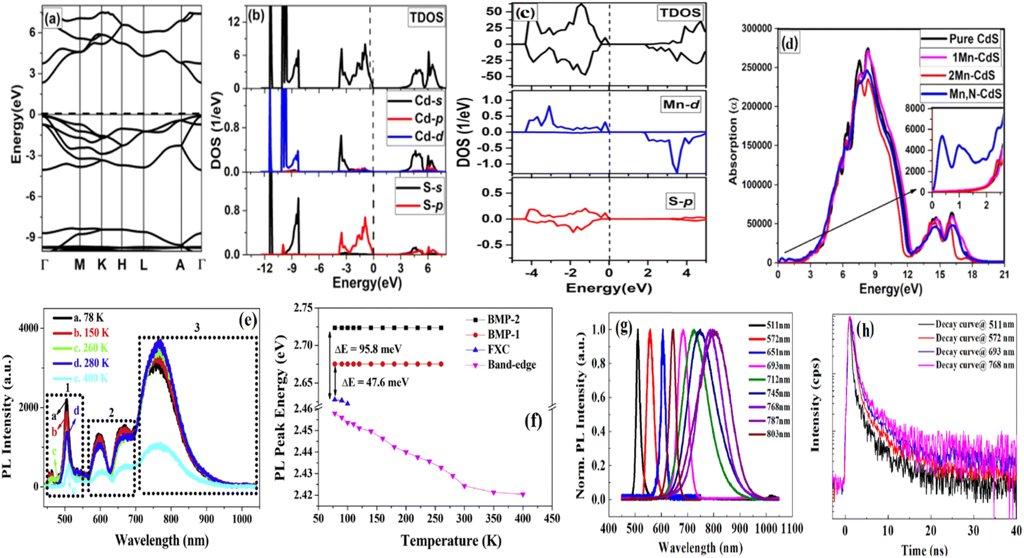 | ||
| Fig. 2 (a) Calculated band structure and (b) TDOS and PDOS of pure CdS. (c) TDOS and PDOS of Mn-d, S-p and N-p for FM configurations in Cd34Mn2S36. (d) Calculated optical absorption coefficient for pure CdS and Mn-doped CdS with and without N co-doping.95 (e) Temperature-dependent micro-PL spectra in the bright-field optical image of an individual Mn-doped CdS nanosheet. (f) Temperature-dependent PL peak positions of the band-edge for CdS (purple), FXC (blue), BMP-1 (red), and BMP-2 (black) in the Mn(II)-doped CdS nanosheet. (f) AFM- and FM-coupled Mn ions in CdS.107 (g) PL spectra of the obtained single undoped CdS and Mn2+-doped CdS belt at 300 K. The black line is from the pure CdS belt and the other lines are from the emission of CdS doped with different Mn ions. (h) PL lifetime decay plots for the band-edge emission together with Mn2+-related emissions at room temperature in an Mn-doped CdS single belt excited at 405 nm.102 | ||
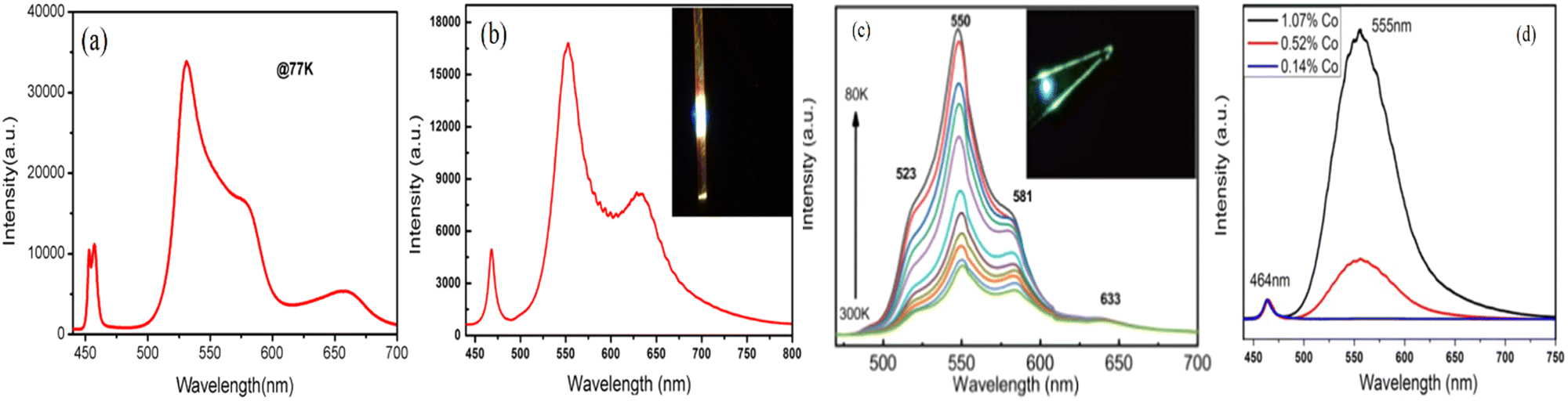
Fig. 2g shows the PL spectra of 1D belt-like structures of both undoped and Mn(II)-doped CdS and Mn(II)-doped synthesized by the VLS mechanism. The undoped CdS shows a strong near-band edge emission at 508 nm and no emission peak after 525 nm.5,102 In the case of the Mn-doped samples, their luminescence spectra show emission bands in the range of 570–900 nm, besides their bandgap emission, as shown in Fig. 2g. The appearance of multiple emission peaks in their emission spectra is due to the d–d transition in the ferromagnetic (MnS)n cluster. The emission peaks at 510 nm and 518 nm in the doped sample are due to EMP, as also reported for a nanocrystal (NC) by different research groups.104–106 Therefore, the tunable emissions with different Mn ions in 1D CdS NBs make them interesting for various DMS applications. These emissions are attributed to the interaction between the free excitons and ferromagnetic cloud, as previously reported in other II–VI materials.97 The yellow band emission at 572 nm is attributed to Mn2+, which has been reported to be located in the range of 576–598 nm and is assigned to the d–d transition between the 4T1 excited state and the 6A1 ground state of Mn2+. Besides the band edge, other emission peaks also appear independently under a 532 nm excitation source below the band edge with the presence of a near band edge emission at 515 nm upon 405 nm excitation. This tunable emission owing to the Mn interaction with the host material has rarely been reported for DMS structures.8,103 Thus, the ferromagnetic exchange in this (MnS)n cluster has strong coherent coupling between magnetic ions within the lattice, which may lead to the formation of localized exciton magneton polarons because of the p–d hybridization and FM coupling.108–110Fig. 2h shows the PL decay curves for 1D CdS with TM ion doping excited at different wavelengths (405 nm and 532 nm) to understand the Mn2+ transition with the host CdS crystal symmetry.102 According to the PL decay curve, we can understand that the small change with a few nanoseconds (ns) smaller than the free exciton lifetime indicates that it is related to the combination of free excitons and EMP in Mn-doped CdS and the large change is due to the presence of inhomogeneous states (defects) in the structure. However, the steady changes in lifetime in the same direction indicate the that the emission spectra in the red to near IR region are related to the Mn ion and no defect-related states are involved in the bands. A further increase in excitation power will reduce the lifetime due to the interaction of more spin states and large coherent coupling.111–113 Therefore, this lifetime in the range of 1 ns reveals the reflection of spin–spin interaction during lattice relaxation, as reported in other II–VI semiconductors. Fig. 2e shows the luminescence spectra of an Mn-doped CdS nanosheet, highlighting the three different emission spectra in the range of (1) 440–550 nm, (2) 560–680 nm and (3) 700–1050 nm. The emission spectra in the range of 440 nm to 550 nm (green emission) at 78 K can be subdivided into triplet emissions owing to the splitting of the valence band into three sub-bands. According to the crystal field symmetry, the spin–orbital interaction of excited electrons can occupy three exciton energies [A-exciton (2.5535 eV), B-exciton (2.5675 eV) and C-exciton (2.629 eV)].107,114,115Fig. 3f confirms the existence of a band edge emission, free exciton emission and spin-exciton interaction at low temperature. Moreover, the band-edge peak emission as a function of temperature is mainly observed in wide bandgap semiconductors.
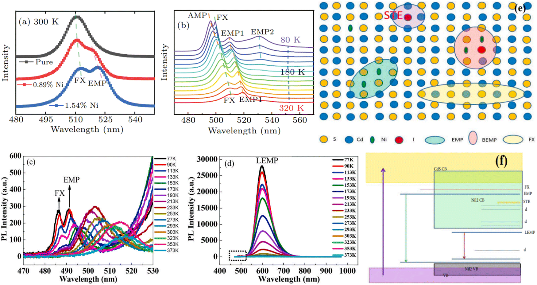 | ||
| Fig. 3 (a) Micro-PL spectra of CdS NB at different Ni concentrations in the range of 480–550 nm at RT. (b) Temperature-dependent micro-PL spectra of CdS NB with Ni concentration of 1.54% in the range of 470–570 nm.98 (c) Temperature dependence of PL of single Co-doped CdS NB excited with CW laser at 405 nm. (d) Magnified selected spectrum in the range of 470–530 nm, as marked by a rectangle.5 (e) Spatial distribution diagram of the different excited states in NiI-doped CdS lattice. (f) Electronic structure of CdS:NiI2 NB, in which the nanocluster of NiI2 is incorporated.116 | ||
Ge et al. reported the coherent bosonic lasing of EMP at 520 nm at 232.393 μJ cm−2 for Ni-doped CdS synthesized via the VLS mechanism.98Fig. 3a and b show the room temperature PL spectra of doped and undoped CdS and a low temperature for an Ni concentration of 1.54% in CdS NB, respectively. In the VLS mechanism, the S vacancies are normally generated during the growth of a 1D system in the presence of hydrogen in the source gas. In the case of Ni2+-doped CdS, the dopant atom substitutes the Cd ion at a higher concentration but this may not happen for a low doping concentration.114,115,117 Another important discussion is the crystal symmetry of the host material and dopant ion interaction with the crystal symmetry. Under luminescence, the transition of the carrier excitation and de-excitation/recombination will provide detailed information about the spin-carrier interactions in semiconductors. Therefore, the EMP-related peak in Ni-doped CdS will become dominant with an increase in the dopant concentration, which is directly correlated with the coupling of the dopant cation in the crystal symmetry. In the case of the pure CdS belt-like structure, the redshift in its PL spectra is owing to deficiency of S ion during its growth, which may lead to the formation of donor levels in the conduction band. Consequently, the dopant ion incorporated in the CdS lattice will induce more defects within the host lattice, which may produce strong exchange interaction with the spin magnetic ions with native defect states.115,117,118 This strong exchange interaction produces a broad EMP emission or redshift at room temperature. Ge and co-workers reported an increase in the intensity of the free exciton and EMP emission ratio. The lattice shrinkage may weaken the electron–phonon interaction at low temperature. At 80 K, different peaks appear in the emission spectrum, corresponding to free excitons, EMPs and antiferromagnetic magnetic polarons of Ni2+ pairs. Moreover, the bosonic lasing of EMPS condensates out of complicated states upon excitation by a femtosecond (fs) laser, as reported in other II–VI 1D nanostructures.3,117 The spectra ranging from the red to near-IR region originate from the FM coupling with the Mn clusters become prominent at a temperature lower than 260 K owing to the localized EMP, as observed in Mn-doped CdS. The same behavior of EMP formation has been observed in ZnSe Co-doped NWs. However, the lowest transition level for Co-doped CdS exhibits p–d hybridization through the high 3d state, which normally possesses a longer lifetime.118 The low-temperature luminescence spectra of Co-doped CdS reveal strong free exciton, EMP and LEMP emissions, as shown in Fig. 3c and d. The TM in the host material also results in a red shift in the band edge and LEMP emissions due to the high level of d–d transitions from 4T1 (P) to 4A2 (F) of the Co ion.5,119–121 When the temperature is lower than room temperature, the slight blue shift in the intra-shell d–d transition emission in the emission spectra implies that the d–d transition in Co-doped CdS is less localized than that in the Mn-doped CdS lattice. Based on the VLS mechanism, various studies highlighted the successful incorporation of TM ions in 1D CdS NWs and NBs, which exhibit room temperature ferromagnetism and anti-ferromagnetism. Ni-doped CdS crystals also exhibited a broad EMP emission at 600 nm, which is attributed to the d–d transition of 3T1(P) to 3T1(F) of the intrinsic Ni(II) ions in sulfide. Gaussian fitting of the broad EMP emission based on experimental data for Ni(II) doped in CdS revealed that the cubic crystal field may split due to the reduced symmetry information; therefore, the broad emission in Ni-doped CdS is due to its two-level emission, which is difficult to distinguish in comparison with the Mn-doped CdS nanostructure synthesized via the VLS mechanism.107,109,113Fig. 3e shows single Ni and I and coupled Ni + I doping in the host lattice, resulting in an inhomogeneous DMS structure. Fig. 3f shows the ion doping-related electronic structure of CdS:NiI2 NB. The EMP emission observed very far from the CdS:NiI2 band edge emission owing to the high magnetic ion concentration or defect formation due to F or Cl during growth via the VLS mechanism in the presence of hydrogen in the source gas. Meanwhile, Br or I ions are heavy and may be co-doped with Ni in the host lattice, exhibiting strong lasing phenomena, which will be detailed discuss in the lasing section. The co-dopant ion in the CdS lattice may lead to the formation of exciton complexes or acceptor/bound excitons or self-trap excitons, as shown in Fig. 3e, which have different exciton spatial distributions within the lattice.114,120
High-density EMPs can polarize and combine with the free excitons in 1D NB of CdS:Co, leading to coherent emission behavior at room temperature. EMP condensation in NB happens due to the following reasons: (1) spin coupled with excitons and phonons; (2) spin ion aggregation with FM coupling; (3) EMP is more stable than free excitons in materials having a higher exciton binding energy than thermal energy, which are coherently coupled through FM exchange interaction; and (4) the 2LO phonon along the c-axis in a hexagonal structure has a large transition probability and strong polarizability to interact with excitons, favoring the EMP state in TM-ion doped semiconductors. Due to its weak interactive force, highly stable spin–exciton–phonon (LO phonon) polarization may exhibit a bipolaron emission in the PL spectrum at high temperatures. Moreover, the much lighter effective mass of excitons than electrons in the CdS:Co semiconductor results in their strong interaction with EMP condensation at a critical temperature. The steady-state spectrum exhibits a two-band emission near the bandgap, which is related to the free excitons and EMP at room temperature, as shown in Fig. 3c, for 1D NB of Co-doped CdS. The second peak (518 nm) is very close to the 2LO A1 phonon, which indicates that EMP formation close to the band edge requires phonon polarization in the same direction. Therefore, the orientation-dependent EMP collect free excitons to condense and produce a lasing emission even in the perpendicular direction. This coherent EMP condensation resulting in lasing in II–VI 1D structures needs to be studied under ns laser excitation for a better understanding of the exciton–exciton, exciton–electron, exciton–phonon and exciton–spin interactions on variable timescales.100,122 The spectral line width and intensity are strongly dependent on the excitation power of Co-doped CdS. In the case of the threshold power of 7.4 μJ, the linear increase in intensity is due to the inhomogeneous distribution of magnetic ions in the belt. Alternatively, for a threshold power of 16 μJ, the lasing line width and intensity are not very wide due to the exciton–carrier or exciton–phonon interaction, which may involve lasing in single structures. This random lasing in 1D structures depends on the exposed area, which is helpful to understand the collective EMP lasing phenomena in doped wurtzite microstructures.100,123 The collective EMP condensation favored by the 1D longitudinal polarization and FM coupling of magnetic ions can be detected at room temperature for a better understanding of the magnetic exciton BEC in DMS nanostructures. The exciton magnetic polaron states in 1D NB and NW appear due to the exchange interaction between the spin–carrier interactions, resulting in the formation of EMPs. The overlapping tails of the carrier wavefunctions and spins result in large cluster formations under a high excitation density and respond as collective magnetic polarons to pronounce the bosonic nature in NWs and NBs. Therefore, the collective EMP condensate due to coherent light in nanostructures shows photo-magnetism behavior, which increases the possibility of modulating single-mode lasing by FM coupled with exciton in DMS. The large EMP coherence space and optical or magnetic modulation in the 1D nano/microstructure of wide bandgap semiconductors need further study for their nanophotonic application in future devices.5
3.1.2.1 Transition metal ion-related luminescence behavior. To understand the lasing phenomena in the CdSe matrix, it is important to determine its spatial recombination through spectroscopic measurements. CdSe NC has a poor band edge emission, which is attributed to two main reasons, as follows: (i) the optically inactive state at the bottom of its conduction band, which is known as dark exciton and (ii) transition from defects to the valence band. Interestingly, in the case of 1D nanostructure CdSe synthesized via the VLS mechanism, it exhibits strong luminescence at high excitation, which may increase the population rate at the lowest conduction band level. Alternatively, high crystallinity was achieved in the hexagonal CdSe nanostructure obtained via the VLS mechanism, which exhibited the red color lasing line of individual crystalline CdSe NB, as reported by Pan.130,134,135 Meanwhile, the size-dependent and lateral thickness of the CdSe nano-platelets tuned the LO–phonon corresponding to low exciton–phonon coupling, large oscillator strength and energy spacing of both. The optical transition energy related to the exciton–phonon interaction in CdSe was controlled by its lateral size and thickness by Achtshein.131 CdSe platelet-like structures are attractive for optoelectronics and enable control of the exciton energy states based on their thickness; however, their lateral dimension disparity in LO–phonon coupling is independent of their thickness and lateral size.
Another major key feature of II–VI materials is that heavy anions in the crystal field offer a low optical phonon energy cutoff value and reduce the efficiency of non-radiative decay. This decrease in efficiency provides the potential to realize a high fluorescence yield at room temperature, as shown in Fig. 4a.133 Yu et al. synthesized CdSe nanoplatelets and nanoribbons doped with Mn2+ ions using the solution process mechanism, as shown in Fig. 4b.136 TM ion doping in CdSe in low-dimensional systems (NWs, nanoribbon, etc.) results in unique magneto-optical behavior, as characterized by various spectroscopic analyses. Mn2+ doping in CdSe results in strong carrier-induced ferromagnetism due to the sp–d exchange interaction between the magnetic ion and electronic state of CdSe. Thus, quantum confinement at the nanoscale provides dominant carrier–spin exchange interactions and opens new horizons in the field of DMS.137–141 Mikulec and Erwin reported that the incorporation of Mn2+ in ZnSe and CdS is comparatively more convenient than in the CdSe matrix. The probability of Mn ion doping in the CdSe matrix is 50% for its bulk, whereas in its NC, it is still challenging.142,143 The surface adsorption of magnetic ion impurities during the nucleation process at the nanoscale results in the formation of clusters, which known as magic-sized clusters suitable for uniform doping in the host crystal. In the case of nanoscale or 1D nanostructures, a reduction in their dimensions may increase the possibility of quantum confinement and provide a low probability of impurity ions adsorbed within the magic-sized cluster. Yu et al. successfully doped Mn2+ ions in CdSe NC, as shown in Fig. 4b.136,144 Magnetic ion doping in magic-sized cluster formations during the nucleation stage of growth provides a uniform doping concentration in the host semiconductor. Cu2+, Ag2+ and other TM ions have been successfully doped in NC, exhibiting a red-shifted broadband emission at room temperature. Pan et al. prepared hexagonal CdSe NW- and NB-like structures via the CVD method, which exhibited red-color lasing within individual nanostructures.130 Chen et al. also prepared a 1D CdSe nanostructure via the CVD method, which exhibited strong excitonic behavior at different temperatures, as shown in Fig. 4c–e.145 Its temperature dependent absorption spectra at 10 K show that the strong emission spectra of the exciton peak (1.8248 eV) and free exciton peak coincide with the LO phonon (1.8515 eV) of CdSe NWs. Due to lattice expansion, the low temperature mapping of CdSe NWs strongly exhibits the exciton–phonon interaction. According to the Bose–Einstein approximation, the exciton–phonon interaction function of temperature and low temperature variation is very helpful in analyzing the thermal expansion and exciton–phonon interaction due to bandgap shrinkage. Similarly, the temperature-dependent luminescence spectra show an increase in intensity at low temperature and the inset image in Fig. 4e shows the difference in activation energy (5.40 eV and 18 meV), as calculated using the dual activation energy model, where the energy of 18 meV is comparable with the bulk exciton energy.145,146 According to the crystal field theory, the ground state of the Cr2+ ion is 5d to the upper levels in the visible spectrum. The tetrahedral site of the crystal field (Td) splits 5d into triplet (5T2) and doublet (5E) states. In the case of Cr2+, the triplet state allows the transition between levels and the allowed spin state, whereas in the case of Fe2+, the doublet state allows the transition in the host matrix. Therefore, the Cr2+ ions can undergo a transition from 5E (5d) to 5T2 (5d), which is promising for laser application. The John–Teller mechanism and spin–orbital coupling are also responsible for the energy splitting. Numerous reports have shown that Cr2+-doped CdSe exhibits direct lasing at room temperature. Similarly, Chen et al. showed that a change in the excitation density will enhance the spontaneous emission; therefore, multiple peaks appear at 715 nm and 725 nm (above the threshold value of 0.296 MW cm−2) at room temperature. These multimode random lasing in a single structure of CdSe NW in the NIR region make it suitable for NIR optoelectronic applications such as sensors, lasers and energy conversion devices.133,147,148
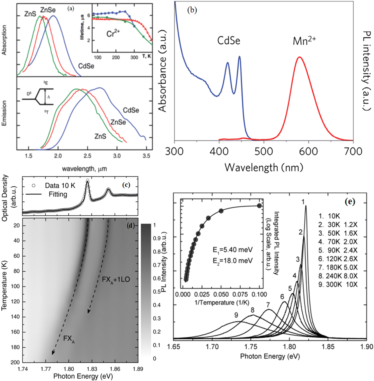 | ||
| Fig. 4 (a) Normalized room temperature absorption and emission-gain spectra of Cr2+ ions in ZnS, ZnSe, and CdSe crystals. Inset shows the temperature dependence of Cr2+ ion lifetime in ZnS (circle), ZnSe (triangle), and CdSe (square) crystals; Copyright © 2010, Wiley InterScience.133 (b) Absorption (blue line) and PL (red line) spectra of Mn-doped CdSe NPLs; Copyright © 2009, Springer Nature.136 (c) Low temperature (10 K) free-exciton absorption of CdSe NWs. The solid curve is the multi-Gaussian fitting of the absorption spectrum. (d) Temperature-dependent mapping of the absorption spectrum. (e) Free-exciton emission of CdSe NWs at various temperatures. The inset plots the dependence of the integrated PL intensity on the reciprocal of temperature, and the solid curve is the Arrhenius fit with two activation energies, Copyright © 2011, Wiley.145 | ||
Solution-processed colloidal QDs exhibit exciton and bi-exciton lasing at room temperature. Their spectral symmetric PL is temporally integrating the streak image over the nanosecond fitted by the pseudo-Voigt function for low and high fluence provide information related to their exciton and bi-exciton transition. The giant oscillator strength near the band edge emission has strong coherent phasing strength, as correlated with a single atom in the host matrix. Therefore, ultrafast dynamics spectroscopy provides detailed information of the carrier and decay kinetics in the picosecond (ps) domain. The bi-exciton lifetime of the CdSe matrix is dominated by non-radiative Auger recombination up to 10 ns, which is almost the two order of magnitude larger than the measured radiative lifetime. The streak camera images of a CdSe CQ well excited with 1 kHz, 70 fs laser pulses and fluence of 20 μJ cm−2 with the ultrafast time decay measurement value about ∼10 ps unambiguously assigned the peak to the stimulated emission, providing evidence that the intensity-dependent spectra originated from the bi-exciton transition within the respective energy position at an ultralow threshold fluence.149
3.1.3.1 Transition metal ion-related luminescence behavior. Various researchers have extensively reported TM ion doping in CdTe for DMS and optoelectronics applications such as solar cells. TM ion doping in II–VI materials is related to the 4d element effect on both optical and electrical properties. Kurchatov and others research reported the successful incorporation of TM ions within the II–VI host matrix, which exhibited IR lasing emission at room temperature.155–157 Lafuente-Sampietro et al. reported the resonant optical control of the spin (single Cr atom) in CdTe/ZnTe QDs.158,159 At 5 K, the Cr spin relaxation was observed by a strong resonant laser field, which is responsible for the Cr atom tuning optical Stark effect. The circular polarized PL spectra of the magnetic anisotropy of the Cr spin were induced by biaxial strain. The exchange interaction between the spin atom and exciton further splits the Cr energy level due to the high polarizability of the crystal field. To understand the carrier dynamics in CdTe/ZnTe QDs doped with Cr atoms, a pump probe experiment was performed to observe the relaxation time and non-equilibrium distribution of the Cr spin population with a circularly polarized resonant pump pulse. The peak intensity map of Cr doped in CdTe/ZnTe QDs showed the low energy bright exciton state and dark exciton. The Cr ion interaction with phonons in the system shows strong spin–phonon coupling at low temperature, which is an important step forward to control the TM ion coherent spin for future spintronic devices.158,160 Similarly, the Cr spin is coupled with excitons near the valence band and shows nano-magnetic behavior due to the optical pumping of electron-Cr and hole-Cr. Resonance and non-resonance optical pumping can be directly used as spin memory (write and erase, respectively). Therefore, the spin channel can be studied with polarized emission, which responds to the relaxation channel of the Cr ion in II–VI semiconductors. Therefore, the optical pumping- and power-dependent PL intensity-related temperature effect is directly affected by the hole-Cr spin near the valence band and electron-Cr local generation of phonons.
Optical pumping shows the positively charged exciton and relaxation of Mn-spin exchange coupled with confined hole spin in CdTe. This spin can be observed under the optical injection of spin-polarized carriers in the time domain of a few tens of ns. Interestingly, the localized spin state can be controlled by the charged state of strain-free QDs. Thus, the magnetic anisotropy of an atom can be controlled by an electrical field, making it suitable for miniaturized data storage application for fine structure and strain-free QDs. This fine structure shows the spin splitting of the Mn ion in the energy range of a few meV coupled with heavy-hole spin near the valence band of CdTe. Pumping and a magnetic field influence the Mn-electron dynamics in the excited state and Mn-hole in the ground state. In the case of zero magnetic field, the spin-relaxation time of the Mn-hole is shorter due to valence band mixing.157,159–161 PL time delay measurements can further explain the dynamics of charge carrier interaction with the optically active injection of spin polarized photo-carriers. Similarly, Mn doped in CdTe QD shows a spin flip under resonant excitation, which is mainly controlled by the carrier–spin interaction. This coherent dynamics is directly observed in the ultrafast time domain and localizes the spin ion in the CdTe matrix.157,159–161 The Bose–Einstein condensation (BEC) of the exciton–polariton-related phase transition is related to the quantum effect in the CdTe/CdMgTe microcavity at 5 K.162 The spontaneous quantum degeneracy of polaritons in the CdTe microcavity excited by non-resonant pumping significantly narrows the polariton emission line width. The condensation of exciton polaritons in CdTe-based microcavity condensation is not standard BEC due to leakage in the cavity. The polaritons are non-interacting as bosons but do not follow the conservation law above some critical density at a specific temperature. Accordingly, the spatial coherence and macroscopic polarization through condensation can be used as a polariton-laser in CdTe. Thus, for wide bandgap semiconductors such as ZnO and GaN, the polariton condensation builds macroscopic polarization and spatial coherence for polariton lasers with an increase in temperature.162–165
A Cd-based ternary alloy CdSexS1−x NW with a homogenous composition was synthesized through a solution–liquid–solid process by Yang and co-workers.58,176 Ternary alloy nanostructures have attracted significant attention owing to their continuous tunable bandgap, making them suitable for various electrical and optical applications such as photodetectors, solar cell, and FETs. Rosenthal et al. reported the ternary NC of CdSexS1−x having different sizes and compositions; their results indicated that the surface states are strongly correlated with the relaxation process of photo-excited carriers, as studied by ultrafast fluorescence upconversion spectroscopy.176–178 Colloidal CdSexS1−x NWs exhibit strong emission, which can be tuned in the range of 508 nm to 628 nm with a narrow spectral width together with a high quantum yield. Therefore, the tunable and polarized emission of CdSexS1−x NWs provides greater insight to understand the exciton dynamics for various optical applications, as shown in Fig. 5a–d. Fig. 5a and c show the absorption and PL spectra of CdSexS1−x alloy NWs, respectively, where the variation in the composition gradient shows a redshift in the bandgap tuning with an increase in the Se ratio. A similar study was conducted for CdSexS1−x alloy NWs synthesized via CVD, NCs and quantum dots (QDs).170,179–182 At low temperature PL, the defect-related emission of different compositions was suppressed except for CdSe and CdSe0.25S0.75, indicating that the formation of alloy CdSexS1−x NWs can be feasible for high-quality polarized LEDs, as shown in Fig. 5f. The spectral broadening of the emission can be related with (i) inhomogeneous broadening, (ii) optical phonon interaction and (iii) acoustic phonon interaction at low temperature. Alternatively, the bandwidth broadening can be related with (i) acoustic phonon scattering, (ii) longitudinal optical (LO) phonon scattering and (iii) exciton surface scattering. Below 130 K, for CdSe and CdSe0.25S0.75, the acoustic phonons contribute significantly (dotted line comes from inhomogeneous broadening and acoustic phonon scattering) but above 130 K, the LO phonon and surface phonon contribute more effectively and are responsible for the bandwidth broadening, as shown in Fig. 5e. According to their luminescence spectra, we can understand the recombination dynamics of photo-generated carriers with the help of a schematic diagram (Fig. 5g). This process can be described as follows: (i) photoinduced excitons can localize in the valleys, (ii) radiative recombination, (iii) generation of photoinduced excitons and (iv) surface defects and (v) trapped electrons recombine with trapped holes to produce defect-related emissions. However, both the compositional gradient of alloys and nanoscale dimensions strongly influence the exciton recombination due to the surface-induced quantum confinement, as reported in different studies.183–186 Therefore, PL decay measurement becomes an effective tool to analyze the recombination process at a very low excitation power. The preparation of CdSexS1−x ternary alloys via the CVD route was reported by Pan and other research groups, as shown in Fig. 5h–k.75,77,179 Liu's and co-workers also reported the preparation of CdSexS1−x alloy NWs for various applications such as sensors, thermoelectrics (Fig. 5l–o), wave-guides and photodetectors in recent years.187–189 Besides ternary alloys of II–VI semiconductors or heterostructures, radial core/shell nanostructures are also are important for bandgap engineering, which have attracted attention due to their special structural characteristics and miscellaneous applications such as field-effect transistors, solar cells, biomedical applications, and memory devices.25,69–71,190 In the case of type-II heterostructures of CdSeTe, wurtzite (CdSe) and zinc blende cubic (CdSe) structures can be achieved by controlling the temperature and ligand. Moreover, the Se and Te contents in heterostructures tune the bandgap-related emission, while the diameter and shape of tetrapods affect the emission linewidth.191 Low-threshold lasing for CdTe at the surface of core of NW or NC exhibited a strong lasing emission line. Colloidal type-II (CdSe/CdTe) heterostructures have minimal overlap of e–h wave function at the interface, which intensifies the amplified spontaneous emission with a high density of charge transfer and exhibits strong lasing at a lower threshold value.192 Interfacial type-II heterostructures lengthen the Auger recombination lifetime, which supports continued lasing, and the decrease in oscillator strength between electrons and holes will intensify the optical gain for LED and laser applications. Transient absorptions show the multiple oscillation at a high pump power assigned to acoustic phonon normally observed in single metal nanostructures with a quality factor of 9–10. The inhomogeneity of CdTe NWs lead to different charge carriers and charge trapping, which is related to the surface and pump power.193
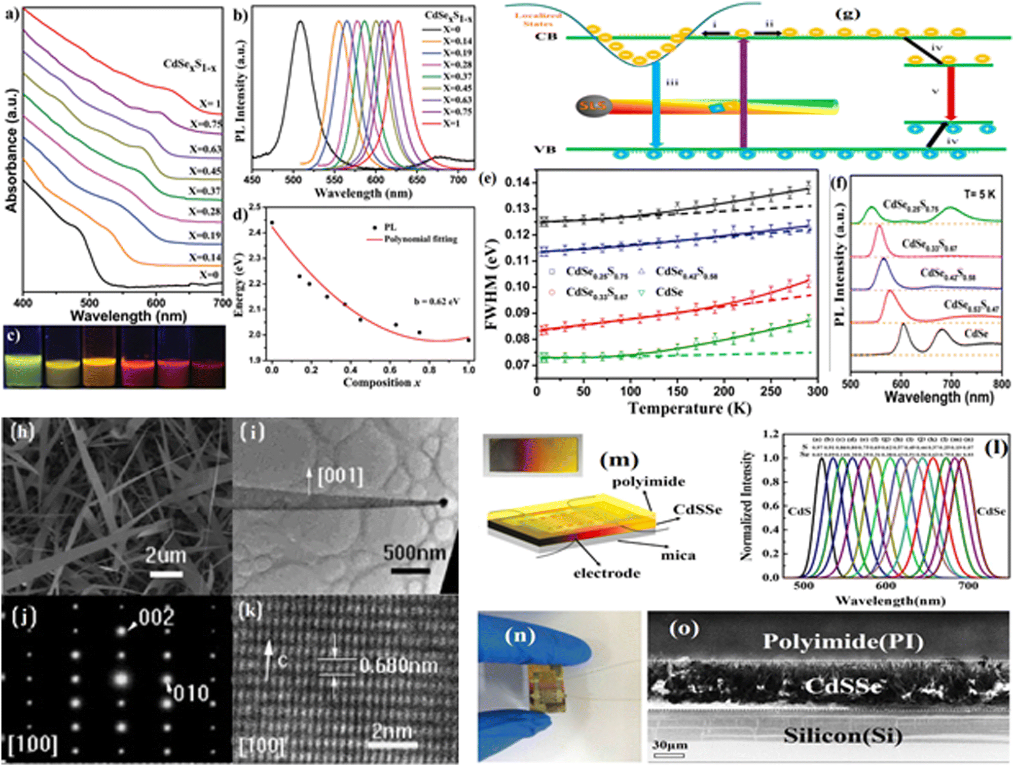 | ||
| Fig. 5 (a) UV-vis absorption spectra of CdSxSe1−x prepared via a solution process and (b) PL spectra of CdSxSe1−x NWs with different Se contents. (c) Photographs of typical emission colors from the obtained alloyed NWs under UV 365 nm irradiation. (d) Energy gap–composition correlation of CdSxSe1−x NWs, where the data points represent the value extracted from their respective PL.176 (e) Solid lines were fit using Varshni's law and the temperature-dependent exciton–phonon model, while the dotted line represents the inhomogeneous broadening and the acoustic phonon scattering. (f) PL spectra of varying compositions of alloyed NWs at 5 K. (g) Schematic of the kinetic model of exciton recombination in NWs.58 (h) SEM morphology of ternary CdSxSe1−x NBs synthesized by CVD; (i) TEM image; and (j) and (k) selected area electron diffraction (SAED) pattern and HRTEM image, respectively.70 (l) PL spectra measured at different composition along the length direction of a CdSSe NW. (m) Real-color photograph of CdS1−xSex chip and diagram of the sweat sensor and (n) real image of the as-prepared sweat sensor. (o) Cross-sectional SEM image of PI-coated CdSSe NW chip.188 | ||
Pan et al. synthesized an axial NW-like structure of CdS/CdSSe via the VLS mechanism. The pumping fluence exhibited two broad emissions at 520 nm (green emission) and 600 nm (red emission) at a low pump power of 29 μJ cm−2, corresponding to spontaneous emissions. Both emissions showed a sharp bandwidth of 0.4 nm at a high power, demonstrating the stimulated emission in the heterostructure. Moreover, the slight blue shift at a power corresponding to electron–hole plasma formation at the surface contributed to exciton–phonon scattering and red shift due to the bandgap renormalization effect.75,77 Guo et al. synthesized a high-quality ternary alloy of CdS1−xSex nanotripods for broadband tunable single-mode lasing and high integration optical circuits and photonics communication.173 Various factors such as the compositional variation and diameter of the tripod-related cavity had a prominent effect on tuning the band gap of CdS1−xSex and single-mode lasing. Therefore, their tunable wavelength has numerous applications such as wavelength-converted devices, nanophotonic lasers and optical communication on signal chips.123,194,195 Yang et al. also reported the bandgap tuning of colloidal NWs of CdSexS1−x synthesized via a solution process. At low temperature, their PL spectrum showed a surface defect-related emission, corresponding to the excitons and localization states based on the compositional ratio of the NWs. Therefore, the greater number of carriers localized in these states, which do not move to the surface, possible enhanced the radiative recombination in the ternary alloy.
The CdS/SnS2 superlattice microwire synthesized via CVD showed multiple emissions, which were modulated by the excitons and photons in the 1D system. The physical deposition method successfully achieves strong lasing for multicolor emission at a low threshold value. Novel multi-peak emissions with controllable periods were observed for the first time due to the contribution from the 1D photonic crystal and periodical exciton confinement.58,176 Sn doping in CdS not only tuned the bandgap emission but also changed the defect-related emission line. Peng et al. also observed the strong electron–phonon coupling interaction in the optical micro-cavity of CdS–Sn, which is associated with the interaction, trapping and recombination of carriers in 1D nanostructures.196 Tian et al. showed the effect of quantum confinement on the polarization anisotropy emission in CdS–Sn micro-cone-like structures. The polarization ratio achieved reached 60%, providing suitable information about the quantum confinement and optical confinement in nanostructures related to the dielectric contrast upon the incorporation of Sn in the CdS matrix. Also, the decrease in the cross-section radius of the nanostructures was attributed to Sn doping and the reduction in the carrier lifetime. Moreover, the polarization ratio of the magnetic ion or spin ion corresponding to dielectrics is beneficial to study spintronic devices at room temperature.123,197,198 Bao et al. reported the single-mode laser of a CdS NW channel on an SiN waveguide chip with high efficiency of up to 58% by evanescent coupling. The composition gradient demonstrated various emission colors ranging from green to red, while the lasing emission wavelength ranged from 520 nm to 738 nm, providing broad wavelength tripod lasers.199 Li et al. reported the multiphoton pump lasing of bi-excitons from a solution of colloidal CdSe/CdS nanoplatelets.200 The colloidal solution showed the optimal lateral size, which minimized the ultralow threshold for lasing at room temperature. CdTe alloys with other optical active materials such as CdSe as a type-II semiconductor tetrapod structure or ZnTe exhibit a strong optical response and are useful in various optoelectronic applications. 1D NW of CdS/CdSTe/CdTe showed high optical responsivity due to the n-type and p-type characteristics of CdS and CdTe, respectively. CdSTe acts as the depletion layer, which is similar to intrinsic silicon acting as sandwich in a PIN photodetector. Light illumination will transfer the photoelectrons from CdTe to CdS and transfer holes from CdS to CdSTe simultaneously, and then to the CdTe shell layer. The CdSTe layer reduces the carrier recombination probability and increases the photocurrent, making it suitable for photodetection in a wide spectral range.201,202
Fig. 6a and b show the lasing in CdS NBs co-doped with 0.1–0.68% Co(II) and prepared via CVD. The two-band emission near the band-edge is located at 508–510 nm (FX) and at 518–525 nm for the EMP at room temperature. YAG:Nd (355 nm using a 2 ns laser) showed a lasing line at 518 nm (Fig. 6a). Fig. 6b shows the line width and intensity as a function of excitation power. Beyond the threshold power of 7.4 μJ, a super-linear increase in the emission intensity can be seen. Regardless of the inhomogeneous distribution of the dopant ions in NBs, a single lasing mode always occurs at the EMP location. Over 6 μJ, the exciton–carrier or phonon interactions start and become involved in the lasing process. The Co(II) ions with ferromagnetic coupling provide significant carriers and driving force to complete this collective emission process, as observed in other II–VI semiconductors. Other II–VI semiconductors doped with TM ions and excited by a fs laser exhibit an EMP lasing line, whereas CdS:Co NBs show lasing with both ns and fs lasers. This difference indicates that the EMP in the latter should have a larger coherence length and coherence time because ns laser excitation can cover more microscopic interactions, such as exciton–exciton, exciton–phonon, exciton–carrier, and exciton–spin, inside the excitation zone, while these interactions usually exist in variable time scales.3
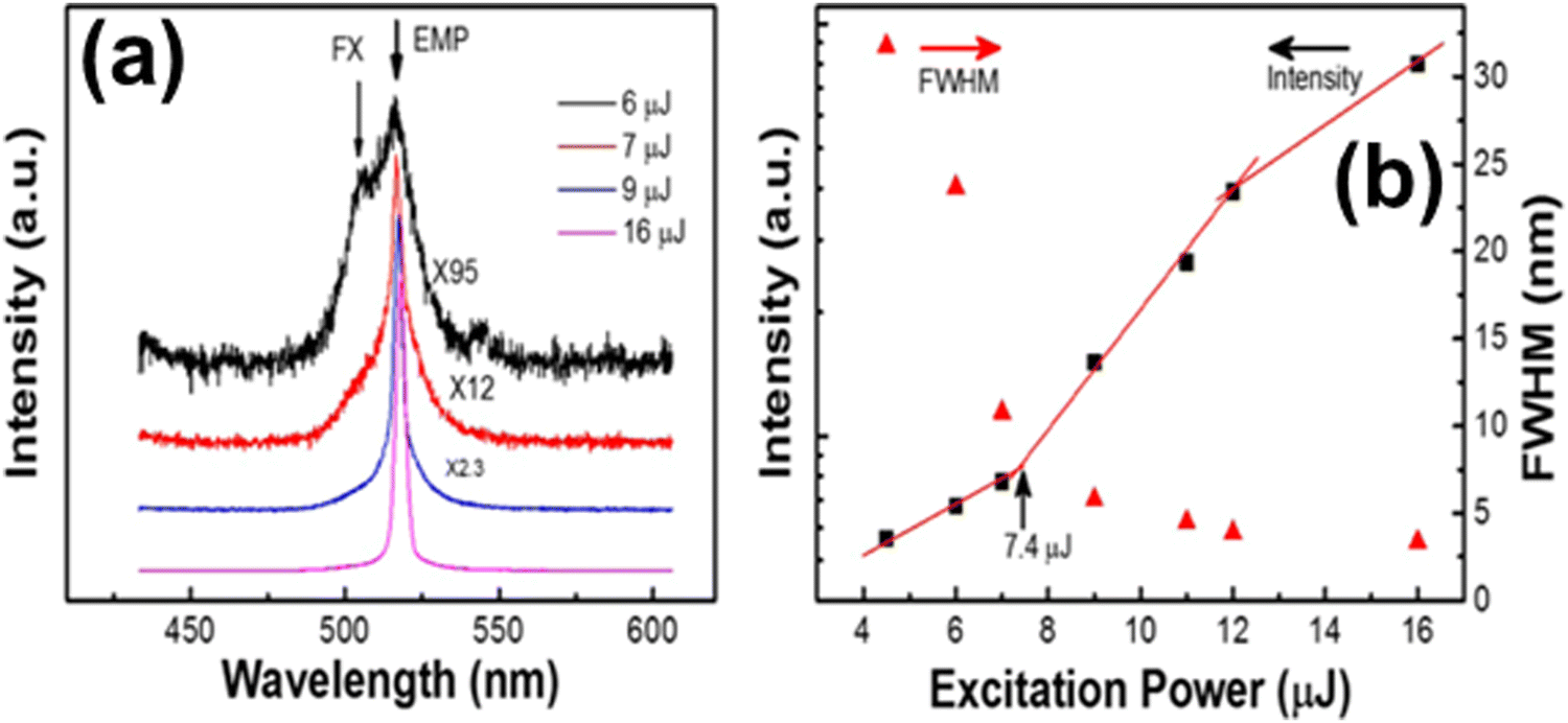 | ||
| Fig. 6 (a) PL spectra from spontaneous emission to stimulated emission when excited by a nanosecond pulse laser (355 nm). The PL emission intensity and FWHM were extracted and plotted as a function of pumping power. (b) When the excitation intensity was below the threshold, a broad spontaneous emission band was observed, which showed a linear increase with excitation power, while when the pumping power was larger than the threshold, the emission intensity showed a super-linear increase with the excitation power. Moreover, the width at half-maximum (FWHM) became narrower an increase in the pumping power. Copyright © 2016, ACS Publications.3 | ||
The type-II interface of ZnTe/CdSe reveals a significant blue shift toward a lower energy band, whereas the high-energy band is related with CdSe. The relatively small lattice difference between two semiconductor core–shell nanostructures with a high surface-to-volume ratio is suitable for photovoltaic applications.171,190,203 Wang et al. demonstrated that CdSe/CdS/ZnS QDs with a spherical optical cavity propagated the light around their circumference due to the ZnS shell at room temperature.204 The ratio of S![[thin space (1/6-em)]](https://www.rsc.org/images/entities/char_2009.gif) :Se in CdSeS NW could be controlled by the exciton dynamics together with bandgap tuning, as measured by fs transient absorption spectroscopy. The lifetime measurement showed a shorter wavelength with an increase in the Se ratio, while an increase in the S ratio revealed a large redshift in the steady-state absorption. The short time of about 10 ps with an increase in the Se ratio also revealed the photo-bleaching recovery from 8.4% to 57.7%, making CdSSe 1D NWs suitable for photovoltaic and optoelectronic applications with good control of both their optical and excited state properties. The homogeneity of an alloy depends on the phonon frequencies of the atomic mass in the unit cell and lattice configuration. A change in the S:Se ratio resulted in a linear shift in the Raman bands of the LO phonon frequency to a higher or lower wavenumber. The Raman bands of CdS and CdSe show the homogenous distribution of Se and S atoms in QDs together with new Raman bands between the LO phonon frequency, showing the breaking of the translation invariance in the lattice. The additional vibrational peaks show the presence of an isotope mixture near the center of the optical mode, which is correlated with the linear frequency-mass dependency in the crystal system.170,182,183,205–207 In the case of QDs, the size-dependence broadening of their Raman lines due to phonon confinement, while the weak confinement and narrow bandwidth distribution result in a sharp Raman line due to the uniform or homogeneous distribution of the precursors.
:Se in CdSeS NW could be controlled by the exciton dynamics together with bandgap tuning, as measured by fs transient absorption spectroscopy. The lifetime measurement showed a shorter wavelength with an increase in the Se ratio, while an increase in the S ratio revealed a large redshift in the steady-state absorption. The short time of about 10 ps with an increase in the Se ratio also revealed the photo-bleaching recovery from 8.4% to 57.7%, making CdSSe 1D NWs suitable for photovoltaic and optoelectronic applications with good control of both their optical and excited state properties. The homogeneity of an alloy depends on the phonon frequencies of the atomic mass in the unit cell and lattice configuration. A change in the S:Se ratio resulted in a linear shift in the Raman bands of the LO phonon frequency to a higher or lower wavenumber. The Raman bands of CdS and CdSe show the homogenous distribution of Se and S atoms in QDs together with new Raman bands between the LO phonon frequency, showing the breaking of the translation invariance in the lattice. The additional vibrational peaks show the presence of an isotope mixture near the center of the optical mode, which is correlated with the linear frequency-mass dependency in the crystal system.170,182,183,205–207 In the case of QDs, the size-dependence broadening of their Raman lines due to phonon confinement, while the weak confinement and narrow bandwidth distribution result in a sharp Raman line due to the uniform or homogeneous distribution of the precursors.
3.2 TM ion doping in zinc chalcogenides (ZnX; X = O, S, Se, or Te)
3.2.1.1 Transition metal ion-related luminescence behavior. Fig. 7 shows the PL spectra of different TM ion-doped (Mn2+, Ni2+, Co2+, and Fe3+) ZnSe nanostructures.20,117,213,216 Mn-doped ZnSe nanostructures have been synthesized via the VLS mechanism and solution process, as reported by many researchers.20,217–219Fig. 7a shows the PL spectrum of Mn-doped ZnSe nanoribbons, where the peak at 461 nm is assigned to the near band edge emission at room temperature. At 77 K, the peaks split into two bands, originating from the free excitons and EMP. The emission peaks at 534 nm and 646 nm correspond to the low energy side and high energy side of the d–d transition (D1) originating from 4T1(4G) → 6A1(6s) in Mn-doped ZnSe. The emission peak at 585 nm is related to the d–d transition. The d–d transition of Mn in ZnSe has been extensively reported in other II–VI semiconductors. In the case of ZnSe as the host matrix, the peaks at 534 nm and 650 nm corresponding to Mn can be attributed to the following: (i) Mn–Mn ions aggregate to form AFM coupling, (ii) self-activation of VZn–ClSe complexes due to Mn doping, (iii) direct coupling of FM Mn–Mn pairs and (iv) generation of surface trap states. Therefore, structural relaxation is involved in the optical emission of the Mn–Mn interaction pair in the ZnSe host matrix, crystal field and crystal lattice distortion to show the both FM and AFM pairs in the same zone. Therefore, low temperature PL provides sufficient information about the origin of the emission spectrum related to the Mn–Mn interactions in the host material. The emission peaks at 533 nm, 580 nm and 664 nm at 77 K are ascribed to the ZnSe emission related to the d–d transition and their small redshift is due to the sp–d hybridization effect. Fig. 7b shows the PL spectrum of Fe3+-doped ZnSe nanoribbons synthesized via the VLS mechanism, exhibiting three emission peaks at 467 nm, 553 nm and 630 nm.213 The peak at 467 nm is assigned as the band edge peak, as observed in Mn-doped ZnSe (461 nm; Fig. 7a). The emission peaks at 553 nm and 630 nm correspond to the second (D1) and third (D2) emission peaks related to the Fe3+ d–d transition, respectively. Moreover, the emission peak at around 467 nm under different excitations shows a redshift with an increase in intensity due to the following reasons: (i) bound excitons, (ii) EMP interactions and (iii) e–h plasma formation at the surface. In the case of low power, the bound exciton peak is dominant, while a further increase in power resulted in a red shift in the peak and increase in its intensity due to EMP. With a further increase in power, the emission peak reached 493 nm due to e–h plasma formation at the surface of the nanoribbon, which is related with excess charge of Fe3+. Therefore, low temperature luminescence and lifetime measurements provide suitable information about the emission spectra in the host matrix, as also studied by different groups.220–224
 | ||
| Fig. 7 Transition metal ion doping in ZnSe matrix. (a) Temperature-dependent PL spectrum of Mn-doped ZnSe nanoribbons excited with a CW laser (405 nm) at 77 K, Copyright © 2020, IOP Publishing.20 (b) PL spectrum of an individual Fe-doped ZnSe nanoribbon with a 405 nm laser upon excitation. The inset in the top right corner is the PL image of the nanoribbon in the dark field observation, Copyright © 2017, Applied Science.213 (c) Temperature dependence of the near-band-edge luminescence peak (FXs, EMPs) of NiI2-doped ZnSe NBs from 300 K to 80 K at relatively high (1.2%) doping concentration, Copyright © 2021, IOP publishing.117 (d) PL emission spectra measured at room temperature with different concentrations of Co-doped ZnSe NRs, Copyright © 2021, IOP Publishing.216 | ||
Fig. 7c shows the emission spectra of Ni-doped ZnSe at different temperatures.117 At 300 K, the two emission peaks appear at 463 nm and 471 nm, which are assigned to the bound excitons and EMP, as discussed for Mn2+- and Fe3+-doped ZnSe.225–228 At low temperature, the shoulder peak at 453 nm appears due to the incorporation of Ni ions; however, the combination of free excitons with AFM coupling with Ni ions or clusters resulting in the formation of this peak has rarely been reported in magnetically doped semiconductors.214,229–231 Hou reported that the incorporation of TM in ZnSe is the origin of its ferromagnetism, which may lead to a red shift in its emission spectrum. However, AFM coupling may lead to a blue shift in its emission spectrum when coupled with a d–d transition. Normally AFM coupling appears at a high doping ratio with bound excitons but is rarely reported with a low doping. Other studies on Ni-doped ZnSe also revealed the importance of DMS for future spintronics.232–234Fig. 7d shows the emission spectra of Co-doped ZnSe, which was prepared by Zou et al. via the VLS mechanism, exhibiting anomalous nonlinear optical behavior due to the incorporation of magnetic ions in the ZnSe nanoribbon-like structure. The PL emission spectra were recorded with a change in the Co doping concentration from 0.14% to 1.07%. It was observed that as the doping concentration increased, the intensity of the peak at 555 nm was enhanced due to Co–Co coupling. Thereby, the intra-shell with high d–d transition was responsible for the FM coupling of the TM ion pair, which may produce a nonlinear optical absorption. Moreover, the intensity ratio of the band edge emission and d–d transition can tune the visual emission under different doping ratios, as normally reported in NC.235–238
Lasing in pure ZnSe is attributed to its near-band edge emission, which is sharp due to the coherent transition without thermal distribution. Similarly, the spectra of Mn-doped ZnSe also exhibit lasing under different pump powers and the relationship between the excitation power and intensity was also presented. As the excitation power increased, the intensity ratio also increased in the nanostructure, exhibiting lasing in the doped sample. Normally, II–VI semiconductors doped with TM ions exhibit lasing in the NIR region.133,155,239–241 In addition, various studies reported that lasing is owing to the exciton–polariton within the microcavity formed in the structure during its growth or wurtzite structure.91,162 In the case of Mn-doped ZnSe NW, the two peaks in its emission spectrum at 466.8 nm and 472.5 nm are assigned to the bound exciton band edge emission and phonon-assisted exciton transition, respectively. A phonon-assisted exciton transition is possible when the excitons and phonons are coherent space or density of states and the same polarization may lead to the generation of a spontaneous polariton–exciton-related emission. In the case of the belt-like structure, the polariton–exciton emission has been reported at 475 nm with a broad emission at 650 nm related to the trapped-state emission.242 In the case of ZnSe:Ni nanoribbons, the free exciton lasing emission was dominant at a low excitation power, and as the excitation power increased, the EMP peak began to anomalously increase and became sharp. This anomalous behavior in doped ZnSe:Ni is owing to the nonlinear EMP-related lasing interaction with spin, LO phonons and excitons polarized in the same direction.117,230
3.2.2.1 Transition metal ion-related luminescence behavior. The total energy was calculated for both the spin and non-spin polarized states of ZnS NWs doped with Cr ions, as shown in Fig. 8(a)–(c). Cr(II) interacts with its nearest neighbor S atom by replacing a Zn ion. The p–d hybridization between Cr and S comes from the d-state and the p-states show a small magnetization. The spin density of states or distribution of Cr ions in ZnS NWs shows that the large contribution of the dopant ion to the total magnetization in the opposite direction favors the AFM interaction. According to the Bader charge (BC) analysis of the bond length and charge transfer, the doped NWs are stable due to the stronger Coulomb interaction between the S and Cr atoms than pure ZnS NWs. Moreover, the spin-down shows its semiconducting nature, whereas the spin-up shows that the half-metallic ferromagnetic semiconductor seems to be a good candidate for DMS spintronic applications. The FM state is stabilized through the spin-up of the Cr ion, which is partially filled due to the energy gain from the double-exchange mechanism, but the super-exchange mechanism has no energy gain. The spin-down of the Cr ion shows its semiconducting properties or absence of magnetism behavior. The exchange spin splitting of the d-orbital of Cr ions in the FM state is larger than that in the AFM state due to the double-exchange mechanism. Moreover, the intrinsic vacancy can be overcome by co-doping with non-metals such as N, C, and I at the anion site. The co-doping with N atoms contributes one hole to the valence band, which lowers the Fermi level close to the valence band. According to calculations, the total energy of co-doping at the surface is lower than that in the bulk, indicating that N prefers the surface of NW. In addition, the N-p states are asymmetrical in nature, which are involved in magnetization and favor the AFM coupling of the d-state with p-state of the N and S ions. Therefore, the co-doped atoms are involved in magnetization and the spin density is concentrated around the Cr and N atoms with a lower density around the S atom.
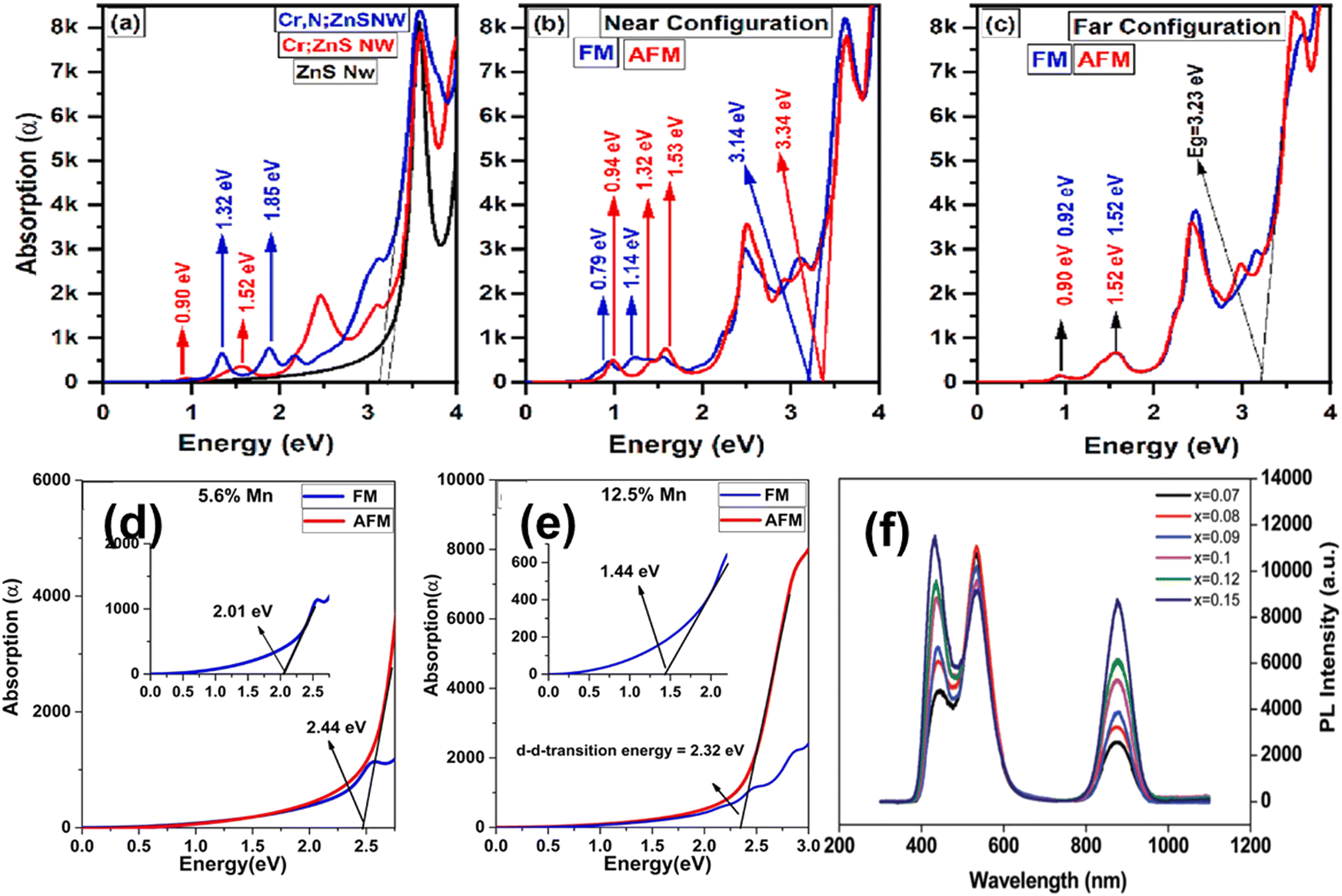 | ||
| Fig. 8 Optical absorption of (a) pure ZnS nanowire, single Cr(II) ion-doped wire, and single Cr and single N co-doped wires, (b) FM and AFM systems in near configuration, and (c) FM and AFM in far configurations, Copyright © 2023, Elsevier.256 Absorption spectra of FM and AFM coupled Mn ion-doped systems with 5.6% (d) and 12.5% (e) concentration of Mn dopants, Copyright © 2023 IOP, Publishing.257 (f) Room-temperature PL spectra of Zn1−xMnxS nanobelts, Copyright © 2017, The Royal Society of Chemistry.258 | ||
Fig. 8(a)–(c) show the absorption spectra of pure ZnS, the surface configuration of Cr ion and co-doped samples, which show high absorption in the near IR and UV-Vis regions. The surface-incorporated Cr ion showed the d–d transition energy of about 0.95 and 1.53 eV in the near IR region (Fig. 8b). The absorption peak at 2.42 eV corresponds to the transition between the d-state and p-orbital in the valence band. The peak located at 3.05 eV is attributed to the transition between the interband transition and d-states of the Cr(II) ion. Therefore, the Cr(II) ion reduces the fundamental bandgap energy from 3.49 to 3.20 eV and the slight redshift appears through the sp–d exchange interaction of the host and the localized d-electrons of the transition metal ion. Moreover, the co-doped sample showed a sharp peak at around 1.32–1.85 eV, which is assigned to the defect states of the co-doped samples generated by the d–d transition of the Cr spin ion (Fig. 8c). Therefore, the single Cr ion and co-doping of ZnS NWs decreased the bandgap and e–h pair formation under illumination increased the absorption intensity. According to the optical absorption coefficient, the d–d transitions for the FM and AFM configurations using the electronic structures of the near and far configurations are shown in Fig. 8(a)–(c). To understand the magnetic coupling, we need to understand the optical absorption of the FM and AFM in the Cr-coupled ion system. In the case of the FM configuration, the occupied d-states are below the Fermi level, whereas the unoccupied d-states are above the conduction band with the d–d transitions peak appearing at 0.79 eV and 1.14 eV, respectively. In the case of the AFM configuration, the d–d transition energies are 0.94 eV, 1.32 eV, and 1.53 eV for a single Cr ion in the host lattice. Meanwhile, the AFM and FM configurations are blue- and red-shifted in the luminescence spectra, respectively, in various other II–VI semiconductors such as ZnS and ZnSe.258,259 It is clear that the optical band gap and d–d transition peaks appear at the same energy level in both the FM and AFM configurations due to the paramagnetic behaviors in the far configuration. The peaks related to the bandgaps in both FM and AFM appear at 3.23 eV, while the peaks related to the d-band-to-d-band transitions appear at 0.90 and 1.52 eV in both coupled spin systems, respectively.256
TM ion doping in ZnS has been studied extensively to control its optical and electrical properties; therefore, it is of special interest in nanoscale spintronic applications. Various researchers successfully incorporated TM ions (Mn, Ni, Fe, Co, Cu, etc.) in ZnS using different synthesis mechanisms.260–266 Among them, Mn doping in ZnS has been studied widely due to its phosphorescence and spin-related application. Radovanovic et al. used the CVD route to synthesize Mn-doped II–VI and III–V semiconductors.97 The calculations reported by Liu et al. showed that the strong d–d transition in ZnS as the host matrix is owing to the formation of Mn ion clusters, and thereby the regular distribution of Mn in the host matrix exhibits room temperature ferromagnetism.250 The s, p and d orbital density of states of S, Zn and Mn for Mn@DOS–ZnS in the ferromagnetic ground states and spin exchange within the d orbitals of the Mn ion in ZnS. The calculation results show the ferromagnetic exchange and half-metallic exchange at the Fermi level for the d-orbital, making it very interesting for DMS applications. The half-metallic exchange of the d-orbital present in the electronic structure shows ferromagnetic double exchange interaction and super exchange antiferromagnetic interaction at room temperature. Fernandez et al. studied the low temperature absorption and luminescence of a ZnS epilayer prepared on a GaAs substrate, where both experimental and theoretical calculation provided suitable information on the temperature-dependent heavy holes, light holes and split-off band together with accurate information on the temperature-dependent eigen-states, broadening and strain-related parameters, respectively.255 Radiative recombination results in a strong injection rate due to inelastic exciton–polariton scattering. The emission peak at 470 nm is related to the excitonic transition in the UV range from the valence band to the conduction band. Alternatively, the peak at 340 nm corresponds to the defect-related emission and that at 590 nm assigned to the Mn transition. Mn exhibits an excitonic transition band due to charge transfer at 355 nm (Mn2+ 3d → C.B), together with a series of d–d transitions including 6A1 (6s) → 4E (4d), 4T2 (4d), (4A1, 4E) (4G), 4T2 (4G) and 4T1 (4G) bands. The transition from 4T1 → 6A1 is the lowest excited state for the Mn transition within ZnS.258,264,267
Fig. 8(d) and (e) show the optical absorption behavior of Mn-doped ZnS with different Mn concentrations. In comparison with pure ZnS, Mn-doping and co-doping resulted in several absorption edges due to the excitonic effect in ZnS. Secondly, the Mn doping resulted in a slight shift toward a lower energy together with a d–d transition at 2.19 eV. In the case of a single Mn ion in ZnS, an electron flip from the spin up to down state with the energy at 2.73 eV was observed. According to the electronic transition, the 3d-state of Mn occupies the top of the valence band and the 4s-state of Zn occupies the bottom of the conduction band. In the case of co-doping (C, Mn), the corresponding transition between 3d (Mn) and 2p (C) near the Fermi level is half metallic. The d–d transition for the Mn–Mn pairs in FM and AFM coupling is obtained from the electronic structure. In the FM configuration, the 3d-states of Mn are fully occupied in the up-spin and the 3d-states are empty in the spin-down. Also, a one-electron spin flip is observed in ZnS with the optical d–d transition energy of 2.01 eV for 5.25% Mn concentration and 1.44 eV for 12.5% Mn concentration in the FM configuration. The spin of one electron is flipped and the transition is from the up-spin to down-spin state. The experimental result for ZnS:Mn NB258 was smaller than that of the single Mn ion-doped system (2.19 eV). In AFM coupling, the filled up-spin state of one Mn couples with the empty up-spin state of another Mn ion. Therefore, the d–d transition for 5.25% Mn concentration is 2.44 eV and that for 12.5% Mn is 2.32 eV in the AFM configuration, supporting the experimental result. Thus, the d–d transition for FM coupled Mn doping is always smaller than that for AFM coupled Mn ion doping, which can appear simultaneously in Mn-doped ZnS NB and ZnSe NB in their luminescence spectra.257,258,268,269
The VLS growth mechanism for the growth of 1D ZnS nanostructures may lead to the formation of twin or stacking faults during the growth of NWs and NB- and NR-like structures.244,249,255 Therefore, the defect-related emission spectra of different morphologies are different due to the surface relaxation or surface passivation in different nanostructures. Mn doping in the ZnS matrix with different morphologies also results in different Mn-related peaks, as discussed in detail above for other II–VI materials. Kamran et al. showed that the emission from the localized Mn ion requires no contribution from surface capping.258Fig. 8f shows that Mn-doped ZnS NBs exhibited a green emission due to the dopant together with additional peaks in the range of 420 to 460 nm and 560 to 890 nm. High-temperature growth via CVD normally leads to the formation of stacking faults in ZnS, which show emission peaks in the range of 520 to 550 nm, suggesting the formation of AFM related with Mn–Mn pair formation. In the case of ZnS:Mn NB, the dopant ion in the surface has no contribution, whereas defects can participate in AFM Mn–Mn pair formation with a slight blue shift compared with the emission of a single Mn ion in the ZnS lattice. However, QDs show a strong surface effect, directly influencing the exciton stability and luminescence. In the case of 3% Mn in ZnS NB, its emission band decomposed into four emission peaks located at 452.4, 535.5, 579.8, and 649.3 nm, reflecting the presence of spin-exciton interactions and magnetic couplings. The blue emission located at 452.4 nm corresponds to the anti-ferromagnetic coupling of 4 Mn ions. The green emission located at 535.5 nm shows the interaction of defects with the anti-ferromagnetic coupling of 2 Mn ions. Alternatively, a yellow emission line at 579.8 nm due to the d–d transition (4T1(4G)–6A1(6S)) of the Mn2+ ion was also reported in ZnS:Mn QDs. The orange emission at 649.3 nm corresponds to the ferromagnetic Mn–Mn pair, as reported for CdS:Mn. Moreover, the calculations for ZnS:Mn show that the red- and blue-shifts of the d–d transition correspond to the FM and AFM coupling in the MnS cluster, respectively. Further, an increase in the Mn concentration to up to 5% showed an emission in the near IR region at 877.6 nm. Due to the high growth temperature in CVD, the Mn ions aggregate with a high number, shifting the yellow emission to the red or near IR region, as observed for a doping concentration above 6% due to FM coupling. The blue shift shows the AFM aggregation of the (Mn)n cluster of different energies in the host lattice. In Mn-doped ZnS NB, the incorporation of 0.2% Mn resulted in the clustering or aggregation of two Mn ions. With an increase in the concentration of Mn ions, multiple emission lines or more Mn aggregates were formed in the host lattice, showing AFM coupling at 535 nm and cluster formation at 460 nm. According to the experimental results, an increase in Mn ion concentration and the growth time can both increase the aggregation of Mn ions in the ZnS lattice with stable clusters, reflecting the origin of ferromagnetism in the ZnS:Mn crystal.
Moreover, the presence of defects due to TM ion doping may lead to metallic behavior at the surface of the nanostructure and the formation of Mn clusters may cause AFM coupling.250,266 Therefore, the emission peaks located at 452 nm, 579 nm and 877 nm in the spectra are assigned as the AFM coupling, d–d transition and Mn cluster formation in the NIR region, respectively, as shown in Fig. 8f. Under different composition gradients, the intensity and peak positions in the emission spectra explain possible transition states in the host matrix. Li and co-workers reported the appearance of the Mn-related defect emission at 585 nm for ZnS NRs.267 Kang et al. reported that Mn/Fe- and Co-doped ZnS synthesized via CVD showed room temperature ferromagnetism.270 Wang et al. fabricated an Mn-doped ZnS sea urchin-like structure via the solvothermal method, and also assigned the emission peak at 587 nm to the Mn2+ ion in the host matrix.271 Therefore, TM ion doping in the ZnS matrix can tune its electrical and optical properties for spintronic applications.
3.2.3.1 Transition metal ion-related luminescence behavior. The TM ions in II–VI semiconductors (based on tellurides) are well-known diluted magnetic semiconductors (DMS), where the substitution of the cations in the host semiconductor by TM ions is appealing for future spintronic devices. Most research groups used the molecular beam epitaxy (MBE) technique to substitute TM ions (such as Mn and Cr) into ZnTe for spintronic applications.6,79,105,287 Other methods have also been employed for TM ion doping in ZnTe, as reported by various groups.2,284,285,288–290 PL is an effective and non-destructive technique to determine the bandgap and other related information such as impurities in the host matrix to find the origin of the transition in the spectra. Fig. 9c shows the lasing in a single belt-like structure of Fe-doped ZnTe prepared via the VLS mechanism at room temperature. The room temperature PL spectra show the NIR emission for Fe-doped ZnTe. Angle-resolved measurements revealed the formation of a cavity in the microstructure due to the presence of Zn vacancy, which exhibits strong luminescence in the NIR region at room temperature. Moreover, fs laser excitation exhibits the near band edge lasing but no emission can be seen in the NIR region as observed by continuous laser excitation. This indicates that the exciton-defect-related emission is due to the slow/fast coherent recombination process occurring in a single structure.290 Moreover, according to the electronic configuration of Ni doped in the ZnTe matrix, Ni2+ is tetrahedrally coordinated by four anions (Td symmetry point). The T2g orbital of 3d8 of Ni2+ interacts with the p-orbital valence band to form strong sp–d hybridization, which breaks the optical selection rule and shows a d–d transition in the emission spectrum. Moreover, the PL emission spectrum reveals a redshift due to the following reasons: (i) radiative recombination of excitons or photo-induced carriers, (ii) bandgap renormalization effect, (iii) carrier–carrier scattering and (iv) e–h plasma formation at the surface under a high laser power.285,291 Another factor that causes a redshift is the structure-dependent surface effect, which can enhance the carrier–carrier scattering, leading to the formation of e–h plasma at the surface. The laser spot size on rod- and belt-like structures exhibits the greater surface e–h plasma effect in the belt-like structure due to the fact that its surface acts as a reflector due to the Zn deficiency or Te inclusion on its surface. The polarized PL emission of both Mn- and Ni-doped samples provides suitable information on their structure, suggesting that the zinc blende structure is obtained during high temperature growth via the VLS mechanism.285 Normally, the high temperature growth of ZnTe leads to the formation of a cavity, which exhibits an NIR emission, and the literature suggests that the cavity formation is normally observed in the wurtzite structure. In the case of the zinc blende cubic structure, the possibility to observe the cavity-related NIR emission is related to the twinning or polymorphs in the structure during high temperature growth, as reported in ZnTe.52,291–293
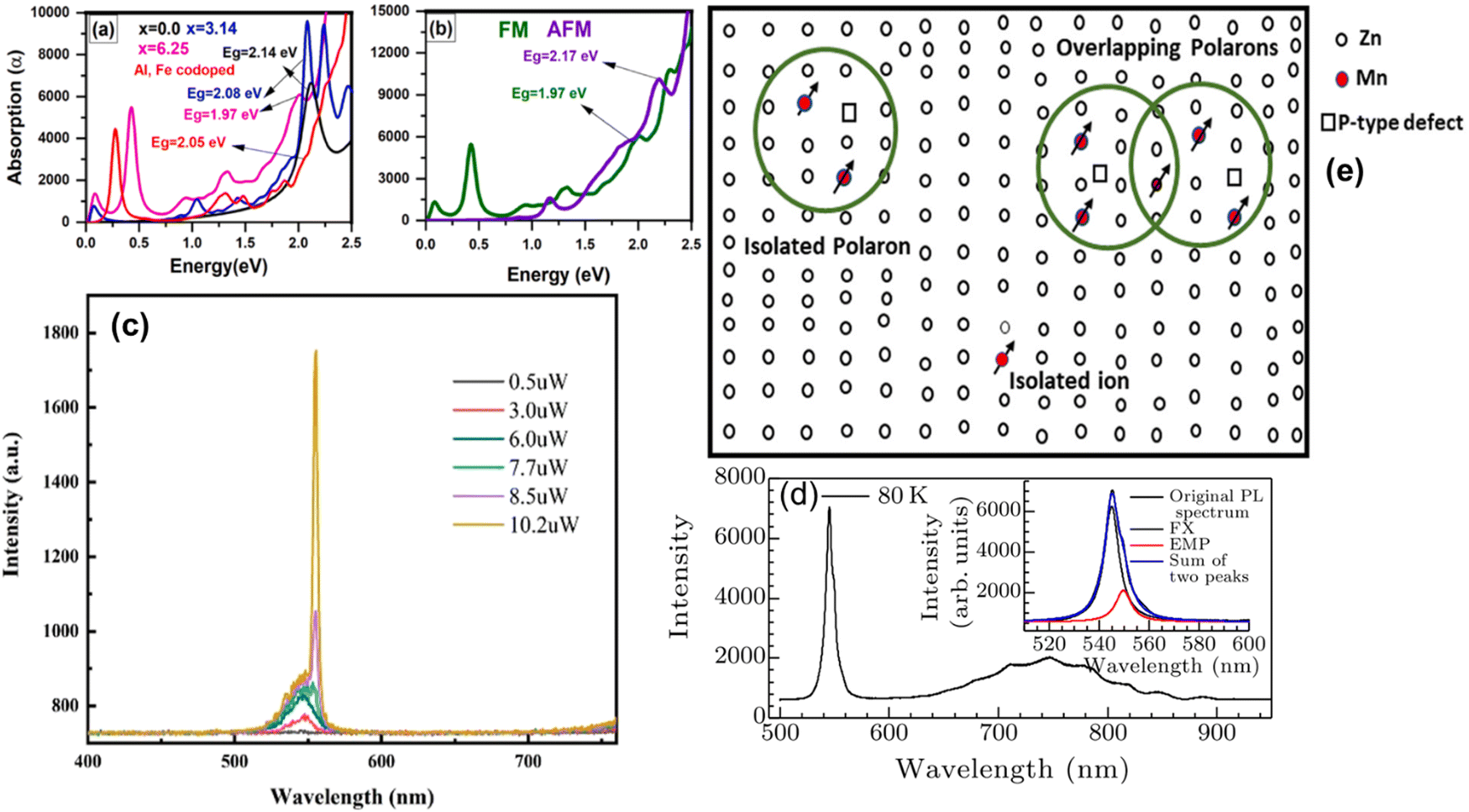 | ||
| Fig. 9 Absorption spectra of (a) single Fe doped, double Fe doped and (Al, Fe) co-doped ZnTe and (b) FM and AFM coupled ion systems. Copyright © 2023, Elsevier.2 (c) PL emission spectra of ZnTe microbelt under femtosecond pulse excitation with a variation in pump power. Copyright © 2023, the American Chemical Society.290 (d) PL spectra of Co-doped ZnTe at 80 K with Lorentz fitting. Copyright © 2018, Chinese Physical Society.289 (e) Schematic diagram of bound magnetic polaron model for Mn(II)-doped ZnTe, Copyright © 2023 Elsevier.1 | ||
Fig. 9a and b show the first-principles calculations study of the magnetic and opto-electronic properties of Fe(II)-doped ZnTe based on the RKKY-exchange. Fe(II) occupies the tetrahedral crystal field, showing a spin-allowed d–d transition in the IR region. The optical bandgap reveals a blue shift due to AFM coupling, whereas the FM coupling results in a redshift in the emission spectrum. The Fe ion in the host lattice has no gain in energy due to the double exchange of the spin states (e2g and t2g) that are fully occupied, supporting the FM interaction. Similarly, the two spin ions of the same spin gain energy due to the super-exchange of half-filled e2g support the AFM interaction. The exchange splitting of the d-state in the FM state is smaller than that in the AFM interaction and the energy gained due to the super-exchange interaction is larger than that due to the double exchange interaction. In the case of the incorporation of an n-type dopant ion in the host lattice, it occupies the spin down partially filled e2g state, which supports the FM configuration. Therefore, the large exchange splitting of the d-state supports that the FM interaction with double exchange is larger than the super-exchange, which favors the FM state in n-type Fe(II)-doped ZnTe. The incorporation of Fe ions in ZnTe and co-doped with Al ions is responsible for the intermediate d-states between the conduction and valence band. The absorption peaks of the Fe ion associated with the intra-band transition appear at 0.2, 0.92 and 1.03 eV, corresponding to the electronic transition of the E2 to T32 and E2 to T32 states, respectively. With an increase in the number of Fe ions, the number of d-states also increases, with the appearance of additional d–d transition peaks due to the Fe–Fe pair system, corresponding to the transition states of E21–E22, E22, E21–E23, E21–T31 and E21–T32 having energies at 0.25, 0.45, 0.88, and 1.31 eV, respectively. The d–d transition intensity increases with an increase in Fe concentration but Al co-doping reduces the d–d transition together with the band-edge transition peaks. Moreover, an increase in the concentration of Fe(II) results in a redshift in the band-edge transition and d–d transition related with the Fe–Fe ion through sp–d exchange coupling. When Al is co-doped in ZnTe, the Fe(II)–Fe(II) ion pair shows a blue shift in its bandgap due to the Burstein–Moss effect. Additionally, in the Fe(II)–Fe(II) ion pair system, the intensity of the absorption coefficients increases with an increase in the Fe concentration, which decreases after co-doping. According to the density of states peaks, the FM and AFM configurations show the occupied and unoccupied d-orbital states for both Fe(II) and Fe(II) co-doped in ZnTe. The d–d intra-band transition exhibits a red and blue shift for the FM and AFM coupled systems, respectively, with different energies showing the influence of the different types of magnetic coupling in the absorption spectra, as confirm by both theoretical and experimental data. The improvement in the opto-electronic and magnetic properties of Fe(II)-doped ZnTe upon n-type (Al) co-doping provides insight into the potential applications of these materials in spin-related photonic and spintronic devices such as photovoltaics and remote sensing.2
Dong et al. showed that the terahertz generation by optical rectification in ZnTe is usually degraded by the following factors: (i) harmonic generation, (ii) two-phonon absorption and (iii) free carrier absorption.294 The inclusion of Te in ZnTe for THz generation was observed by IR transmission spectroscopy. The Te inclusion has a hundreds of picoseconds region and wider width, while that for the ZnTe matrix is several picoseconds. Alternatively, the central frequency and bandwidth of the Te inclusion are 0.1 and 0.6 THz, whereas they are approximately 0.2 and 1.8 THz for ZnTe, respectively. Additionally, the amplitude of the THz waves from the Te inclusion at the center is higher than that from the ZnTe matrix. The Te inclusion in the ZnTe matrix is responsible for the unique emission, which may enhance the multiple reflection of THz pulse. This multiple reflection enhances the phonon polaritons within the host matrix, which is related with the second harmonic generation.294,295 The energy transfer mechanism based on the anti-Stokes emission is beneficial for various technological applications including biological imaging, up-conversion lasers, solar cells and many others.296 Excited state absorption (ESA) showed that the electron transition involves the use of two absorbed photons in intermediate electronic states to create highly excited carriers. Energy transfer induced up-conversion (ETU) is similar to the Auger effect, in which energy transfer occurs from an excited e–h pair to another carrier. Two-photon absorption (TPA) is the simultaneous absorption of two photons in the intermediate state to achieve a high electron transition. The TPA-related emission shows a large anti-Stokes shift without acquiring a real intermediate state at a high excitation density on the nanoscale timescale. Thus, a high density and shorter timescale are key factors in TPA-related linear upconversion absorption. Phonon-assisted anti-Stokes PL (PA-ASPL) only appears where strong electron–phonon interaction occurs at a very low excitation power. The phonon-related anti-Stokes emission involves an indirect optical transition due to the hot exciton effect in polar semiconductors, as discuss above for both ZnTe and CdS nanobelts. Excitons are strongly coupled with optical phonons through deformation potential interaction or Frohlich interaction, which is responsible for the higher order Raman peaks due to resonance phenomena.
Fig. 9e presents a schematic of the BMP model responsible for the ferromagnetism in p-type Mn(II)-doped ZnTe. Different mechanisms, such as double exchange mechanisms, bound magnetic polarons, super-exchange mechanisms, and band-coupling models, have been used to explain the ferromagnetism in DMSs. The most widely considered defect-mediated mechanism for understanding ferromagnetism in dilute magnetic semiconductors is the bound magnetic polaron model. Zn vacancies play a crucial role in understanding the magnetism in Mn(II) in ZnTe, where the 3d states of the Mn ions around the defects couple ferromagnetically to each other, where the hole carriers are bound to form BMPs. The polaron–polaron interaction is ferromagnetically coupled with the carrier–ion–carrier interaction. The paramagnetic (PM) component is attributed to the isolated polarons and Mn(II) ions. In addition, the co-dopant and Zn vacancy boost the room-temperature ferromagnetism. Furthermore, we inferred that the BMP model (defect-mediated model) fit can help understand the origin of ferromagnetism. Our optical study revealed the that Mn(II) doping at the Zn site widens the bandgap of ZnTe and produces spin-forbidden d–d transition peaks on the low energy side of the bandgap. The p-type defects in Mn(II)-doped films produce absorption peaks in the infrared region and improve the absorption efficiency. In addition, the optical bandgap and spin-forbidden d–d transition of Mn(II) to different modes of spin–spin interactions were correlated, and we observed a red shift in the d–d intra-band transition peaks and an optical bandgap in the FM-coupled Mn(II) ion system and a blue shift in the AFM coupled ion system, supporting the experimental observations. The theoretical calculation of Mn(II)-doped ZnTe showed that the occupied spin level of Mn leads to a super-exchange mechanism in p-type semiconductors. The incorporation of Mn leads to ferromagnetism through additional hole carrier formation with the dopant ions. Moreover, the Zn vacancies and co-doped coupled the hole carriers with the spin-up of the Mn(II) ion with stable ferromagnetism behavior. The hybridization of the Te-p level and Mn(II)-d level around the Fermi level supports the stabilized AFM of the d-level due to its full occupation by the spin electron after gaining energy to support the super-exchange mechanism. The double-exchange mechanism appears with no energy gain, which is located just below the conduction band or conduction state minimum. Meanwhile, the overlapping spin-up and spin-down show no magnetism in the AFM coupled ion system. The interaction between two-spin ions with opposite shifts at the d-orbit show the exchange spin splitting of the large AFM state than the FM states. Therefore, the origin of AFM coupling in the ZnTe slab-like structure is due to the super-exchange of electron hopping occurring between the Mn ions via the intermediate p-state of the anion. The experimental results reveal that the hole carriers play a vital role in the ferromagnetism in DMS together with the defect states and co-doping enhances the p-type behavior in semiconductors. In general, the FM state is highly stabilized with additional hole carriers, which are localized at the topmost valence band in ZnTe with broadening due to the symmetry breaking relaxation. Secondly, the Zn vacancy acts as a double acceptor, which generates two holes in the spin-up states by charge transfer in the coupled ion systems. The states split into occupied and empty states in the majority spin channel due to the transfer of charge from the Mn-d state to the defect level of the Zn vacancy. The energy difference is about 135 meV greater than the thermal energy, indicating that the FM state is more stable than AFM above room temperature. The magnetic moment is contributed by the following: (i) Mn(II) ion doped in ZnTe or Mn–Mn interaction, (ii) hybridization between Mn-d and Te-p orbitals with minor magnetic moment and (iii) spin distribution of Mn(II) with Zn vacancy. A large density of spin exists around Mn(II) and the interaction of the Mn ion with the nearest Te atoms is antiferromagnetic. Moreover, the co-doping also enhances the ferromagnetism behavior given that it acts as double acceptor with an energy difference of about 138 meV lower than the AFM state.1
Fig. 9d shows that Co-doped ZnTe exhibits a free exciton emission together with a shoulder peak with the energy difference of 19.4 meV less than the LO phonon at 80 K assigned to the EMP emission. The aggregation of the Co ions results in ferromagnetic spin, which bind with the free excitons to form EMP. Moreover, the broad emission in the range of 600–900 nm corresponds to the d–d transition associated with 4T1(P)→4A2(F) of the ferromagnetic-coupled Co ion in the host lattice from the high d-level of the intra-band transition. Moreover, the power-dependent emission reveals a redshift in the shallow-trapped states (564 nm) due to the generation of a high carrier concentration, which normally appears in low excitonic binding energy semiconductors such as ZnTe (12.6 meV). The high excitation power generates a large number of photoinduced carriers, which are responsible for electron–hole plasma formation on the surface. Secondly, the large radius of the photons and excitons increases the possibility of electron–phonon coupling an increase in electronic scattering, which is responsible for the large red shift at 563 nm. Previous studies deduced the formation and emission of EMP in TM ion-doped II–VI semiconductors, specifying the emission at the long-wave side of FX. A double-peak structure is observed in the range of 540–580 nm and the emission of EMP appears due to the coupling between the free excitons and ferromagnetic spins from the transition metal ions. The emission peak at 572 nm is related with EMP, which corresponds to the phonon and spin interaction. The redshift in the EMP emission indicates that the carrier interaction is dominant and the increase in intensity shows that the strong spin binding effect at a high power is due to the large polaron radius. Therefore, the EMP becomes more dominant even at a high concentration, providing stability to the spin–spin interaction even at room temperature and high excitation power.297
Ni(II) ion doping in ZnTe results in the generation of magnetic polarons together with the hot carrier effect, which can be understand based on power and temperature-dependent PL. The spin–exciton, spin–spin coupling and carrier–phonon interaction emission account for its ferromagnetic properties. The power-dependent luminescence behavior responsible for the hot carrier effect suppresses the charge trapping effect at a low exciton binding energy (8.12 meV). The large polaron radius exhibits the strong interaction between the carrier and magnetic polarons, resulting in an anharmonic effect in which the side-band energy overtones to the LO phonons. The photon-like polariton shows the polarized spin interaction with LO, exhibiting strong spin–phonon polaritons. Multiple emissions show the non-uniform distribution of the Ni ions in the ZnTe nanostructure with a strong exciton emission at the near band edge and lower energy side due to the ferromagnetic coupled Ni pair or cluster interaction with the traps/defect states. The localized spin-induced excitons interact with hole exchange (heavy hole greater than electron) at the topmost valence band in ZnTe to form LEMP. The non-radiative decay of localized spin/excitons is responsible for multiple emissions at room temperature related with photon-like polaritons. The optically polarized anisotropy explains the dielectric contrast due to the degeneracy of the exciton states at the topmost valence band, representing the spin–spin coupling and exciton–spin–phonon and electron–phonon interaction of magnetic polarons of low excitonic binding energy semiconductors for future spin-based optoelectronic devices. The free excitons (FX) interact with the 2LO phonon–spin interaction, corresponding to the 3T1(3F) → 1T1(1G) and EMP peaks with ferromagnetically coupled Ni ions at 3T1(3F) → 1E(1G). In addition, the other d–d transition of single Ni ions (600–900 nm) appears at the low energy side with an energy shift of 14–38 meV due to the localized states. These results demonstrate the spin–spin magnetic coupling and spin–phonon interaction at room temperature, making the new horizon of optically controlled dilute magnetic semiconductor applications more realistic.298
3.2.4.1 Transition metal ion-related luminescence behavior. Fig. 10a shows the power-dependent PL spectra of ZnO:Mn NW prepared via CVD upon excitation by a 355 nm fs laser. At a low pump power, the free exciton peak appears at 3.305 eV with another peak at 3.168 eV ahead of the free exciton peak. The energy difference between the two peaks is about 137 meV, corresponding to the overtone of the A1 2LO mode originating from the polaronic exciton of a bound exciton, which involves spin–phonon coupling. A further increase in excitation power resulted in a superlinear increase in peak B, as shown in Fig. 10a. Also, peak A, which is related with free excitons, slightly increased and decreased swiftly when the power increased from 0.3 to 3 μJ. Fig. 10b and c show the intensity and FWHM as a function of excitation power, respectively. In the high power range, peak B became sharp with a reduction in FWHM. The lasing line of peak B is blue shifted by about 50 cm−1 and analogous to the phase space filling effects of excitons at high excitation, which represents exciton repulsion, not a carrier effect. Above 4.0 μJ, the lasing line narrowed by around 3 meV, which reflects the complete coherent emission with an increase in intensity, as show in Fig. 10b. A further increase in power led to the formation of an additional line in the spectra, corresponding to the dipole–dipole interaction of excitons from the coherent single mode. Fig. 10c shows the single mode lasing of ZnO:Mn NW with the narrow FWHM related with BEC excitons. The low doping profile of ZnO NW showed an emission at a low excitation power due to exciton coupling and electron–phonon coupling at room temperature for the large exciton binding energy (60 meV) semiconductor. Alternatively, a high concentration of Mn ions in the host lattice may weaken the UV emission at low power due to the trapped states within the bandgap. The emission shows the non-linear phonon–phonon coupling in 1D NS with an enhancement in A1 phonons along the axial direction. This strong non-linear coupling may lead to the formation of a 2LO phonon interaction with excitons, exhibiting the boson nature of bipolaron excitons in the 1D system at about 4 μJ cm−2. The increase in intensity and narrow FWHM reflect the coherent two-phonon–exciton formation and condensation, which lead to BEC states at room temperature for ZnO:Mn. The stable BEC in the 1D system is related with the following: (i) coherent and high-density exciton states produced by fs laser, (ii) side crystal face reflection may enhance the high-density exciton, and (iii) the aggregation of free excitons with different orientations assisted by coherent 2LO A1 phonons in the longitudinal direction. Therefore, the high-density bipolaronic exciton emits coherently, reflecting the characteristic of the dynamic BEC statistics. Fig. 10d shows the 3D contour plot of the coherent exciton emission for different laser powers. The emission spectrum of Mn-doped ZnO clearly reveals that the Stokes signal interacts with the LO phonons because electrons interact more strongly with LO phonons rather than other phonons due to the deformation potential interaction.306 In the case of ZnTe, the LO phonon undergoes relative displacement due to its oppositely charged ions, which induce polarization, strongly interacting with electrons through Frohlich interaction.296 Mn-doped ZnO NWs exhibit strong electron–phonon interaction, as observed for the eleven order of LO phonon modes, in which the deformation potential of the dopant ion influences the atom displacement from the equilibrium position. Therefore, the displacement of the atom enhances the lattice polarity and shows multiple phonons due to the strong electron–phonon interaction in Mn-doped ZnO NWs. Secondly, the slight shift towards a higher wavelength is due to the sp–d hybridization between the localized d-electron of the dopant atom and VI-group anion, as observed for other II–VI semiconductors. Thus, magnetic ion doping quenches the band edge emission owing to the radiative absorption by the color center, which highlights the high-order phonon peaks in the hot luminescence process under 325 nm and 355 nm.306
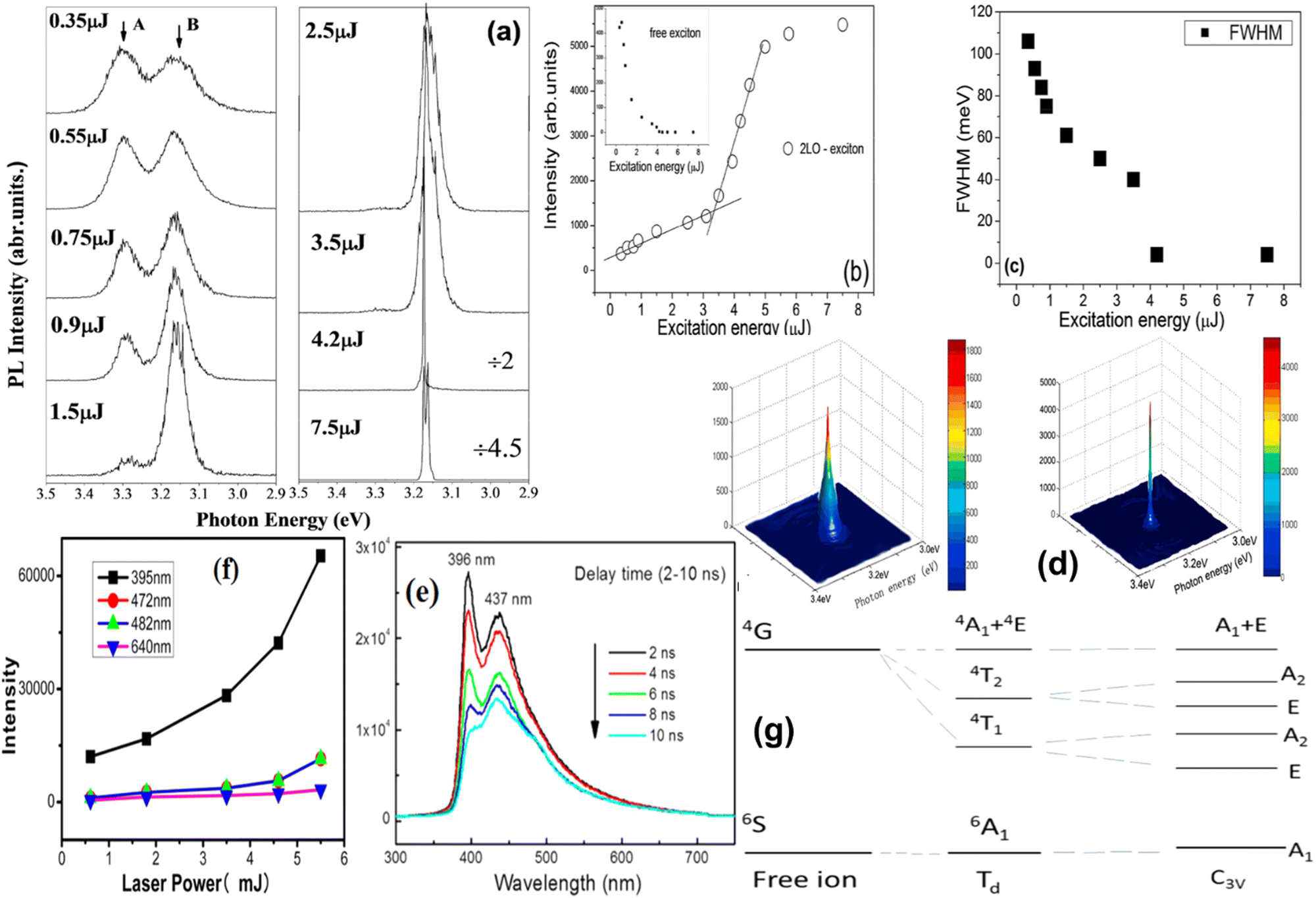 | ||
| Fig. 10 (a) Photoluminescence spectra at various pumping energies of ZnO nanowires. (b) Luminescence intensity vs. laser excitation energy. (c) Luminescence B band FWHM vs. laser excitation energy. (d) Energy profile of the luminescence B line at 3.5 μJ and 4 μJ. Hot luminescence spectra of Mn-doped ZnO NWs, Copyright © 2011, IOP Publishing.307 (e) Time-delayed photoluminescence of ZnO:Mn NW under a laser pulse at 355 nm (duration 2 ns) from the third harmonic of an Nd:YAG laser with the pumping energy of 3.5 mJ. Observed spectral variation after the NW was excited within 2–10 ns delay time range. (f) Dependence of the emission intensity of various wavelengths on the excitation powers. (g) Diagram of Mn(II) levels in ZnO matrix. 6A1 is the ground state and 4T1, 4T2, 4E, and 4A1 are the excited states in ZnO, respectively. Copyright © 2014, the American Chemical Society.4 | ||
TM ion doping in ZnO is important for DMS and their structure and magnetic origin need to be understood. Liu and co-workers explored the magnetic exciton relaxation and spin–spin interaction of Mn-doped ZnO NW prepared via the CVD method.4,308Fig. 10e shows the time-delayed PL of a ZnO:Mn single NW under a laser pulse at 355 nm (duration of 2 ns) from the third harmonic of an Nd:YAG laser with the pumping energy 3.5 mJ. The spectral variation was observed after the NW was excited within a 2–10 ns delay time range. The emissions at 396 nm and 437 nm were observed at a low excitation power, and as the delay time was extended, a shoulder peak appeared at 480 nm together with a shift in the peak at 396 nm to 402 nm. At a high delay time of about 28 ns, the emission peak 472 split into multiple peaks and became sharp under a further delay with the emission of another peak at 636 nm, which is the Mn-related emission. Fig. 10f shows the dependence of the emission intensity of various wavelengths on the excitation powers. According to the results, we conclude that each excitation emission in the luminescence spectrum is time dependent and related to the electronic configuration, carrier–carrier interaction, carrier coupling with spin ion interaction, carrier–phonon interaction and exciton–phonon interaction in the respective host material crystal symmetry.309,310 All the emission peaks observed under different time domains show an increase in the superlinear intensity with laser excitation power, as shown in Fig. 10f. In the case of 1D nanostructures, these phenomena become more interesting, which are specially related to the exciton and exciton–spin relaxation characteristics. Initially, the exciton-related emission in the spectrum exhibits that further recombination with phonons, impurities or magnetic ions occurs, as observed by a fs laser producing free excitons and bipolaron excitons in Mn-doped ZnO NW.307 Moreover, the excitation in ZnO is orientation dependent, as discussed above for vertically aligned and horizontally aligned NW, revealing different quantum efficiencies. Thus, the intermediate states with a lower energy are populated after the relaxation of photoinduced carriers.5,310 The emission at 394 nm for a 2 ns pulse is assigned as the bi-polaron exciton (BPE) or EMP.4,307 According to the schematic diagram (Fig. 10g), the d–d transitions from the 6A1 ground state to the different intermediate 4T1, 4T2, 4E, and 4A1 excited states in ZnO were calculated to be 2.55, 2.85, 2.97, and 2.99 eV, respectively, through CI energy band calculation and photoemission spectra.4,311 Therefore, both the theoretical and experimental correlations provide suitable information about the emission spectra of the ZnO crystal symmetry matrix with and without doping at room temperature. Also, 1D-Mn doped ZnO NWs show coherent emission localized exciton magnetic polarons, which are the source of ferromagnetism in the host matrix to produce coherent EMP emission-related different time domains. This type of 1D single structure is significant for both spintronic- and spin-related photonic devices. The epitaxial growth of a ZnO NW array on sapphire via the chemical vapor transport method and determination of the external quantum efficiency related to the PL of ZnO NW at room temperature have been reported.301,312 Interestingly, the bandgap-related external quantum efficiency (EQE) is strongly dependent on the excitation power density and spot size. In the case of EQE, it is necessary to understand the absorption first, where the band edge emission improves or becomes more intense with an increase in the incident laser power rather than the exciton-related radiative recombination becoming dominant. Alternatively, the defect-related emission becomes more intense than the near band edge, indicating that the non-radiative recombination related with the defect state is dominant in the single structure.
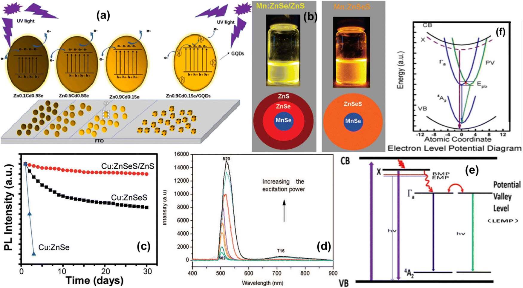 | ||
| Fig. 11 (a) Photoelectron transfer diagram for ZnxCd1−xSe and Zn0.9Cd0.1Se/GQD nanocomposites, Copyright © 2022, Elsevier.314 (b) Digital image of ZnSe/ZnS:Mn (left) and ZnSeS:Mn (right) upon exposure to a UV lamp, Copyright © 2011, ACS publishing.317 (c) The photostability curve plot of Cu:ZnSe, Cu:ZnSeS and Cu:ZnSeS/ZnS d-dots in air and light, Copyright © 2011 The Royal Society of Chemistry.318 (d) PL of 6-fold symmetry branched nanostructures using Ar+ 488 nm as the excitation light source at room temperature, Copyright © 2008, ACS.319 (e) Schematic of recombination dynamics of excitons (X), EMP or BMP near band edge at high excited state to ground state of d–d transition of Co2+ ion (blue color) and STE (green color) within the bandgap of Co(II)-doped ZnSe NR. (f) Electron level potential diagram with atomic coordinates in Co-doped ZnSe NR, Copyright © 2021, IOP publishing.216 | ||
Tang et al. reported the gradient alloy of ZnS/CdxZn1−xSeyS1−y core–shell QDs for liquid crystal displays based on reversible thermal quenching based on the multiphonon process, temporal trap states and re-existing trap states. CdSe provides an effective confinement effect to prevent electron and hole recombination in large band gap materials such as ZnS. Secondly, the core–shell structure confines the wave function of electrons and holes for exciton recombination, which may reduce the generation of interfacial trap defects. Under illumination, the Auger recombination determines the non-radiative recombination at high power. Therefore, the luminescence quenching in QDs is related to the static charge distribution of trap states and surface trap states. Both resonance tunneling and thermally active physical processes followed by radiative recombination with and without tunneling and non-radiative recombination are activated through tunneling.146,171,243,320 ZnCdS and ZnSSe QD alloys show blue emission with a quantum efficiency of 25–50%. In the case of core–shell nanostructures, ZnS can be used as both type-1 and type-II semiconductors with a core of different II–VI semiconductors.21 ZnSSe NRs show spontaneous emission as excited by two-photon pumping with an 800 nm fs pulse laser. An increase in the Se ratio in a single crystal NR resulted in a red shift in its emission from 422 nm to 464 nm. The lasing emission line was achieved at 5.13 mJ cm−2 with a sharp emission intensity (Fig. 12b). A further increase in excitation power resulted in a super-linear emission intensity in a single crystal, which further narrowed the FWHM due to the occurrence of a stimulated emission. A slight blue shift in the emission location corresponds to the phase space-filling effect of excitons at high excitation for low threshold materials such as ZnSSe NR. A two-photon pump with fs laser is a beneficial tool to understand the lasing generated by free excitons and their scattering process in ZnSSe single crystals. The lifetime provides suitable information on the lasing behavior originating from the free excitons or bound excitons in ternary alloys of ZnSe. The amplitude of the decay time of free excitons increases and the bound excitons amplitude decreases above a threshold value due to cavity effects, which saturate the binding states at a high carrier density and reduce the bound exciton amplitudes. The decay time also decreases with an increase in pump energy, which suggests a transition from spontaneous emission to stimulated emission with a narrow bandwidth and super-linear emissive intensity. The different modes illustrate the gain competition and distinct shifts as a function of excitation density.313,321
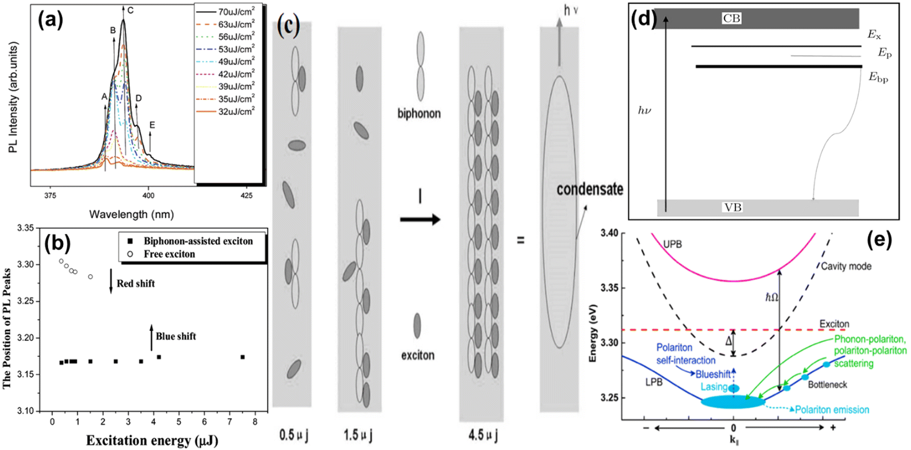 | ||
| Fig. 12 (a) Detailed variation in lasing multi-modes with an increase in the pump fluence in ZnO nanowires. The direction of the arrows shows the increase in pump fluence; the mode marked by arrowhead B appears after A with an increase in pump fluence, and further, the modes marked by arrowheads C, D, and E appear. (b) Photoluminescence peak position from free excitons and 2LO phonon-assisted complex, respectively, showing their dependence on the excitation power, whose magnitude corresponds to the exciton density in the nanowires. Photoluminescence spectra at various pumping energies of ZnO nanowires, Copyright © 2006, ACS Publishing.322 (c) Electronic states and optical processes of ZnO:Mn nanowires. (d) Dependence of peak positions of the photoluminescence from free excitons and 2LO phonon-assisted complex on the excitation energy corresponding to the carrier density in the nanowire, Copyright © 2011, IOP.307 (e) Schematic illustration of the polariton dispersion, polariton relaxation, emission and lasing process. The horizontal dashed line (in red) shows the uncoupled exciton energy and the curve dashed line (in black) shows the uncoupled cavity photon mode. The lines represent the upper polariton branch (UPB, in magenta) and lower polariton branch (LPB, in blue), respectively. ℏΩ is the Rabi splitting energy. Δ is the cavity detuning, Copyright © 2020, Elsevier.323 | ||
Fig. 11d shows the power-dependent PL of ZnS and CdS as 6-fold symmetrical branched NS PL at room temperature. The strong luminescence behavior was observed with a red shift effect ranging from 502 nm to 520 nm, which was assigned to the band-edge dominant recombination of excitons or shallow trapped electron pairs of CdS. Moreover, the bandgap of ZnS and CdZnS is larger than that of CdS; thereby, the CdS-related emission is more prominent in the heterostructure prepared by CVD. The red shift in the spectral behavior is attributed to two factors, as follows: (i) excess carrier formation and (ii) trap state formation due to the presence of nonstoichiometric sites or defects of CdS at the interface. Therefore, a high excitation power is responsible for excess carrier generation due to the nonstoichiometric interface and enhances the carrier–carrier scattering, which may lead to electron–hole plasma formation at a threshold power, resulting in a redshift in the emission. At a low excitation power, the strong emission at 503 nm corresponds to the ZnS/CdS interface because the CdS:Zn layer at the interface may possess a slightly larger bandgap and larger radiative recombination efficiency than individual CdS. As the laser power increases, the amount of photoinduced excitons will increase, which move a longer distance from the interface to CdS ends with a redshift effect and broadening of the emission line. In the case of high power, another peak appeared far from the band-edge at around 673 nm to 800 nm, which was centered at 716 nm.319
3.2.5.1 Transition metal ion-related luminescence behavior. Fig. 11b and c show the luminescence behavior of a ZnSe/ZnS core/shell alloy NC doped with Mn and Cu. The Mn-doped ZnSeS alloyed NC phosphine-free approach resulted in the successful formation of MnSe nanoclusters together with ZnSe/ZnS core/shell (Fig. 11b; left). The formation of small-size nuclei of MnSe required a selenium source at 280 °C, resulting in the formation of MnSe clusters. At the interface of the MnSe core, the ZnSe shell is formed depending on growth temperature of about 260 °C. At 220 °C, the third layer of ZnSe was coated on the doped NC. The PL emission at 584 nm corresponds to the 4T1→6A1 transition of the Mn2+ ion in ZnSe, as discussed earlier.317,324 The slight redshift in absorption indicates that the ZnSe layer grew after each injection of the Zn precursor. The high PL quantum yield was achieved because the Mn ion emission centers were isolated from the surface defects. Further, the ZnS shell grew to form a core/shell nanocrystal, showing a noticeable redshift without alloying between the core/shell with PL emission at 595 nm. The absorption spectra showed a small peak at 400 nm, which is attributed to the excitonic excitation of the host ZnSe/ZnS core/shell NC. Similarly, the alloy formation of ZnSeS showed a blue shift in its spectrum at around 350 nm (Fig. 11b; right). The Mn:ZnSeS alloy showed the Mn-related peak at 605 nm with an increase in the PL quantum yield, indicating a reduction in the interfacial scattering in the alloy shell.317Fig. 11c shows the Cu-doped ZnSe/ZnS core/shell NC and ZnSeS alloy PL quantum yield after 30 days, exhibiting the high stability of the green fluorescent material of Cu-doped NCs. Therefore, the high quantum yield and stability of these NCs make them suitable for various optoelectronic applications such as bioimaging and LEDs. The emission of Cu:ZnSe d-dots was quenched after two days, while that of Cu:ZnSeS NCs decreased slightly but they still exhibited a higher quantum yield than Cu:ZnSe. In contrast, Cu:ZnSeS/ZnS core/shell d-dots exhibited better stability under air and light, maintaining ∼90% of their initial intensity after 30 days. This is because ZnS as the shell protected them from the outer environment and stabilized the Cu emission of the NCs.318 The D states belong to (i) surface defects, (ii) point defects and (iii) impurity defects, while the X state is related to the Co doped in the host matrix (Fig. 11e and f).216 The 1D structure possessed a twin structure (wurtzite and zinc blende), which was formed during VLS growth, as confirmed by the structural analysis, and may be responsible for the D state or the above-mentioned defects.209,313 In the case of the doped nanostructure, the dopant ion is incorporated in a potential valley (green) near the intrinsic atomic potential.224,242,325,326 At room temperature or above room temperature, the potential barrier overlap disappears due to the mixing of the two potential wells, as shown in Fig. 11f. Another reason is the formation of a twinning structure of this state in a potential valley, which removes the energy barrier between the two states.
Similarly, the formation of an Mn-doped ZnSe/ZnS type-I core shell NW alloy through the solution process showed different emissions due to bandgap engineering.21,190,320 Mn doping in ZnSe is another strategy to tune the bandgap in 1D nanostructures and improve the overall luminescence of materials. ZnSe heterostructures formed with small bandgap materials such as CdSe cover a broad emission spectrum and can be employed in various optoelectronics applications. CdZnSe NWs have been prepared via the solution process and physical deposition method by numerous research groups.327–330 A change in the Zn content in the heterostructure causes a blue shift in the energy of the near band-edge and exhibits donor–acceptor pair recombination, corresponding to the presence of Zn vacancies near the valence band or deep acceptor states and shallow states near the conduction band. Moreover, the incorporation of Cd in heterostructures suppresses the zinc vacancies or Zn-defect related emission. Moreover, the adsorption of oxygen or water molecules at the surface of NWs will enhance their photosensitivity due to more surface electrons activating surface resistance. Therefore, the depletion layer on the surface of an n-type semiconductor will extract more electrons than low surface resistance. This capability of heterostructure devices improves the photo-conducting behavior together with switching application. Zn chalcogenide alloys with TM ion doping prepared by the CVD method and solution process can be useful for bandgap tuning by controlling their composition ratio, making Zn chalcogenides very efficient for various optoelectronic applications such as photodetectors, solar cells and LEDs.
4. Application of II–VI nanostructures
Binary and ternary semiconductors of Zn- and Cd-chalcogenides possess remarkable physical and chemical properties and are popular due to their wide range of electronic and optical properties. Most importantly, materials belonging to II–VI semiconductors possess direct band gaps together with high optical absorption and emission coefficients. In addition, binary and ternary II–VI semiconductor alloys are readily miscible, providing a continuous range of properties. Therefore, they can serve as efficient light emitters, such as light diodes, lasers, solar cells, and radiation detectors operating in a wide range from IR to UV and X-ray region. Besides general photovoltaic applications, II–VI semiconductor binary and ternary alloys are also potential candidates for a variety of electronic, electro-optical, sensing, and piezoelectric devices; while few II–VI semiconductors cover the terahertz range. In particular, nanoparticles of II–VI semiconductors, such as QDs, 1D structures, and core–shell structures, can be used for the development of gas sensors, electrochemical sensors, and biosensors. As the device scales down to the few nanometer range, their tunable bandgap, high extinction coefficient, possible multiple exciton generation, and unique electronic and transport properties make them highly attractive in the research community. Therefore, the preparation methodology, doping concentration and crystalline quality of this class of II–VI semiconductors make them more important that III–V and other semiconductors. Currently, the blending of II–VI semiconductors with perovskites has been performed to form a new class of hybrid devices, achieving high sensing, opto-electronics and bio-medical device applications. In addition to the device-centric research, herein we also discuss the potential applications of II–VI semiconductor nanostructures in fields such as sensing, imaging, and quantum information processing. Thus, these applications can be further explored in future studies, investigating new sensing modalities, enhancing the sensitivity, or integrating these materials into advanced imaging systems with improved resolution and sensitivity. Moreover, our research underscores the significance of understanding the fundamental properties and phenomena in materials, such as carrier dynamics, spin-related effects, and optical properties in II–VI semiconductor nanostructures. Future studies can focus on unraveling these intricate mechanisms to pave the way for tailored material design and enhanced device functionalities.331–3344.1 Photonic and optoelectronic applications
1D nanostructures have diverse potential applications, especially in photonics and optoelectronics due to their excellent optical properties. 1D nanostructures of II–VI semiconductors have been employed in a wide range of photonic applications such as tunable lasers, leading to white light generation, photonic integrated circuits and many sensing applications. This section highlights some of the interesting instances of the application of binary and ternary alloys and TM ion-doped II–VI semiconductor matrix in detail.Fig. 12a shows that heavily Mn-doped ZnO shows different modes in its luminescence spectrum under different excitation powers. With an increase in the pump power, the carrier interaction became stronger with a redshift due to the amplified spontaneous emission. A high excitation power may lead to electron–hole plasma formation, which increases the carrier interaction in a specific direction to support the lasing mode simultaneously. In comparison with the low doping profile (Fig. 10), the free exciton emission is suppressed by the strong scattering of the impurity ions and phonons. At a low pump excitation, the stimulated emission is due to the exciton–exciton interaction. A further increase in power resulted in an increase in the emission intensity, reflecting the giant oscillator strength and cooperative radiation of localized excitons. At a high power excitation, electron–hole plasma formation becomes dominant, which results in a redshift in emission with multimode lasing for a high Mn concentration. Fig. 12b shows the low Mn doping profile in ZnO at different fs laser excitation at room temperature, as discussed in Fig. 10 (peaks A and B). The blue shift in the emission is due to the phase space filling effect without carrier scattering of excitons at high power. At 4.2 μJ, the coherent transition of the bipolaronic state enhances the intensity and narrows the FWHM of the emission spectrum. With a further increase in pump power (7.5 μJ), the peak energy width became 10.5 meV (second peak appears in the emission spectrum), which is assigned to the dipole–dipole interaction of different coherent states. According to the experimental results, the emission behavior is similar for the low and high doping profiles at a high excitation with a change in the threshold power, which is dependent on the doping profile. Secondly, the redshift in peak A is attributed to the aggregation of neighboring excitons or screening to enhance the Coulomb interaction between free carriers through bandgap renormalization.
Liu et al. revealed that the lasing behavior in Mn-doped ZnO is due to the condensation of magnetic polaronic excitons in 1D NWs prepared by the VLS mechanism.307 To understand the condensation of polaronic excitons, it is necessary to understand all the possible transition states in the host material. At a low excitation power, the exciton and exciton–phonon related peak becomes prominent in the spectrum, whereas at high excitation power, the exciton–phonon interaction is dominant and generates polaronic excitons (bound exciton). The lasing phenomenon in Mn-doped ZnO is owing to the bound excitons, similar to the emission of Bose–Einstein condensation (BEC) excitons, as shown in Fig. 12c. Fig. 12d shows the change in the electronic properties of ZnO with the incorporation of dopant ions. A low doping profile results in strong electron–phonon interactions due to the 2LO of the A1 mode coupled with excitons. FM coupling with coherent excitons result in magnetic polaronic exciton interaction, which condensates by a fs laser to realize the BEC in real confined space. Another key factor related to lasing is Mn doping in the host crystal. A high doping concentration has a higher lasing threshold value than the low doping samples. Therefore, free excitons, coupled spins and bi-phonons lead to the formation of exciton magnetic polarons and condensation-related emissions, which are a function of the doping concentration and pump power for ZnO:Mn lasing; thereby, the intra- and inter-band transitions need to be understood to determine the shift in the emission spectrum under different conditions. The phonon–exciton complex has a higher binding energy than free excitons and two-phonon mode, and therefore both the free exciton- and bi-phonon-related emissions appear at a low excitation pump power owing to their high thermal stability at room temperature. BEC exists in ZnO:Mn-doped nanostructures due to the following reasons: (i) free excitons transform efficiently into bi-polaronic excitons, (ii) NW side reflection may confine the high excitons, which reduces the diffusion or expansion effect and (iii) the aggregation of free excitons with the coherent 2LO A1 mode at a high density. In the case of 1D nanostructures, their crystal orientation is also an important factor that can lead to a reduction in the exciton energy in their interaction and limit the bi-phonon-related emission. In the parallel orientation, the dipole repulsion increases the exciton energy, which exhibits a redshift at a low excitation pump power. Meanwhile, coupled excitons aggregate and the related repulsion increases in the parallel orientation, which will enhance the bipolaronic excitons at high density and characteristic of dynamic BEC emitting light coherently without other available states.5
Optical characterization tools such as PL provide suitable exciton information under different powers. In the case of a low Mn concentration, the free excitons are depleted by the coupling of LO phonons and ion spins at high power, leading to the formation of EMP with a large exciton binding energy and strong electron–phonon coupling semiconductors such as ZnO. Strong exciton–phonon coupling materials normally exhibit an increase in LO mode phonons with the addition of impurity ions. Thus, the LO phonon mode coupled with bound excitons results in the polariton–exciton emission. Mn:ZnO exhibits the EMP corresponding to the 2LO-exciton state at a low excitation energy due to multiphonon exciton but the 3LO and LO coupled exciton emission band is not coupled with free excitons. EMP attain higher thermal stability due to their higher exciton binding energy than thermal energy (26 meV). High exciton binding energy semiconductors possess higher stability of exciton–phonon coupling and exciton–spin interaction at room temperature. A high doping concentration enhances the exciton–phonon coupling and increases the trapped states together with the bandgap. Under these conditions, the emission spectra reflect the forbidden selection rule for one-phonon transition and allow a two-phonon transition or facilitate the bi-polaron process, leading to non-linear interaction in 1D structures. Therefore, the bosonic phonon and exciton dominant the coherent excitonic state of the bound exciton in polar semiconductors, dominating the EMP emission. The EMP peak shows a rapid enhancement, narrowing FWHM and slight blue shift depending on the power due to the exciton–exciton interaction and coherent two-phonon–exciton coupled with spin. Bi-polaron exciton transformation in 1D nanostructures is produced by temporal, coherent and high-density excitons upon excitation by fs laser. High-density excitons in 1D nanostructures are dependent on their crystal face reflection or aggregation of free-excitons, exhibiting coherency in a specific orientation or crystal direction. In the case of the wurtzite structure, the polarization of light–matter interaction shows the orientation-dependent exciton emission due to a change in the dipole force along the parallel or perpendicular direction. In spin-dependent semiconductors, the FM spin exchange coupling in a magnetic field changes the dipole force and aggregation of excitons or spin ions responsible for EMP formation in 1D nanostructures. Therefore, bi-polaronic excitons aggregated in a high density emit coherent light, which resembles a characteristic of the dynamic exciton BEC state (similar to Cooper pairs in a superconductor) in a semiconductor 1D NW structure. Recently, Zou et al. explained the identification of coupled spins in 1D NWs and its origin. According to the magnetic measurement, the origin of the FM coupled with spin inside the host lattice was doubtful. However, the ns time-delay PL spectra show PL relaxation due to the local d–d transition. The strong electron–phonon coupling and spin ion in the host lattice indicate FM coupling in the polariton–exciton emission with the energy position, indicating the origin of the ferromagnetism in DMS. Moreover, the NW cavity demonstrates exciton decay into a very narrow mode of coupling, which is strong enough to produce polariton lasing and polariton condensation in 1D nanostructures. This long-range elementary excitation has spin-polarized character and can give collective EMP condensate at a high density. In QDs, EMP can be easily formed, but without long-range LO phonon coupling, as observed by the difference in PL behaviors. PL can be employed to identify the spin ion FM coupled aggregate d–d transition in 1D structures with a slight redshift with its FM spin cluster. This type of cluster in 1D nano/micrometer sized structures favors EMP formation and enables strong single-mode lasing from the BEC-like state of collective EMPs in the DMS structure.5 Zhao et al. achieved low threshold lasing in a thin 1D pure ZnO NW WGM at room temperature through surface plasmon promoted by single-mode polaritons.323Fig. 12e shows a schematic diagram of polariton dispersion for lasing, corresponding to the relaxation and emission of coherent plasmon–polariton in cavity-mode ZnO. The horizontal dashed line (in red) shows the uncoupled energy (exciton energy) and the curve dashed line (in black) shows the uncoupled cavity photon mode. The upper polariton branch (UPB, in magenta) and lower polariton branch (LPB, in blue) show the Rabi splitting energy (ℏΩ) and cavity detuning (Δ), respectively. A nano-laser of ZnO NW on graphene–insulator–metal platform exhibited gate-modulated lasing based on the sensitivity of surface plasmon polaritons to the cavity effect. The electric field distribution on integrated circuits on the nanoscale has potential application as a function of gate voltage. Under an applied voltage, the electric field is shifted away from the metal surface, which results in the internal loss of lasing. Therefore, a high-applied voltage modulates the low lasing threshold and vice versa. The PL-related peak intensities were recorded in a repeatability test over five periods, where VG was set as 6V and 0 V in the on-state and off-state, respectively, and the switching period was 1 s. In each positive cycle of 6 V, the on-state accumulated surface electrons on the metal surface, which may increase the plasma frequency at the metal side, resulting in the internal loss of the surface plasmon polariton mode at a fixed pumping power. Therefore, the lasing signal could be dynamically modulated by gate switching.343
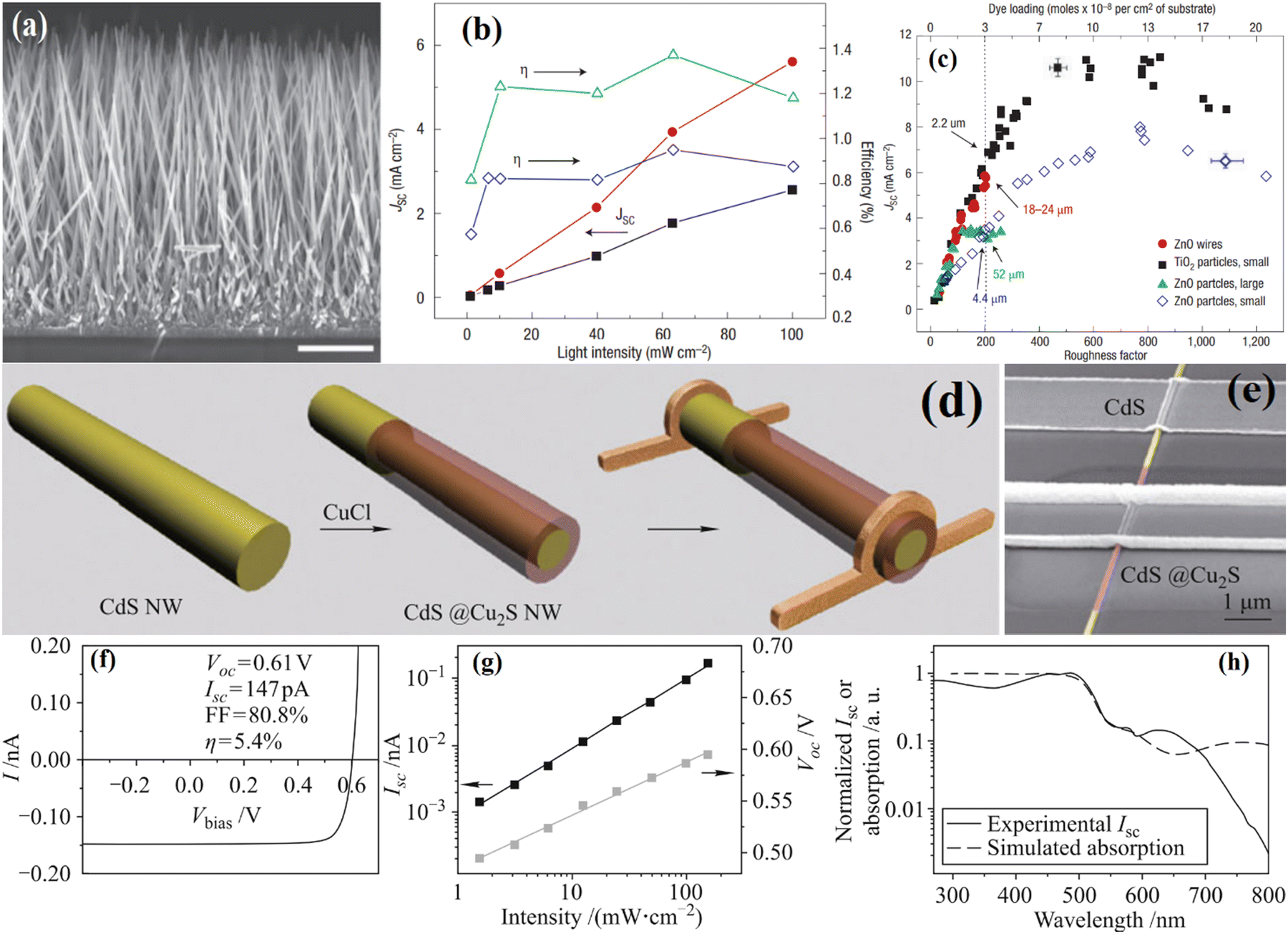 | ||
| Fig. 13 (a) Scanning electron microscopy cross-section image of ZnO nanowire array on FTO for dye-sensitized cell. The wires are in direct contact with the substrate, with no intervening particle layer. (b) Short-circuit current density and efficiency as a function of light intensity for cells with roughness factors ranging from 75 to 200. Each of the four parameters is represented by data from two different devices to provide an estimate of the range of their variability. Active cell size: 0.8 cm2. (c) Short-circuit current density versus roughness factor for cells based on ZnO wires, small TiO2 particles, and large and small ZnO particles, Copyright © 2005, Nature.345 (d) Schematic diagram of core-shell CdS/Cu2S single NW. (e) SEM image of a single NW. (f) I–V curve of a single-NW under 1 sun (AM 1.5 G) irradiation. (g) Variation in Isc and Voc with light intensity. (h) Wavelength dependence of photocurrent compared with simulated absorption, Copyright © 2011, Nature.55 | ||
Tang et al. reported that a single CdS NW showed a better response than planar devices.55 The high-crystalline single CdS radial NW p–n junction exhibited an open circuit voltage of 0.6 V and fill factor of 80%, as shown in Fig. 13f. The CdS/Cu2S core–shell NWs showed higher values than the planar devices at a low open circuit voltage with a reduced light intensity (Fig. 13d and e). The interfacial junction between core–shell materials should be high quality and the VLS mechanism should provide a high-crystalline interface between CdS/Cu2S, with the calculated overall efficiency of 5.6% with a lower current density (Fig. 13g and h). Moreover, the solar cell efficiency is also dependent on the thickness of the shell materials, where an increase in the shell thickness leads to absorption within the interface, affecting the efficiencies of radial solar cells. Additionally, horizontal devices can facilitate the study of the uniformity of charge collection as a function of orientation and single NW. For this purpose, the scanning photocurrent mapping (SPCM) of horizontal NW demonstrated that the core–shell region is more active for charge separation, while the edge exhibits a sharp drop-off. The radial p–n junction has benefits of charge collection from CdS, which suffers from a low minority diffusion length. Moreover, multiple devices with parallel and series configurations based on core–shell single NW provide a flexible absorption range at low cost and better photonic device performance than planar devices. CdS/CdO core shell and other ternary II–VI nanostructures are potential materials for future photonic applications.75,174
 | ||
| Fig. 14 (a) Dark current and (b) photo-current at various humidity levels under different bias and the inset shows the IV characteristics in the dark (a) and light (b) at different relative humidity. (c) Relative humidity-dependent moisture responsivity of the sensor in dark and bright fields, respectively. (d) Resistance at various relative humidity of the sensor in dark and bright fields, respectively. (e) Schematic theoretical diagram of humidity sensing by the sensor.188 | ||
Recently, many groups have devoted their efforts to fabricating flexible photodetectors based on 1D and 2D structures. In the case of II–VI 1D nanostructures, there are many reports on both ZnO and CdS related to their photo-detection properties, which depend on the following: (i) composition gradient, (ii) incorporation of dopant and (iii) synthetic mechanism. 1D CdS NW and WSe2 2D flakes were used as the substrate for the fabrication of a photodetector by Lin and co-workers.347 Both Lin and Du highlighted the importance of van der Waals heterostructure growth.347,349 The Xiong group reported the growth of various II–VI semiconductor nanostructures, reporting van der Waals epitaxial growth by the VLS mechanism extensively.10 Their photo-response as a function of time and illumination intensity were investigated. With an increase in the illumination intensity, the photo-response of the device decreased due to the interface trap states. The I–t characteristic curve showed the stability of the photodetector under different illumination intensities at a fixed bias condition of VD = +2 V. Also, it was shown that its response time is less than 1 s and its switching behavior was retained after multiple cycle tests under strain. Similarly, the I–V characteristic curves under light and without light for the flexible photodetector under different strains were recorded together with the effect of different strain on the output characteristic curve of the photodetector. According to the results, the current of the CdS NW increased under illumination but strain had no impact on the performance of the device. Lou et al. also fabricated a 1D ZnO–SnO2 photodetector for UV photodetection on a PI substrate.350 The ZnO–SnO2 devices showed excellent UV photodetection under ambient condition. The conductivity of both materials improved due to the oxygen on their surface enhancing the carrier response, which may improve the high ION–IOFF ratio, fast response time and good reversibility.350 Moreover, Yang et al. reported that a ZnO NW covers a broad range of the spectrum for detection under different laser excitation and exhibits ultrahigh sensitivity, fast response speed and good flexibility for future optoelectronic circuits, switches, etc.60,301,351 Guo et al. synthesized highly crystalline tin-doped CdS NW for tunable optical loss and multi-band photodetection using the CVD method.96,173,188 CdS NWs showed pump power-dependent propagation loss of the near band edge emission and defect-related emission. According to the low temperature PL measurement, the activation energy was calculated to be 34.29 meV, illustrating carrier decay owing to exciton recombination. The high photo-response (51.2 A W−1), high gain (313.3) and stable optical switching at VDS = 3 V revealed the importance of 1D II–VI semiconductors in the design of integrated optical interconnection chips.96 Lieber et al. employed CdS NW on silicon to produce a nanoscale injection laser to cover a wide range of the spectrum, and also integrated it as a single or multiple color laser in silicon microelectronics and single wire on-chip devices.40,352–354 CdS single NWs have a high injection rate due to cavity formation and some issues can also be addressed by axial composition, core–shell heterostructure, composition gradient and TM ion doping or metal doping on the surface of 1D nanostructures. Moreover, the radial p–n junction of n-CdS and p-Si NW for an avalanche photodiode demonstrated ultrahigh sensitivity with detection limits of less than 100 photons for ultra-dense integrated systems, sensing and imaging applications.353
 | ||
| Fig. 15 (a) Waveguide demonstration of CdSxSe1−x nanoribbons. Copyright © 2007, the American Chemical Society. (b) Selective waveguide from the branched architecture of the CdSxSe1−x nanostructures and (c) PL spectra of the marked locations in (b), Copyright © 2012, the American Chemical Society.78 (d) Characterization of optical wave guiding in straight and bent nanowires. (top) Schematic diagram. (2nd) Scanning optical microscopy (SOM) image illustrating the focused laser spot scanned over the sample, while monitoring light emission from one end of the nanowire. (3rd) SEM image of a single CdS nanowire and (4th) corresponding SOM image. (5th) SEM image of a single kink CdS nanowire and (last) corresponding SOM image at different positions (marked 1 and 2), Copyright © 2004, the American Chemical Society.352 | ||
Due to its wide bandgap with cylinder geometry or hexagonal structure with large dielectric constant, Sn doping in CdS show good waveguide behavior, which was activated as a superlattice 1D nano/micro-wire, as shown in Fig. 16a. The inset shows an optical micrograph of the Sn-doped CdS. Its optical behavior was similar to a 1D photonic crystal (PC). Fig. 16b shows a schematic diagram of the CdS/CdS:SnS2 junction within the single wire-like structure. The CdS segment in the superlattice wire confines the transport of photons, while due to the large refractive index of SnS2, it acts as a reflector to trap light within its optical micro-cavities. Periodic bright emission arises from the interference of the coherently scattered light wave within the coupled cavities not related with the Fabry–Perot mode (Fig. 16c–h).194 The different emission modes with a variation in wavelength can be imaged with this 1D PC, behaving like a local photon bunch. Each mode comes from the neighboring two cavities and can propagate at a very long distance. The macroscopic mode number can follow the Bloch oscillation character in a broad emission range, indicating a strong nonlinear photonic structure for exciton–photon interactions. Moreover, the incorporation of Sn(IV) in the CdS lattice results in a bandgap edge and trap state emission due to the nonlinear electron–phonon coupling or anharmonicity effect. The exciton trapped by local impurity states is related to paired states or the deep trapped states involve different recombination rates of relaxation, as shown in Fig. 16i.194,196,359 Similar behavior of color-tunable period spatial emission was observed in ZnO/FeZn2O4 and CdS1−xSex/Sn:CdS1−xSex superlattice by varying the composition gradient from 0 to 0.4.96,196,360–362 The light transports along the axis and is periodically emitted at the adjacent joint segment. A change in the refractive index of CdSSe and Sn forms the neighboring alloy segment, which acts as a microcavity through the reflection interface, where light partially leaks through the joints. The periodic bright emissions arise from the interference of coherently oscillated light within the coupled microcavities, producing multi-peaks at the low energy side. The strong absorption above the bandgap cannot transport far within the wire, and thus it cannot produce waveguide modes. Fig. 16i shows that PL spectrum exhibits a strong band edge emission at ∼551 nm and several accompanying shoulders related to the coupled cavity modes. The mapping profile in the wavelength range of 606–626 nm is shown in Fig. 16h. The photonic modulation and possible exciton coherent emission are combined in different optical microcavities. Thus, we can conclude that these emission contours were produced by the combined contributions of the coupled optical microcavity modes and local excitons within this 1D photonic crystal wire.362
 | ||
| Fig. 16 Far-field PL images of an excited sample with different reaction times: (a) 20 min and (b) 30 min. Insets in (a) and (b) are the corresponding optical images. (c) Schematic representation of the emission process in the 1D superlattice wire, Copyright © 2010, the American Chemical Society.194 (d) Schematic diagram of the branched nanostructure of 355 nm incident laser (inset is the optical microscope image). (e)–(g) Real-color dark-field photographs under the illumination of a 355 nm laser with an increase in pumping power density, with a scale bar of 20 μm, Copyright © 2012, Wiley-VCH. (h) The photoluminescence mapping of CdS:Sn microwire shows photonic modulation in multipeak range.194 | ||
Branched-like nanostructures have been extensively used for various applications, as suggested by the Lieber and Yang group. Liu et al. also fabricated a nanoscale laser array of branched-like structures of CdS doped with Sn, as shown in Fig. 17a–d. Sn acts as a junction, which splits into a multichannel nanostructure, resulting in effective light confinement and oscillation. Under excitation, a strong band-edge emission was observed and Sn reflected the light scattered from the branch segment. Thus, the oscillation of light within the branch and trunks shows the multi-point lasing high-quality factor of up to 990 with a low threshold. The waveguide performance of the hierarchical trunk-branch CdS NW array excited by UV light showed bright green emission that propagates along the branch and emits from the tips, as shown in Fig. 17b. As the central part is excited, the light propagating from the tips of the branches is stronger than the trunk-branch (Fig. 17b) due to the propagation distance, as shown in Fig. 17c. As can be seen in Fig. 17b and c, the branch-like structure shows a waveguide nature and its propagating distance shows marginal damping in emission. The excited trunk shows efficient light coupled between the trunk and branches in a monolithic structure, as shown in Fig. 17d. This exceptional optical coupling motivates optical integrated device applications such as active waveguide trunk−branch cavities for 1D NWs to hundreds of branch wires.89,96,100,359,363
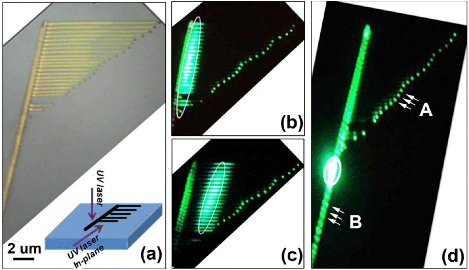 | ||
| Fig. 17 (a) Optical microscopy image of the yellowish CdS comb structure on an Si wafer. The inset schematically shows the different illumination directions and areas of the UV laser (GaN laser diode at 405 nm wavelength). (b) Green photoluminescence with lateral (in-plane) illumination collimated at the trunk–branch junctions, (c) at the central part of the branches, and (d) vertically collimated as indicated by the white ellipses. Note that the arrows marked by B indicate the periodic emission of light resulting from the Fabry–Perot cavity for lasing; the arrows marked by A indicate the light emission from the end-tip of the branches, Copyright © 2013, ACS Publications.89 | ||
The electroluminescence (EL) of CdSe/ZnS QD (QLED) and multilayer micro cavity-based QD (MQLED) was used to study the performance of green and blue LEDs (Fig. 18b and c). The CIF diagram of MQLED shows the efficiency achieved for different colors for RBG (Fig. 18a). The significantly improved optoelectronic performances of MQLEDs demonstrate that the optimization of optical properties plays the same important role in determining the EL performance as that of electrical properties. Meanwhile, the microcavity structure can be applied in low-threshold lasers, cavity quantum electrodynamics, biological detection, and high-performance filters. A further improvement in its Q value can lead to an extremely narrow FWHM and a low-loss optical resonator, which indicates that a high Q microcavity is a promising and practical structure for achieving electrically pumped QD lasers.372 QDs as a display medium for holographic 3D applications with hydrogel composites exhibit very attractive properties such as high transparency, highly saturated color, fast response, low cost, simple process and scalable and healable characteristics. According to the results, the fabricated PVA hydrogels with different QDs are potential smart display mediums for colorful, real-time 3D displays and have potential in other intelligent optical devices.373
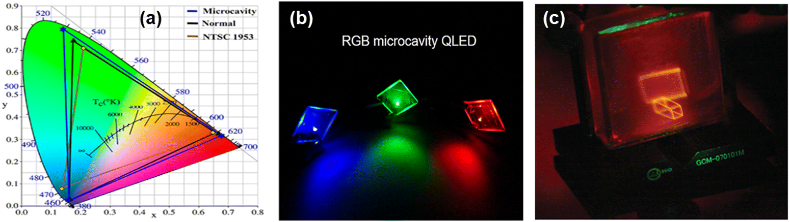
4.2 Electronic and sensing applications
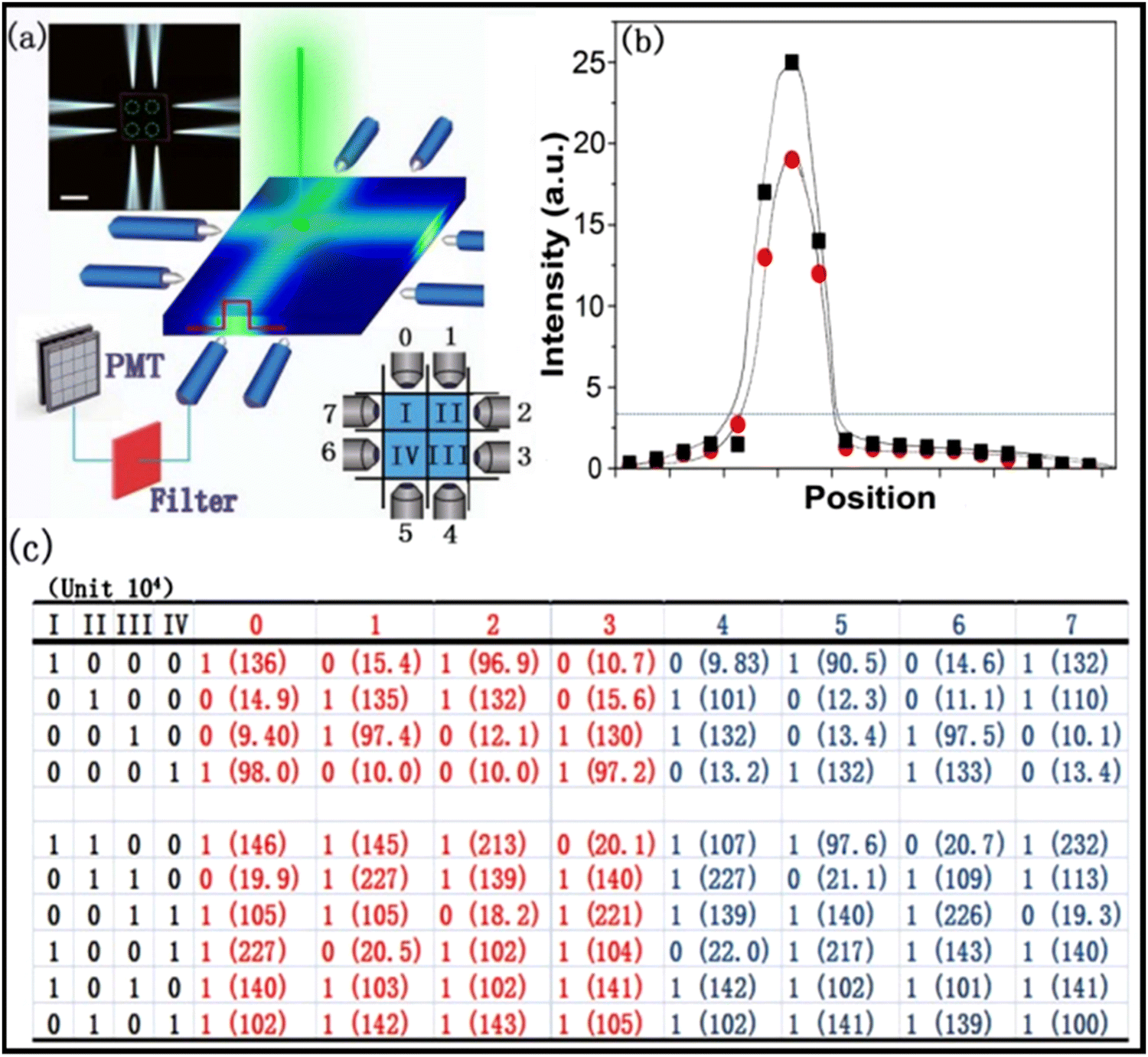 | ||
| Fig. 19 (a) Schematic diagram of a real-intensity measurement system with the fiber tips together with a photomultiplier tube as the detector unit based on a square nanoplate (dark blue). Top inset: Real dark-field image of a square nanoplate with a size of 25 × 25 μm. The fiber tips with a diameter of 250 nm were arranged around the nanoplate. Scale bar is 10 μm. Bottom right inset: Simple schematic of the top view of the whole microsystem. (b) Lighting position-dependent intensity change along the top edge (black square) and right side edge (red circle) clockwise, respectively. The x-axis represents the scanning position. The line corresponds to the threshold-intensity level. (c) Detailed state of each fiber together with the excitation position. The first four columns represent different excitation positions of (1000) for region I, (0100) for region II, and so on. The columns with numbers from 0 to 7 represent the actual emitting-out states at eight different edge positions corresponding to the different excitation regions. In each table unit, the real emission intensity is given in brackets, Copyright © 2017, IOP Publishing.383 | ||
4.2.2.1 FET sensors. Similar to planar FETs, nanoFETs can be controlled by applying an electric potential to control the conduction in their channels, making nano-FETs ideal candidates for chemical and biological sensing.374 For example, in p-type Si NW, the receptor (chemical/bio-molecule) binding of molecules with negative charges leads to the formation of an accumulation layer in its channel, resulting in an increase in conductance. However, binding of molecules with positive charges will deplete the holes in the active layer, which will reduce the conductance. Thus, NW FETs produce real-time directional electrical information on biological events related to binding/unbinding, enzymatic reactions, and electron transfer, with superior capabilities for emerging platforms to investigate biological samples. Also, the SiO2 layer on the surface of Si NW is nontoxic and can sense the hydrogen in lipid bilayers with and without ligand-gating, amino groups and silanol groups (Si−OH). Silicon NWs have been extensively used owing to the fact that they are mature materials in comparison with other II–VI materials and widely used for bio-molecular sensing. However, ZnO NWs have also been used for the development of FET biosensors.351,386
4.2.2.2 Protein sensors. The sensitive detection of proteins related to disease markers offers substantial potential for the diagnosis and treatment of diseases, where real-time protein sensing was first demonstrated in 2001. Nano FETs have the capability to sense biotin receptors, detect streptavidin (concentration down to 10 pM), biotin-monoclonal anti-biotin binding and calmodulin in real time. In a recent study, a basic approach was used to demonstrate the successful concentration-dependent detection of cardiac troponin T390, SARS virus nucleocapsid proteins, and bovine serum albumin together with genomics and proteomics for diagnosing complex diseases such as cancers. Moreover, the availability of altered biomarkers matched with different phases of diseases can help in their initial detection and robust diagnosis.18,28,387
4.2.2.3 Nucleic acid detection. A major difference between nucleic acid and protein detection is the high density of negative charges on the nucleic acid phosphate, which increases the high ionic strength barriers to screen the repulsion in the active channel region and allow binding when DNA or RNA is used as the probe molecule. However, high ionic strength solutions have a short Debye screening length, which can make detection difficult. Therefore, solutions that have a high ionic strength binding/screening require the use of neutral charge peptide nucleic acids (PNAs), which exhibit excellent binding affinity with DNA at lower ionic strengths. Si NWs with PNA probe molecules exhibit time-dependent conductance changes depending on the selective binding of the complementary target DNA at low concentrations (10 fM). In addition to sensing protein binding/unbinding, the real-time detection of nucleic acids (e.g., DNAs and RNAs) has been successfully carried out using Si and GaN NW FET devices.387,388 Multi-segment CdTe–Au–CdTe NWs were used in devices in which the Au segments were modified with thiol-terminated DNA probes, where binding to these probes induced a conductance change in the overall device structure.389,390
4.2.2.4 Virus detection. Viruses are the main origin of infectious diseases, which continue to be the main cause of death globally. In this case, the successful treatment of viral diseases often depends on the quick and precise identification of viruses at ultralow concentrations in living organisms. An Si NW-based nanoFET-based was successfully employed to detect the Influenza A virus for the first time. By recording the analogous electrical conductance fluctuations upon binding/unbinding of the virus particles to monoclonal-antibody-modified Si NWs, the selective detection of Influenza A at the single-particle level was successfully demonstrated. Another example of virus detection is the identification of dengue. A specific nucleic acid fragment with 69 base pairs derived from the dengue serotype 2 virus genome sequence was selected as the target DNA and amplified by the reverse transcription polymerase chain reaction (RT-PCR). The hybridization of the target DNA- and PNA-functionalized Si NW FET sensors increased the device resistance, leading to a sensitivity limit down to 10 fM.18,29,389,391
4.3 Spintronics
Spintronic-based devices open a new chapter in electronic devices scaled down on a single chip to follow Moore's law, which are controlled by the spin degree of freedom of charge carriers. The realization of these devices in 1925 was enabled by the continuous optimization of the nature of TM ions in various semiconductors. However, there is still room for improvement to explore their fascinating functionality for various electronic applications especially 1D systems. The unique optical response of low-dimensional and spin-controlled behavior opens new horizons in spintronic devices based on spin-dependent electronic properties of FM behavior.392 The incorporation of TM ions in II–VI semiconductors results in spin splitting of their conduction and valence bands through the exchange coupling of sp–d between the delocalized carriers and core spin. Wide bandgap semiconductors such as GaN and ZnO also exhibit the spin–carrier interaction above room temperature. Ternary alloy formation or heterojunction devices can be frequently used for spin-dependent transport across the interface between different materials. Mn ions introduce spins and holes in the valence band in GaAs, point defects in SnTe and MnTe, and shallow acceptor impurities in CdMnTe and ZnMnTe, where the polarized electrons permit the injection of spins in normal semiconductors. The FM order of spin ions is mediated by the carriers in Mn-based DMS in II–VI semiconductors. The spin–spin interaction becomes dominant in the presence of the divalent Mn ion through hybridization between the anion and d-states of the TM ion. The super-exchange of the divalent TM ion may lead to the formation of AFM coupling.393,394 The spin–carrier interaction in n-type and p-type semiconductors is related to the spin-polarized electrons or holes in DMS. The spin polarization of injected carriers can be detected by circular polarized light, also known as spin LEDs. However, the spin relaxation time for holes is much shorter than that for electrons in QW based spin-LEDs. Moreover, neuromorphic computing uses brain-inspired principles to design circuits that can perform computational tasks with superior power efficiency based on spintronic nano-devices, in which electronic devices create artificial neurons and synapses with efficient energy integrated circuits. Spintronic-based neuromorphic computing can effectively perform pattern recognition in associative memory.395At a low temperature (5 K), CdTe/ZnTe QDs doped with Cr ions show spin relaxation under a strong resonant field, which can be tuned by the Cr ion due to the Stark effect. The exchange interaction between the spin atom and exciton further splits the energy level of the Cr ion due to the high polarizability of the crystal field. The carrier dynamics can be understood be employing transient absorption spectroscopy to observe the relaxation time and non-equilibrium distribution of the Cr spin population with circularly polarized luminescence spectra. The Cr ion interaction with phonons within the system results in strong spin–phonon coupling at 5 K, which is an important step forward to control the TM ion coherent spin for future spintronic devices. Similarly, the Cr spin is coupled with excitons near the valence band and shows nano-magnetic behavior due to the optical pumping of electron-Cr and hole-Cr. Resonance and non-resonance optical pumping can be directly used as spin memory (write and erase, respectively). Therefore, the spin channel can be studied with the polarized emission that responds to the relaxation channel of the Cr ion in II–VI semiconductors. Also, the optical pumping and power-dependent PL intensity-related temperature effect directly affect the hole-Cr spin near the valence band and electron-Cr local generation of phonons.158
4.4 Future research direction
In this review, we focused on the optical properties of low-dimensional II–VI semiconductor nanostructures and their potential application over the past two decades, which have attracted significant attention as nanoscale active and passive devices in optoelectronics, bioelectronics and electrochemical applications. The interdisciplinary nature of the research offered herein signifies the future of scientific discovery, where the boundaries among chemistry, physics, biology, and engineering are no longer relevant. We tried to cover the intensive research on 1D II–VI binary, ternary alloy and TM-doped semiconductors and understand their luminescence properties related to excitons, photons and phonons within the nanostructures and their coupling with quanta such as photons and plasmons. The light–matter interaction provides fascinating information and tunable optical emission based on the molar ratio and ferromagnetic semiconductors, which usually arises from carrier–spin interaction, spin–spin coupling and sp–d hybridization between anions. Therefore, the understanding of the chemistry and physics of nanostructures can reasonably support the control of their growth pattern, crystal structure and compositional complexity for practical applications toward novel technologies. Luminescence behavior shows the dynamic nature of the magnetic ions through spin-splitting, bandgap narrowing and magnetic polarons. Transition metal ion doping in II–VI semiconductors results in phonon–spin, spin–spin and exciton–spin interactions, producing EMP, BMP or LEMP and exciton antiferromagnetic polarons in 1D and 2D systems. A pulse laser produces bosonic lasing owing to the coherent magnetic exciton Bose–Einstein condensation in a low doping profile, which favors ferromagnetic coupling. Moreover, a high doping profile scatters the coherent EMP due to bound excitons, coexisting EMPs and e–h plasma formation at the surface of the nanostructure. The coupled optical microcavity effect produces enhanced photonic Bloch oscillation in 1D nanostructures with multipeak emission or lasing at low threshold pumping depending on the spatial distribution of photons, corresponding to exciton–polariton formation. Nanostructures such as axial, radial/coaxial modulated, branched and kink nanostructures are important as next-generation building blocks for bioelectronics, photonics and electronic circuits. Increasing the number of devices on a single chip without compromising their properties is important to understand semiconductor/metal/insulator interfacial or hybrid structures with organic semiconductors or 2D materials, which can lead to an enhancement in the device performance with improved responsivity, detectivity and quantum efficiency. Therefore, different advanced synthesis techniques aim to control the size, morphology and composition of II–VI semiconductor nanostructures to ensure their reproducibility, yield, high quality and cost effectiveness as suitable materials for large-scale device fabrication. The spin behavior in II–VI semiconductors opens a new horizon for DMS research on flexible electronics, wearable devices, and bio-sensing platforms, leveraging their unique optical and electronic properties. Yang, Leiber and other research groups focused on 1D nanostructures for biomedical applications such as biochemical sensors, extracellular and intracellular electrical sensors, molecule carriers, injectable electronics, biosynthesis and optical neuromodulation.5. Outlook
In this review, we provided an overview of TM ion doping in II–VI semiconductors and their fundamental properties, especially their exceptional optical properties and promising optoelectronic applications. Moreover, we highlighted the rapid and prominent development in the research activities within last two decades considering the increasing importance of 1D nanostructures in the current technology market. Recent advances in 1D nanostructures such as NWs and NBs open up opportunities for future generation nanodevice applications. The interdisciplinary nature of the research offered herein signifies the future of scientific discovery, where the boundaries among chemistry, physics, biology, and engineering are no longer relevant. In this review, we focused on the luminescence of 1D nanostructures based on binary and ternary alloys of II–VI semiconductors and their composition gradient, together with TM ion doping in 1D II–VI nanostructures. Based on this, we highlight some important issues to promote the practical applications of II–VI nanostructures, as follows:1 In the past decade, researchers have realized substantial progress in the synthesis and characterization of II–VI nanostructures in the forms of NW/NT/NB, which have been grown by both physical and chemical methods. The properties of nanostructures are strongly determined by their geometries, stoichiometric ratio, structures, and surface states. The chemical synthesis of NPs, QDs, and others results in unique electronic and optical properties due to the quantum size effect owing to their nanoscale, together with low cost and less energy consumption, but compromises their crystal quality and surface effect. Physical methods for the synthesis of 1D nanostructures such as the VLS mechanism offer highly crystalline and controlled nanostructures, but their composition, orientation and reproducibility are still challenging to control at high temperature. 1D nanostructures of II–VI ternary alloys have been inspired by the rapid development of technology in the last decade; research progress regarding material synthesis, fundamentals of optical properties, and promising electronic properties for optoelectronic and photonic applications. Although most ternary alloy nanostructures and their corresponding applications are new and their technological development is in its infancy, research on ternary alloys is highly attractive and rewarding. Recently, many researchers have realized the advantages of quaternary alloys, blended organic–inorganic hybrid devices and TM ion incorporation to fulfil future device application demands.
2 TM ion doping in 1D nanostructures results in unique optical properties and promotes various electronic and photonic applications. The incorporation of TM ions results in spin–carrier injection, spin–spin coupling among TM ions and p–d hybridization (involving p-orbital anions and d-orbital of TM ions), making II–VI semiconductors suitable for DMS. Exciton magnetic polarons and bound magnetic polarons or localized EMPs are outstanding zones for DMS that need an enormous amount of study to explore Zn chalcogenides and Cd chalcogenides in 1D systems.
(a) TM ion doping in 1D II–VI semiconductors makes them suitable candidates for DMS-related applications. The TM ion concentration can tune the luminescence spectra under different laser excitation powers. A low TM concentration may lead to the interaction between spin ions with free excitons and phonons to form independent EMPs. Even a low TM doping concentration can tune the bandgap and related d–d transition in the emission spectra at room temperature. A low TM concentration with high laser excitation can show bosonic lasing owing to the coherent collective EMP transition from magnetic exciton Bose–Einstein condensation at room temperature. LO phonon and spin ion interaction exhibits the bosonic lasing reported in 1D nanostructures that appears for long range coherent coupling of local EMPs. Moreover, a high TM ion doping concentration scatters the coherent EMP due to (i) bound carriers, (ii) coexisting EMPs and (iii) e–h plasma formation at the surface of nanostructures.
(b) In low-dimensional systems, the free excitons or polaronic excitons or bound excitons will be prominent with TM ion doping in II–VI semiconductors at room temperature. Moreover, the doping profile will enhance the electron–phonon interaction especially for 1D NWs. In ZnO:Mn, the polaronic excitons bind with free excitons for the large excitonic binding energy material to show bipolaronic exciton condensation under fs laser excitation. Also, coherent and high power favor multimode lasing emission at room temperature. Moreover, the LO phonons in the c-axis contribute to the condensate formation for BEC of excitons at room temperature.
(c) Optical characterization tools have the capability to observe the dynamic nature of magnetic ions, which can provide strong evidence of the spin splitting, bandgap narrowing and bound magnetic polarons in nanostructures. Strong spin–spin interactions demonstrate additional broadening of the bandwidth or strong inhomogeneous broadening, which is the standard electron paramagnetic resonance of spin ions in DMS. Raman scattering provides suitable information about the bound magnetic polarons at low temperature, which shows the strength of the antiferromagnetic interaction between nearest the neighbor d–d interaction. Time-resolved spectroscopy provides the dynamics of local spin ordering with either bound magnetic polarons or self-trapping related to exciton magnetic polarons.
(d) A deeper understanding of material properties and device behavior is required to determine significance of performance reliability and revolutionary applications from the novel and innovative fundamental properties manifested at the nanoscale. In particular, more 1D nanostructure research should be devoted to gaining a deeper understanding of the interaction properties of excitons, plasmons and phonons within II–VI semiconductors. Therefore, we can explore their coupling mechanism with other quanta, which is influenced by their optical properties, and the related applications greatly influenced by the interactions and coupling strongly depend on the optical and emissive properties of II–VI materials.
(e) Additionally, the development of 1D II–VI nanostructures with CVD is important for various photonic applications. Doping in 1D structures can afford active photonic waveguides to tune their emission and propagation light wavelength with the propagation distance and endowing the wire end with a tunable wavelength. The tunability comes from the strong exciton–phonon coupling during the light propagation. For example, Sn:CdS, CdSSe NW array and branched-like structures for 1D periodic photonic applications related to exciton–polariton. The coupled optical microcavity effect produces enhanced photonic Bloch oscillation in these wires and multipeak emission or lasing at low threshold pumping. The photonic propagation within the wires show a clear spatial-dependent photon distribution and correlation.
3 1D nanostructures of II–VI ternary alloys have been inspired by the rapid development of technology during the last decade; research progress regarding material synthesis, fundamentals of optical properties, and promising electronic properties for optoelectronic and photonic applications. Although most of the ternary alloy nanostructures and their corresponding applications are still new and infancy of technological development, the research on ternary alloy remains highly attractive and rewarding. In this case, an important foundation is developing efficient and low-cost technology for the synthesis of ternary II–VI 1D nanostructures with high quality and large quantities. Therefore, it is necessary to adopt effective preparation techniques that are more controllable with the simultaneous precision of composition, orientation, location, alignment and dimensions. Therefore, the physical properties of nanostructures are more suitable for massive-scale device integration for a single structure. To achieve the required task, ternary and quaternary or poly-compounds have been designed and synthesized to enable a full-spectrum response. Recently, many researchers have realized the advantages of quaternary alloys. Additionally, the development of ternary II–VI 1D nanostructures is also important due to their tunable bandgap, which is applicable in electronic and optoelectronic circuits. The high surface-sensitivity of 1D systems is owing to their large surface to volume ratio make them appropriate as high-sensitivity gas, chemical and biological detectors. 1D hybrid nanostructures are highly appropriately in various optoelectronic applications such as type-I and type-II junctions; type-I junctions exhibit high fluorescence and light emitter yield (LEDs and lasers), while type-II junctions facilitate the formation of e–h pairs with improved energy conversion efficiency (photodetectors and solar cells). Different prototypes have the capability to assemble and integrate individual structures into functional devices on a large scale. However, achieving high-density, large-scale, integrated devices at a low cost is still a bottleneck.
4 Another important emerging phenomenon in 1D II–VI material research is the essential engineering of large-scale architectures at a low cost without compromising the material properties on the nanoscale rather than focusing on individual structure. For the commercial adaptation of 1D systems, the development of device design must emphasize low cost, environment-friendly features and generation of minimum waste with the utilization of more expensive elements together with the necessary spatial and temporal resolution to implement quality control throughout the fabrication process. This control will facilitate the development of the next era of nanotechnology in the environmental and biomedical fields with economic benefits to society and realization on a global scale. The Lieber group synthesized IV, III–V and II–VI 1D nanostructures analogous to biological systems and reported their biomedical application, together with a detailed understanding of individual nanostructures and their interfacial interactions for biochemical sensors, extracellular and intracellular electrical sensors, molecule delivery, injectable electronics, biosynthesis and optical neuromodulation for brain science.
6. Conclusion & future prospective
In this review, we discussed magnetic polarons and their interaction with excitons, electrons and spin ions for TM ions doped in various II–VI semiconductors for 1D DMS nanostructures. Moreover, we explored the formation of EMP, BMP and LEMP and their related dynamic spectral response together with their collective response such as bipolaronic BEC excitons at room temperature. Strong electron–phonon interaction materials coupled with spin ions show stable EMP formation. High excitation with a low concentration of magnetic ions may lead to the formation of bosonic lasing due to collective EMPs, which has interesting application in future spin-related optical devices at room temperature. The active photonic waveguide property comes from the strong electron–phonon coupling during light propagation. The coupled optical microcavity effect produces enhanced photonic Bloch oscillation in wires and multipeak emission or lasing at low threshold pumping. TM ion doping in II–VI ternary alloy nanostructures is still in its infancy of technological development. In particular, we believe that more comprehensive and intense research must be conducted to gain a deeper and better understanding of the luminescence properties related to the excitons and phonons within II–VI 1D nanostructures and their coupling with quanta such as photons and plasmons. Also, a deeper understanding of the luminescence properties of binary and ternary alloys, heterojunctions and architectures with metal ion doping in II–VI 1D nanostructures is needed to optimize their overall optical and emissive properties for the emergence of revolutionary applications from the novel fundamental properties. Each of these applications of 1D II–VI nanostructures has been developed based on years of research and fundamental understanding of entire material-related chemistry, physics, and engineering for their practical implementation.Data availability
The data that supports the findings of this study are available within the review article.Conflicts of interest
The authors have no conflict of interests to disclose.Acknowledgements
This work was supported by Guangxi NSF grant No. 2020GXNSFDA238004, the Scientific and Technological Bases and Talents of Guangxi (Guike AD21238027), the “Guangxi Bagui Scholars” fund.References
- M. S. Khan, B. Zou, L. J. Shi, S. Yao, A. Bukhtiar, W. G. Huang, Y. Lu, J. J. Cao and B. Zheng, Carrier-Mediated Ferromagnetism in Mn(II)-Doped ZnTe Thin Films and Their Optical Properties: A First-Principles Study, J. Alloys Compd., 2023, 964, 171316, DOI:10.1016/j.jallcom.2023.171316.
- M. Sheraz Khan, B. Zou, S. Yao, A. Bukhtiar, W. G. Huang and Z. Zhou, Computational Study of Electronic, Magnetic, and Optical Properties of Fe(II) Mono-Doped and (Fe(II), Al) Co-Doped ZnTe, J. Magn. Magn. Mater., 2023, 567, 170344, DOI:10.1016/j.jmmm.2022.170344.
- S. Zou, M. A. Kamran, L. J. Shi, R. Liu, S. Guo, A. Kavokin and B. Zou, Bosonic Lasing from Collective Exciton Magnetic Polarons in Diluted Magnetic Nanowires and Nanobelts, ACS Photonics, 2016, 3(10), 1809–1817, DOI:10.1021/acsphotonics.6b00289.
- R. Liu, L. Shi and B. Zou, Magnetic Exciton Relaxation and Spin-Spin Interaction by the Time-Delayed Photoluminescence Spectra of ZnO:Mn Nanowires, ACS Appl. Mater. Interfaces, 2014, 6(13), 10353–10366, DOI:10.1021/am501835j.
- B. Zou, Y. Tian, L. Shi, R. Liu, Y. Zhang and H. Zhong, Excitonic Magnetic Polarons in II–VI Diluted Magnetic Semiconductor Nanostructures, J. Lumin., 2022, 252, 119334, DOI:10.1016/j.jlumin.2022.119334.
- D. Ferrand, A. Wasiela, S. Tatarenko, J. Cibert, G. Richter, P. Grabs, G. Schmidt, L. W. Molenkamp and T. Dietl, Applications of II–VI Diluted Magnetic Semiconductors for Magneto-Electronics, Solid State Commun., 2001, 119, 237–244, DOI:10.1016/S0038-1098(01)00174-0.
- T. Dietl and H. Ohno, Dilute Ferromagnetic Semiconductors: Physics and Spintronic Structures, Rev. Mod. Phys., 2014, 86(1), 187–251, DOI:10.1103/RevModPhys.86.187.
- S. A. Wolf, D. D. Awschalom, R. A. Buhrman, J. M. Daughton, S. Von Molnár, M. L. Roukes, A. Y. Chtchelkanova and D. M. Treger, Spintronics: A Spin-Based Electronics Vision for the Future, Science, 2001, 294(5546), 1488–1495, DOI:10.1126/science.1065389.
- J. Lu, H. Liu, X. Zhang and C. H. Sow, One-Dimensional Nanostructures of II–VI Ternary Alloys: Synthesis, Optical Properties, and Applications, Nanoscale, 2018, 10, 17456–17476, 10.1039/c8nr05019h.
- M. I. B. Utama, J. Zhang, R. Chen, X. Xu, D. Li, H. Sun and Q. Xiong, Synthesis and Optical Properties of II-VI 1D Nanostructures, Nanoscale, 2012, 4, 1422–1435, 10.1039/c1nr11612f.
- J. Jie, W. Zhang, I. Bello, C. S. Lee and S. T. Lee, One-Dimensional II-VI Nanostructures: Synthesis, Properties and Optoelectronic Applications, Nano Today, 2010, 5, 313–336, DOI:10.1016/j.nantod.2010.06.009.
- Q. Zhang, H. Li, Y. Ma and T. Zhai, ZnSe Nanostructures: Synthesis, Properties and Applications, Prog. Mater. Sci., 2016, 83, 472–535, DOI:10.1016/j.pmatsci.2016.07.005.
- C. M. Lieber, One-Dimensional Nanostructures: Chemistry, Physics & Applications, Solid State Commun., 1998, 107(11), 607–616, DOI:10.1016/S0038-1098(98)00209-9.
- B. Tian and C. M. Lieber, Nanowired Bioelectric Interfaces, Chem. Rev., 2019, 119(15), 9136–9152, DOI:10.1021/acs.chemrev.8b00795.
- B. Y. Xia, P. Yang, Y. Sun, Y. Wu, B. Mayers, B. Gates, Y. Yin, F. Kim and H. Yan, One-Dimensional Nanostructures: Synthesis, Characterization, and Applications, Adv. Mater., 2003, 15(5), 353–389, DOI:10.1002/adma.200390087.
- L. N. Quan, J. Kang, C. Z. Ning and P. Yang, Nanowires for Photonics, Chem. Rev., 2019, 119(15), 9153–9169, DOI:10.1021/acs.chemrev.9b00240.
- C. Z. Ning, L. Dou and P. Yang, Bandgap Engineering in Semiconductor Alloy Nanomaterials with Widely Tunable Compositions, Nat. Rev. Mater., 2017, 2, 1–15, DOI:10.1038/natrevmats.2017.70.
- A. Zhang and C. M. Lieber, Nano-Bioelectronics, Chem. Rev., 2016, 116(1), 215–257, DOI:10.1021/acs.chemrev.5b00608.
- K. W. Kolasinski, Catalytic Growth of Nanowires: Vapor–Liquid–Solid, Vapor–Solid–Solid, Solution–Liquid–Solid and Solid–Liquid–Solid Growth, Curr. Opin. Solid State Mater. Sci., 2006, 10(3–4), 182–191, DOI:10.1016/j.cossms.2007.03.002.
- L. Hou, W. Zhou, B. Zou, Y. Zhang, J. Han, X. Yang, Z. Gong, J. Li, S. Xie and L. J. Shi, Spin-Exciton Interaction and Related Micro-Photoluminescence Spectra of ZnSe:Mn DMS Nanoribbon, Nanotechnology, 2017, 28(10), 105202, DOI:10.1088/1361-6528/aa58f1.
- D. Chen, A. Wang, M. A. Buntine and G. Jia, Recent Advances in Zinc-Containing Colloidal Semiconductor Nanocrystals for Optoelectronic and Energy Conversion Applications, ChemElectroChem, 2019, 6(18), 4709–4724, DOI:10.1002/celc.201900838.
- L. De Zhang and X. S. Fang, Controlled Growth and Characterization Methods of Semiconductor Nanomaterials, J. Nanosci. Nanotechnol., 2008, 8(1), 149–201, DOI:10.1166/jnn.2008.N02.
- T. Zhai, X. Fang, L. Li, Y. Bando and D. Golberg, One-Dimensional CdS Nanostructures: Synthesis, Properties, and Applications, Nanoscale, 2010, 2(2), 168–187, 10.1039/b9nr00415g.
- W. Lu and C. M. Lieber, Semiconductor Nanowires, J. Phys. D: Appl. Phys., 2006, 39, R387–R406, DOI:10.1088/0022-3727/39/21/R01.
- E. Jang and H. Jang, Review: Quantum Dot Light-Emitting Diodes, Chem. Rev., 2023, 123(8), 4663–4692, DOI:10.1021/acs.chemrev.2c00695.
- Y. Zhao, J. Yao, L. Xu, M. N. Mankin, Y. Zhu, H. Wu, L. Mai, Q. Zhang and C. M. Lieber, Shape-Controlled Deterministic Assembly of Nanowires, Nano Lett., 2016, 16(4), 2644–2650, DOI:10.1021/acs.nanolett.6b00292.
- R. D. Viveros, T. Zhou, G. Hong, T. M. Fu, H. Y. G. Lin and C. M. Lieber, Advanced One- and Two-Dimensional Mesh Designs for Injectable Electronics, Nano Lett., 2019, 19(6), 4180–4187, DOI:10.1021/acs.nanolett.9b01727.
- X. Duan and C. M. Lieber, Nanoscience and the Nano-Bioelectronics Frontier, Nano Res., 2015, 8(1), 1–22, DOI:10.1007/s12274-014-0692-8.
- W. Zhou, X. Dai and C. M. Lieber, Advances in Nanowire Bioelectronics, Rep. Prog. Phys., 2017, 80, 016701, DOI:10.1088/0034-4885/80/1/016701.
- X. Dai, G. Hong, T. Gao and C. M. Lieber, Mesh Nanoelectronics: Seamless Integration of Electronics with Tissues, Acc. Chem. Res., 2018, 51(2), 309–318, DOI:10.1021/acs.accounts.7b00547.
- Y. Xia and P. Yang, Chemistry and Physics of Nanowires, Adv. Mater., 2003, 15(5), 351–352, DOI:10.1002/adma.200390086.
- M. Law, J. Goldberger and P. Yang, Semiconductor Nanowires and Nanotubes, Annu. Rev. Mater. Res., 2004, 34(2), 83–122, DOI:10.1146/annurev.matsci.34.040203.112300.
- X. Duan and C. M. Lieber, General Synthesis of Compound Semiconductor Nanowires, Adv. Mater., 2000, 12(4), 298–302, DOI:10.1002/(SICI)1521-4095(200002)12:4
![[double bond splayed right]](https://www.rsc.org/images/entities/char_e00a.gif) 298::AID-ADMA298
298::AID-ADMA298![[double bond splayed left]](https://www.rsc.org/images/entities/char_e009.gif) 3.0.CO;2-Y.
3.0.CO;2-Y. - R. Sonkar, N. J. Mondal, S. Thakur, E. Saikia, M. P. Ghosh and D. Chowdhury, Cobalt-Substituted ZnS QDs: A Diluted Magnetic Semiconductor and Efficient Photocatalyst, Nanoscale Adv., 2023, 5(24), 7042–7056, 10.1039/d3na00836c.
- H. S. Shim, M. Ko, S. Nam, J. H. Oh, S. Jeong, Y. Yang, S. M. Park, Y. R. Do and J. K. Song, InP/ZnSeS/ZnS Quantum Dots with High Quantum Yield and Color Purity for Display Devices, ACS Appl. Nano Mater., 2023, 6(2), 1285–1294, DOI:10.1021/acsanm.2c04936.
- R. S. Wagner and W. C. Ellis, Vapor–Liquid–Solid Mechanism of Single Crystal Growth, Appl. Phys. Lett., 1964, 4(5), 89–90, DOI:10.1063/1.1753975.
- B. J. Kim, J. Tersoff, C. Y. Wen, M. C. Reuter, E. A. Stach and F. M. Ross, Determination of Size Effects during the Phase Transition of a Nanoscale Au-Si Eutectic, Phys. Rev. Lett., 2009, 103, 155701, DOI:10.1103/PhysRevLett.103.155701.
- B. J. Kim, J. Tersoff, S. Kodambaka, M. C. Reuter, E. A. Stach and F. M. Ross, Kinetics of Individual Nucleation Events Observed in Nanoscale Vapor–Liquid–Solid Growth, Science, 2008, 322(5904), 1070–1073, DOI:10.1126/science.1163494.
- J. Deng, Y. Su, D. Liu, P. Yang, B. Liu and C. Liu, Nanowire Photoelectrochemistry, Chem. Rev., 2019, 119(15), 9221–9259, DOI:10.1021/acs.chemrev.9b00232.
- C. M. Lieber, Semiconductor Nanowires: A Platform for Nanoscience and Nanotechnology, MRS Bull., 2011, 36(12), 1052–1063, DOI:10.1557/mrs.2011.269.
- I. C. Avetissov, E. N. Mozhevitina, A. V. Khomyakov, R. I. Avetisov, A. A. Davydov, V. P. Chegnov, O. I. Chegnova and N. V. Zhavoronkov, Homogeneity Limits and Nonstoichiometry of Vapor Grown ZnTe and CdTe Crystals, CrystEngComm, 2015, 17(3), 561–568, 10.1039/c4ce00623b.
- V. G. Dubrovskii, N. V. Sibirev, J. C. Harmand and F. Glas, Growth Kinetics and Crystal Structure of Semiconductor Nanowires, Phys. Rev. B: Condens. Matter Mater. Phys., 2008, 78, 235301, DOI:10.1103/PhysRevB.78.235301.
- Y. Wu and P. Yang, Direct Observation of Vapor–Liquid–Solid Nanowire Growth, J. Am. Chem. Soc., 2001, 123(13), 3165–3166, DOI:10.1021/ja0059084.
- S. Kodambaka, J. Tersoff, M. C. Reuter and F. M. Ross, Diameter-Independent Kinetics in the Vapor–Liquid–Solid Growth of Si Nanowires, Phys. Rev. Lett., 2006, 96, 096105, DOI:10.1103/PhysRevLett.96.096105.
- M. De La Mata, C. Magen, J. Gazquez, M. I. B. Utama, M. Heiss, S. Lopatin, F. Furtmayr, C. J. Fernández-Rojas, B. Peng, J. R. Morante, R. Rurali, M. Eickhoff, I. Fontcuberta, A. Morral, Q. Xiong and J. Arbiol, Polarity Assignment in ZnTe, GaAs, ZnO, and GaN-AlN Nanowires from Direct Dumbbell Analysis, Nano Lett., 2012, 12(5), 2579–2586, DOI:10.1021/nl300840q.
- M. I. B. Utama, M. De La Mata, C. Magen, J. Arbiol and Q. Xiong, Twinning-, Polytypism-, and Polarity-Induced Morphological Modulation in Nonplanar Nanostructures with van der Waals Epitaxy, Adv. Funct. Mater., 2013, 23(13), 1636–1646, DOI:10.1002/adfm.201202027.
- P. Rueda-Fonseca, E. Bellet-Amalric, R. Vigliaturo, M. Den Hertog, Y. Genuist, R. André, E. Robin, A. Artioli, P. Stepanov, D. Ferrand, K. Kheng, S. Tatarenko and J. Cibert, Structure and Morphology in Diffusion-Driven Growth of Nanowires: The Case of ZnTe, Nano Lett., 2014, 14(4), 1877–1883, DOI:10.1021/nl4046476.
- M. I. B. Utama, M. De La Mata, Q. Zhang, C. Magen, J. Arbiol and Q. Xiong, The Growth of Ultralong ZnTe Micro/Nanostructures: The Influence of Polarity and Twin Direction on the Morphogenesis of Nanobelts and Nanosheets, Cryst. Growth Des., 2013, 13(6), 2590–2596, DOI:10.1021/cg4003498.
- N. P. Dasgupta, J. Sun, C. Liu, S. Brittman, S. C. Andrews, J. Lim, H. Gao, R. Yan and P. Yang, 25th Anniversary Article: Semiconductor Nanowires – Synthesis, Characterization, and Applications, Adv. Mater., 2014, 26(14), 2137–2184, DOI:10.1002/adma.201305929.
- M. A. Kamran, A. Majid, T. Alharbi, M. W. Iqbal, K. Ismail, G. Nabi, Z. A. Li and B. Zou, Novel Cd–CdS Micro/Nano Heterostructures: Synthesis and Luminescence Properties, Opt. Mater., 2017, 73, 527–534, DOI:10.1016/j.optmat.2017.09.005.
- L. Chen, W. Lu and C. M. Lieber, Semiconductor Nanowire Growth and Integration, 2015, vol. 11 10.1039/9781782625209-00001.
- C. Y. Yeh, Z. W. Lu, S. Froyen and A. Zunger, Zinc-Blendewurtzite Polytypism in Semiconductors, Phys. Rev. B: Condens. Matter Mater. Phys., 1992, 46(16), 10086–10097, DOI:10.1103/PhysRevB.46.10086.
- F. Wang, H. Yu, S. Jeong, J. M. Pietryga, J. A. Hollingsworth, P. C. Gibbons and W. E. Buhro, The Scaling of the Effective Band Gaps in Indium-Arsenide Quantum Dots and Wires, ACS Nano, 2008, 2(9), 1903–1913, DOI:10.1021/nn800356z.
- J. Sun, L. W. Wang and W. E. Buhro, Synthesis of Cadmium Telluride Quantum Wires and the Similarity of Their Effective Band Gaps to Those of Equidiameter Cadmium Telluride Quantum Dots, J. Am. Chem. Soc., 2008, 130(25), 7997–8005, DOI:10.1021/ja800837v.
- J. Tang, Z. Huo, S. Brittman, H. Gao and P. Yang, Solution-Processed Core–Shell Nanowires for Efficient Photovoltaic Cells, Nat. Nanotechnol., 2011, 6(9), 568–572, DOI:10.1038/nnano.2011.139.
- I. Meir, F. Horani, S. Zuri and E. Lifshitz, The Tuning of Exciton-Phonon Coupling in Colloidal Nanocrystals by a Dielectric Medium, Adv. Opt. Mater., 2022, 10, 2200230, DOI:10.1002/adom.202200230.
- H. Zhao, H. Hu, J. Zheng, Y. Qie, K. Yu, Y. Zhu, Z. Luo, L. Lin, K. Yang, T. Guo and F. Li, One-Pot Synthesis of InP Multishell Quantum Dots for Narrow-Bandwidth Light-Emitting Devices, ACS Appl. Nano Mater., 2023, 6(5), 3797–3802, DOI:10.1021/acsanm.2c05498.
- G. Yang, Z. Ma, H. Zhong, S. Zou, C. Chen, J. Han and B. Zou, Probing Exciton Move and Localization in Solution-Grown Colloidal CdSexS1−x Alloyed Nanowires by Temperature- and Time-Resolved Spectroscopy, J. Phys. Chem. C, 2015, 119(39), 22709–22717, DOI:10.1021/acs.jpcc.5b07198.
- Y. W. Heo, B. S. Kang, L. C. Tien, D. P. Norton, F. Ren, J. R. LA Roche and S. J. Pearton, UV Photoresponse of Single ZnO Nanowires, Appl. Phys. A: Mater. Sci. Process., 2005, 80(3), 497–499, DOI:10.1007/s00339-004-3045-8.
- M. H. Huang, S. Mao, H. Feick, H. Yan, Y. Wu, H. Kind, E. Weber, R. Russo and P. Yang, Room-Temperature Ultraviolet Nanowire Nanolasers, Science, 2001, 292, 1897–1899, DOI:10.1126/science.1060367.
- Y. Wu, H. Yan and P. Yang, Semiconductor Nanowire Array: Potential Substrates for Photocatalysis and Photovoltaics, Top. Catal., 2002, 19(2), 197–202, DOI:10.1023/A:1015260008046.
- T. J. Kempa, S. K. Kim, R. W. Day, H. G. Park, D. G. Nocera and C. M. Lieber, Facet-Selective Growth on Nanowires Yields Multi-Component Nanostructures and Photonic Devices, J. Am. Chem. Soc., 2013, 135(49), 18354–18357, DOI:10.1021/ja411050r.
- T. J. Kempa, R. W. Day, S. K. Kim, H. G. Park and C. M. Lieber, Semiconductor Nanowires: A Platform for Exploring Limits and Concepts for Nano-Enabled Solar Cells, Energy Environ. Sci., 2013, 6(3), 719–733, 10.1039/c3ee24182c.
- T. J. Kempa, J. F. Cahoon, S. K. Kim, R. W. Day, D. C. Bell, H. G. Park and C. M. Lieber, Coaxial Multishell Nanowires with High-Quality Electronic Interfaces and Tunable Optical Cavities for Ultrathin Photovoltaics, Proc. Natl. Acad. Sci. U. S. A., 2012, 109(5), 1407–1412, DOI:10.1073/pnas.1120415109.
- F. Gu, Z. Yang, H. Yu, J. Xu, P. Wang, L. Tong and A. Pan, Spatial Bandgap Engineering along Single Alloy Nanowires, J. Am. Chem. Soc., 2011, 133(7), 2037–2039, DOI:10.1021/ja110092a.
- P. Guo, X. Zhuang, J. Xu, Q. Zhang, W. Hu, X. Zhu, X. Wang, Q. Wan, P. He, H. Zhou and A. Pan, Low-Threshold Nanowire Laser Based on Composition-Symmetric Semiconductor Nanowires, Nano Lett., 2013, 13(3), 1251–1256, DOI:10.1021/nl3047893.
- E. Ertekin, P. A. Greaney, D. C. Chrzan and T. D. Sands, Equilibrium Limits of Coherency in Strained Nanowire Heterostructures, J. Appl. Phys., 2005, 97, 114325, DOI:10.1063/1.1903106.
- D. Wang, F. Qian, C. Yang, Z. Zhong and C. M. Lieber, Rational Growth of Branched and Hyperbranched Nanowire Structures, Nano Lett., 2004, 4(5), 871–874, DOI:10.1021/nl049728u.
- G. Dai, G. Gou, Z. Wu, Y. Chen, H. Li, Q. Wan and B. Zou, Fabrication and Micro-Photoluminescence Property of CdSe/CdS Core/Shell Nanowires, Appl. Phys. A: Mater. Sci. Process., 2015, 119(1), 343–349, DOI:10.1007/s00339-014-8973-3.
- A. L. Pan, Y. Lide, Y. Qin, Y. Yang, D. S. Kim, Y. Richeng, Z. Bingsuo, P. Werner, M. Zacharias and U. Gösele, Si-CdSSe Core/Shell Nanowires with Continuously Tunable Light Emission, Nano Lett., 2008, 8(10), 3413–3417, DOI:10.1021/nl802202e.
- G. Dai, S. Yang, M. Yan, Q. Wan, Q. Zhang, A. Pan and B. Zou, Simple Synthesis and Growth Mechanism of Core/Shell CdSe/SiOx Nanowires, J. Nanomater., 2010, 5, 427689, DOI:10.1155/2010/427689.
- J. Xu, L. Ma, P. Guo, X. Zhuang, X. Zhu, W. Hu, X. Duan and A. Pan, Room-Temperature Dual-Wavelength Lasing from Single-Nanoribbon Lateral Heterostructures, J. Am. Chem. Soc., 2012, 134(30), 12394–12397, DOI:10.1021/ja3050458.
- P. Guo, W. Hu, Q. Zhang, X. Zhuang, X. Zhu, H. Zhou, Z. Shan, J. Xu and A. Pan, Semiconductor Alloy Nanoribbon Lateral Heterostructures for High-Performance Photodetectors, Adv. Mater., 2014, 26(18), 2844–2849, DOI:10.1002/adma.201304967.
- A. Dong, F. Wang, T. L. Daulton and W. E. Buhro, Solution–Liquid–Solid (SLS) Growth of ZnSe–ZnTe Quantum Wires Having Axial Heterojunctions, Nano Lett., 2007, 7(5), 1308–1313, DOI:10.1021/nl070293v.
- A. Pan, X. Wang, P. He, Q. Zhang, Q. Wan, M. Zacharias, X. Zhu and B. Zou, Color-Changeable Optical Transport through Se-Doped CdS 1D Nanostructures, Nano Lett., 2007, 7(10), 2970–2975, DOI:10.1021/nl0710295.
- Q. Zhang, H. Liu, P. Guo, D. Li, P. Fan, W. Zheng, X. Zhu, Y. Jiang, H. Zhou, W. Hu, X. Zhuang, H. Liu, X. Duan and A. Pan, Vapor Growth and Interfacial Carrier Dynamics of High-Quality CdS–CdSSe–CdS Axial Nanowire Heterostructures, Nano Energy, 2017, 32, 28–35, DOI:10.1016/j.nanoen.2016.12.014.
- A. Pan, R. B. Liu, F. Wang, S. Xie, B. S. Zou, M. Zacharias and Z. L. Wang, High-Quality Alloyed CdSxSe1−x Whiskers as Waveguides with Tunable Stimulated Emission, J. Phys. Chem. B, 2006, 110, 22313–22317, DOI:10.1021/jp064664s.
- J. Xu, X. Zhuang, P. Guo, Q. Zhang, W. Huang, Q. Wan, W. Hu, X. Wang, X. Zhu, C. Fan, Z. Yang, L. Tong, X. Duan and A. Pan, Wavelength-Converted/Selective Waveguiding Based on Composition-Graded Semiconductor Nanowires, Nano Lett., 2012, 12(9), 5003–5007, DOI:10.1021/nl302693c.
- J. Sinova and T. Jungwirth, Dilute Magnetic Semiconductors. Frontiers in Magnetic Materials, 2005, pp. 185–208 DOI:10.1007/3-540-27284-4_7.
- S. H. Wei and A. Zunger, Total-Energy and Band-Structure Calculations for the Semimagnetic Cd1−xMnxTe Semiconductor Alloy and Its Binary Constituents, Phys. Rev. B: Condens. Matter Mater. Phys., 1987, 35(5), 2340–2365, DOI:10.1103/PhysRevB.35.2340.
- T. Dietl, Dilute Magnetic Semiconductors: Functional Ferromagnets, Nat. Mater., 2003, 2(10), 646–648, DOI:10.1038/nmat989.
- H. Ohno, Making Nonmagnetic Semiconductors Ferromagnetic, Science, 1998, 281(5379), 951–956, DOI:10.1126/science.281.5379.951.
- A. Kobayashi, O. F. Sankey and J. D. Dow, Deep Energy Levels of Defects in the Wurtzite Semiconductors AIN, CdS, CdSe, ZnS, and ZnO, Phys. Rev. B: Condens. Matter Mater. Phys., 1983, 28(2), 946–956, DOI:10.1103/PhysRevB.28.946.
- N. O. Lipari, Exciton Energy Levels in Wurtzite-Type Crystals, Phys. Rev. B: Condens. Matter Mater. Phys., 1971, 4(12), 4535–4538, DOI:10.1103/PhysRevB.4.4535.
- A. Mang, K. Reimann and S. Rübenacke, Band Gaps, Crystal-Field Splitting, Spin–Orbit Coupling, and Exciton Binding Energies in ZnO under Hydrostatic Pressure, Solid State Commun., 1995, 94(4), 251–254, DOI:10.1016/0038-1098(95)00054-2.
- U. Woggon, K. Hild, F. Gindele, W. Langbein, M. Hetterich, M. Grün and C. Klingshirn, Huge Binding Energy of Localized Biexcitons in CdS/ZnS Quantum Structures, Phys. Rev. B: Condens. Matter Mater. Phys., 2000, 61(19), 12632–12635, DOI:10.1103/PhysRevB.61.12632.
- Q. Zheng, W. Zhou, Y. Peng, Y. Yin, M. Zhong, Z. Zhao, Q. Zhang, D. Tang, R. Zeng and B. Zou, Surface Polarons and Optical Micro-Cavity Modulated Broad Range Multi-Mode Emission of Te-Doped CdS Nanowires, Nanotechnology, 2018, 29, 465709, DOI:10.1088/1361-6528/aadf64.
- X. Wang, B. Zou, Q. Zhang, A. Lei, W. Zhang and P. Ren, Synthesis and Photoluminescence of Wurtzite CdS and ZnS Architectural Structures via a Facile Solvothermal Approach in Mixed Solvents, J. Alloys Compd., 2011, 509(41), 9959–9963, DOI:10.1016/j.jallcom.2011.08.001.
- R. Liu, Z. A. Li, C. Zhang, X. Wang, M. A. Kamran, M. Farle and B. Zou, Single-Step Synthesis of Monolithic Comb-like CdS Nanostructures with Tunable Waveguide Properties, Nano Lett., 2013, 13(6), 2997–3001, DOI:10.1021/nl401726z.
- C. Weisbuch, M. Nishioka, A. Ishikawa and Y. Arakawa, Observation of the Coupled Exciton-Photon Mode Splitting in a Semiconductor Quantum Microcavity, Phys. Rev. Lett., 1992, 69(23), 3314–3317, DOI:10.1103/PhysRevLett.69.3314.
- L. K. Van Vugt, B. Piccione, C. H. Cho, P. Nukala and R. Agarwal, One-Dimensional Polaritons with Size-Tunable and Enhanced Coupling Strengths in Semiconductor Nanowires, Proc. Natl. Acad. Sci. U. S. A., 2011, 108(25), 10050–10055, DOI:10.1073/pnas.1102212108.
- S. Guo, F. Y. Zhao, Y. Li, G. L. Song, A. Li, K. Chai, L. Liang, Z. Ma, D. Weller and R. B. Liu, Individual Dual-Emitting CdS Multi-Branched Nanowire Arrays under Various Pumping Powers, Appl. Phys. Lett., 2016, 109, 162101, DOI:10.1063/1.4964879.
- R. C. C. Leite, J. F. Scott and T. C. Damen, Multiple-Phonon Resoanant Raman Scattering in CdS, Phys. Rev. Lett., 1969, 22(15), 780–782, DOI:10.1103/PhysRevLett.22.780.
- M. A. Kamran, G. Nabi, A. Majid, M. W. Iqbal, T. Alharbi, Y. Zhang and B. Zou, Tunable Emission and Conductivity Enhancement by Tellurium Doping in CdS Nanowires for Optoelectronic Applications, Phys. E, 2017, 86, 81–87, DOI:10.1016/j.physe.2016.10.009.
- M. S. Khan, L. Shi and B. Zou, First Principle Calculations on Electronic, Magnetic and Optical Properties of Mn Doped and N Co-Doped CdS, Mater. Res. Express, 2019, 6, 116126, DOI:10.1088/2053-1591/ab4e40.
- S. Guo, L. Wang, C. Ding, J. Li, K. Chai, W. Li, Y. Xin, B. Zou and R. Liu, Tunable Optical Loss and Multi-Band Photodetection Based on Tin Doped CdS Nanowire, J. Alloys Compd., 2020, 835, 155330, DOI:10.1016/j.jallcom.2020.155330.
- P. V. Radovanovic, C. J. Barrelet, S. Gradečak, F. Qian and C. M. Lieber, General Synthesis of Manganese-Doped II–VI and III–V Semiconductor Nanowires, Nano Lett., 2005, 5(7), 1407–1411, DOI:10.1021/nl050747t.
- F. J. Ge, H. Peng, Y. Tian, X. Y. Fan, S. Zhang, X. X. Wu, X. F. Liu and B. S. Zou, Magnetic Polaron-Related Optical Properties in Ni(II)-Doped CdS Nanobelts: Implication for Spin Nanophotonic Devices, Chin. Phys. B, 2022, 31, 017802, DOI:10.1088/1674-1056/ac0782.
- L. Zhang, Y. Zhang, Y. Guo, Y. Wang, R. Liu, B. Chen, H. Zhong and B. Zou, Growth of CdS Nanotubes and Their Strong Optical Microcavity Effects, Nanoscale, 2019, 11(12), 5325–5329, 10.1039/c8nr10323b.
- L. Zhang, R. Liu and B. Zou, Sn-Doped CdS Nanowires with Low-Temperature Lasing by CW-Laser Excitation, ACS Appl. Electron. Mater., 2020, 2(1), 282–289, DOI:10.1021/acsaelm.9b00766.
- N. B. Kindig and W. E. Spicer, Band Structure of Cadmium Sulfide-Photoemission Studies, Phys. Rev., 1965, 138(2A), A561, DOI:10.1103/PhysRev.138.A561.
- M. A. Kamran, R. Liu, L. J. Shi, Z. A. Li, T. Marzi, C. Schöppner, M. Farle and B. Zou, Tunable Emission Properties by Ferromagnetic Coupling Mn(II) Aggregates in Mn-Doped CdS Microbelts/Nanowires, Nanotechnology, 2014, 25, 385201, DOI:10.1088/0957-4484/25/38/385201.
- S. Delikanli, S. He, Y. Qin, P. Zhang, H. Zeng, H. Zhang and M. Swihart, Room Temperature Ferromagnetism in Mn-Doped CdS Nanorods, Appl. Phys. Lett., 2008, 93, 132501, DOI:10.1063/1.2982583.
- T. Dietl, H. Ohno, F. Matsukura, J. Cibert and D. Ferrand, Zener Model Description of Ferromagnetism in Zinc-Blende Magnetic Semiconductors, Science, 2000, 287(5455), 1019–1022, DOI:10.1126/science.287.5455.1019.
- T. Dietl, A Ten-Year Perspective on Dilute Magnetic Semiconductors and Oxides, Nat. Mater., 2010, 9(12), 965–974, DOI:10.1038/nmat2898.
- T. Wojtowicz, S. Kolenik, I. Miotkowski and J. K. Furdyna, Magnetization of Bound Magnetic Polarons: Direct Determination via Photomemory Effect, Phys. Rev. Lett., 1993, 70(15), 2317–2320, DOI:10.1103/PhysRevLett.70.2317.
- M. A. Kamran, B. Zou, R. Liu, M. A. Saeed, A. Majid, T. Alharbi, M. W. Iqbal and T. U. H. Shah, Single-Channel Dual Tunable Emission in the Visible and near-Infrared Region Using Aggregations of Mn(II) Ions in an Individual Mn-Doped CdS Nanosheet, J. Phys. Chem. Solids, 2019, 132, 197–203, DOI:10.1016/j.jpcs.2019.04.034.
- S. Bhattacharyya, Y. Estrin, D. H. Rich, D. Zitoun, Y. Koltypin and A. Gedanken, Luminescent and Ferromagnetic CdS:Mn2+/C Core–Shell Nanocrystals, J. Phys. Chem. C, 2010, 114, 22002–22011, DOI:10.1021/jp107083f.
- A. Nag, R. Cherian, P. Mahadevan, A. V. Gopal, A. Hazarika, A. Mohan, A. S. Vengurlekar and D. D. Sarma, Size-Dependent Tuning of Mn2+ d Emission in Mn2+-Doped CdS Nanocrystals: Bulk vs. Surface, J. Phys. Chem. C, 2010, 114(43), 18323–18329, DOI:10.1021/jp105688w.
- T. Zuo, Z. Sun, Y. Zhao, X. Jiang and X. Gao, The Big Red Shift of Photoluminescence of Mn Dopants in Strained CdS: A Case Study of Mn-Doped MnS-CdS Heteronanostructures, J. Am. Chem. Soc., 2010, 132(19), 6618–6619, DOI:10.1021/ja100136a.
- A. Bhattacharjee and C. Benoit a la Guillaume, Exciton Magnetic Polaron in Semimagnetic Semiconductor Nanocrystals, Phys. Rev. B: Condens. Matter Mater. Phys., 1997, 55(16), 10613–10620, DOI:10.1103/PhysRevB.55.10613.
- G. Yang, G. Xu, B. Chen, S. Zou, R. Liu, H. Zhong and B. Zou, General Synthesis and White Light Emission of Diluted Magnetic Semiconductor Nanowires Using Single-Source Precursors, Chem. Mater., 2013, 25(15), 3260–3266, DOI:10.1021/cm401864d.
- A. Hazarika, A. Layek, S. De, A. Nag, S. Debnath, P. Mahadevan, A. Chowdhury and D. D. Sarma, Ultranarrow and Widely Tunable Mn2+-Induced Photoluminescence from Single Mn-Doped Nanocrystals of ZnS–CdS Alloys, Phys. Rev. Lett., 2013, 110, 267401, DOI:10.1103/PhysRevLett.110.267401.
- M. A. Kamran, Role of Ni2+ (D8) Ions in Electrical, Optical and Magnetic Properties of CdS Nanowires for Optoelectronic and Spintronic Applications, Nanotechnology, 2018, 29, 265602, DOI:10.1088/1361-6528/aabdc2.
- K. Deka and M. P. C. Kalita, Structural Phase Controlled Transition Metal (Fe, Co, Ni, Mn) Doping in CdS Nanocrystals and Their Optical, Magnetic and Photocatalytic Properties, J. Alloys Compd., 2018, 757, 209–220, DOI:10.1016/j.jallcom.2018.04.323.
- M. A. Kamran, B. Zou, K. Zhang, X. Yang, F. Ge, L. Shi and T. Alharbi, Dual-Color Lasing Lines from EMPs in Diluted Magnetic Semiconductor CdS:NiI Structure, Research, 2019, 2019, 6956937, DOI:10.34133/2019/6956937.
- M. Zou, J. Wang, M. S. Khan, A. Mahmood, L. Zhang, Y. Guo, K. Zhang, S. Wang and B. Zou, Spin-Related Optical Behaviors of Dilute Magnetic Semiconductor ZnSe:Ni(II) Nanobelts, Nanotechnology, 2020, 31, 325002, DOI:10.1088/1361-6528/ab7cec.
- M. Godlewski, S. Yatsunenko, A. Khachapuridze, V. Y. Ivanov, Z. Gołacki, G. Karczewski, P. J. Bergman, P. J. Klar, W. Heimbrodt and M. R. Phillips, Mechanism of Intra-Shell Recombination of Transition Metal and Rare Earth Ions in Nanostructures of II–VI Compounds, J. Alloys Compd., 2004, 380, 45–49, DOI:10.1016/j.jallcom.2004.03.020.
- A. Bonanni, A. Navarro-Quezada, T. Li, M. Wegscheider, Z. Matěj, V. Holý, R. T. Lechner, G. Bauer, M. Rovezzi, F. D’Acapito, M. Kiecana, M. Sawicki and T. Dietl, Controlled Aggregation of Magnetic Ions in a Semiconductor: An Experimental Demonstration, Phys. Rev. Lett., 2008, 101, 135502, DOI:10.1103/PhysRevLett.101.135502.
- M. A. Kamran, R. Liu, L. J. Shi, B. Zou and Q. Zhang, Near Infrared Emission Band and Origin in Ni(II)-Doped CdS Nanoribbons by CVD Technique, J. Phys. Chem. C, 2013, 117(34), 17777–17785, DOI:10.1021/jp402831n.
- R. Heitz, A. Hoffmann and I. Broser, Magneto-Optics of Ni-Bound Shallow States in ZnS and CdS, Phys. Rev. B: Condens. Matter Mater. Phys., 1993, 48(12), 8672–8682, DOI:10.1103/PhysRevB.48.8672.
- K. Zhang, D. Zhao, J. Wang, L. Zhang, M. Zou, Y. Guo, S. Wang, B. Zou and B. Zou, Bosonic Lasing of Collective Exciton Magnetic Polarons in CuCl2-Doped CdS Nanoribbons: Implications for Quantum Light Sources, ACS Appl. Nano Mater., 2020, 3(6), 5019–5032, DOI:10.1021/acsanm.9b02324.
- Y. Tian, S. Yao, W. Lin, H. Peng, Y. Zhang and B. Zou, Effect of Quantum Confinement on Polarization Anisotropy Emission in Sn-Doped CdS Microcones, Mater. Adv., 2022, 3(5), 8407–8412, 10.1039/d2ma00883a.
- S. H. Tolbert and A. P. Alivisatos, The Wurtzite to Rock Salt Structural Transformation in CdSe Nanocrystals under High Pressure, J. Chem. Phys., 1995, 102(11), 4642–4656, DOI:10.1063/1.469512.
- D. L. Rosen, Q. X. Li and R. R. Alfano, Native Defects in Undoped Semi-Insulating CdSe Studied by Photoluminescence and Absorption, Phys. Rev. B: Condens. Matter Mater. Phys., 1985, 31(4), 2396–2403, DOI:10.1103/PhysRevB.31.2396.
- W. Jin, Y. Liu, K. Yuan, K. Zhang, Y. Ye, W. Wei and L. Dai, Barrier Height Inhomogeneity in Mixed-Dimensional Graphene/Single CdSe Nanobelt Schottky Junctions, IEEE Electron Device Lett., 2019, 40(1), 119–122, DOI:10.1109/LED.2018.2880476.
- Z. Deng, L. Cao, F. Tang and B. Zou, A New Route to Zinc-Blende CdSe Nanocrystals: Mechanism and Synthesis, J. Phys. Chem. B, 2005, 109(35), 16671–16675, DOI:10.1021/jp052484x.
- G. Dai, Q. Zhang, Z. Peng, W. Zhou, M. Xia, Q. Wan, A. Pan and B. Zou, One-Step Synthesis of Low-Dimensional CdSe Nanostructures and Optical Waveguide of CdSe Nanowires, J. Phys. D: Appl. Phys., 2008, 41, 135301, DOI:10.1088/0022-3727/41/13/135301.
- M. Kuno, J. K. Lee, B. O. Dabbousi, F. V. Mikulec and M. G. Bawendi, The Band Edge Luminescence of Surface Modified CdSe Nanocrystallites: Probing the Luminescing State, J. Chem. Phys., 1997, 106(23), 9869–9882, DOI:10.1063/1.473875.
- A. Pan, R. Liu, Q. Zhang, Q. Wan, P. He, M. Zacharias and B. Zou, Fabrication and Red-Color Lasing of Individual Highly Uniform Single-Crystal CdSe Nanobelts, J. Phys. Chem. C, 2007, 111(38), 14253–14256, DOI:10.1021/jp0740548.
- A. W. Achtstein, R. Scott, S. Kickhöfel, S. T. Jagsch, S. Christodoulou, G. H. V. Bertrand, A. V. Prudnikau, A. Antanovich, M. Artemyev, I. Moreels, A. Schliwa and U. Woggon, P -State Luminescence in CdSe Nanoplatelets: Role of Lateral Confinement and a Longitudinal Optical Phonon Bottleneck, Phys. Rev. Lett., 2016, 116, 116802, DOI:10.1103/PhysRevLett.116.116802.
- W. Jin, X. Mu, K. Zhang, Z. Shang and L. Dai, Influence of Interface Inhomogeneity on the Electrical Transport Mechanism of CdSe Nanowire/Au Schottky Junctions, Phys. Chem. Chem. Phys., 2018, 20(30), 19932–19937, 10.1039/c8cp02859a.
- S. Mirov, V. Fedorov, I. Moskalev, D. Martyshkin and C. Kim, Progress in Cr2+ and Fe2+ Doped Mid-IR Laser Materials, Laser Photonics Rev., 2010, 4(1), 21–41, DOI:10.1002/lpor.200810076.
- Q. An, X. Meng, K. Xiong and Y. Qiu, A High-Performance Fully Nanostructured Individual CdSe Nanotube Photodetector with Enhanced Responsivity and Photoconductive Gain, J. Mater. Chem. C, 2017, 5(28), 7057–7066, 10.1039/c7tc01650f.
- J. F. Miethe, A. Schlosser, J. G. Eckert, F. Lübkemann and N. C. Bigall, Electronic Transport in CdSe Nanoplatelet Based Polymer Fibres, J. Mater. Chem. C, 2018, 6(40), 10916–10923, 10.1039/c8tc03879a.
- J. H. Yu, X. Liu, K. E. Kweon, J. Joo, J. Park, K. T. Ko, D. W. Lee, S. Shen, K. Tivakornsasithorn, J. S. Son, J. H. Park, Y. W. Kim, G. S. Hwang, M. Dobrowolska, J. K. Furdyna and T. Hyeon, Giant Zeeman Splitting in Nucleation-Controlled Doped CdSe:Mn2+ Quantum Nanoribbons, Nat. Mater., 2010, 9(1), 47–53, DOI:10.1038/nmat2572.
- D. D. Awschalom and N. Samarth, Spin Dynamics and Quantum Transport in Magnetic Semiconductor Quantum Structures, J. Magn. Magn. Mater., 1999, 200, 130–147, DOI:10.1016/S0304-8853(99)00424-2.
- I. Žutić, J. Fabian and S. D. Sarma, Spintronics: Fundamentals and Applications, Rev. Mod. Phys., 2004, 76(2), 323–410, DOI:10.1103/RevModPhys.76.323.
- D. Yu, B. L. Wehrenberg, I. Yang, W. Kang and P. Guyot-Sionnest, Magnetoresistance of N-Type Quantum Dot Solids, Appl. Phys. Lett., 2006, 88, 072504, DOI:10.1063/1.2174089.
- D. M. Hoffman, B. K. Meyer, A. I. Ekimov, I. A. Merkulov, A. L. Efros, M. Rosen, G. Couino, T. Gacoin and J. P. Boilot, Giant Internal Magnetic Fields in Mn Doped Nanocrystal Quantum Dots, Solid State Commun., 2000, 114(10), 547–550, DOI:10.1016/S0038-1098(00)00089-2.
- R. A. Babunts, Y. A. Uspenskaya, N. G. Romanov, S. B. Orlinskii, G. V. Mamin, E. V. Shornikova, D. R. Yakovlev, M. Bayer, F. Isik, S. Shendre, S. Delikanli, H. V. Demir and P. G. Baranov, High-Frequency EPR and ENDOR Spectroscopy of Mn2+ Ions in CdSe/CdMnS Nanoplatelets, ACS Nano, 2023, 17(5), 4474–4482, DOI:10.1021/acsnano.2c10123.
- S. C. Erwin, L. Zu, M. I. Haftel, A. L. Efros, T. A. Kennedy and D. J. Norris, Doping Semiconductor Nanocrystals, Nature, 2005, 436(7047), 91–94, DOI:10.1038/nature03832.
- F. V. Mikulec, M. Kuno, M. Bennati, D. A. Hall, R. G. Griffin and M. G. Bawendi, Organometallic Synthesis and Spectroscopic Characterization of Manganese Doped CdSe Nanocrystals, J. Am. Chem. Soc., 2000, 122(11), 2532–2540, DOI:10.1021/ja991249n.
- J. Yu and R. Chen, Optical Properties and Applications of Two-Dimensional CdSe Nanoplatelets, InfoMat, 2020, 2(5), 905–927, DOI:10.1002/inf2.12106.
- R. Chen, M. I. Bakti Utama, Z. Peng, B. Peng, Q. Xiong and H. Sun, Excitonic Properties and Near-Infrared Coherent Random Lasing in Vertically Aligned CdSe Nanowires, Adv. Mater., 2011, 23(11), 1404–1408, DOI:10.1002/adma.201003820.
- L. Biadala, Y. Louyer, P. Tamarat and B. Lounis, Direct Observation of the Two Lowest Exciton Zero-Phonon Lines in Single CdSe/ZnS Nanocrystals, Phys. Rev. Lett., 2009, 103, 037404, DOI:10.1103/PhysRevLett.103.037404.
- V. A. Akimov, V. I. Kozlovskii, Y. V. Korostelin, A. I. Landman, Y. P. Podmar’kov, Y. K. Skasyrsky and M. P. Frolov, Efficient Cw Lasing in a Cr2+:CdSe Crystal, Quantum Electron., 2007, 37(11), 991–992, DOI:10.1070/qe2007v037n11abeh013715.
- V. A. Akimov, V. I. Kozlovskii, Y. V. Korostelin, A. I. Landman, Y. P. Podmar’kov, Y. K. Skasyrskii and M. P. Frolov, Efficient Pulsed Cr2+:CdSe Laser Continuously Tunable in the Spectral Range from 2.26 to 3.61 Mm, Quantum Electron., 2008, 38(3), 205–208, DOI:10.1070/qe2008v038n03abeh013707.
- J. Q. Grim, S. Christodoulou, F. Di Stasio, R. Krahne, R. Cingolani, L. Manna and I. Moreels, Continuous-Wave Biexciton Lasing at Room Temperature Using Solution-Processed Quantum Wells, Nat. Nanotechnol., 2014, 9(11), 891–895, DOI:10.1038/nnano.2014.213.
- T. Jiang, T. Wang and X. Meng, Synthesis and Characterization of Twin Crystal CdTe Nanowires, J. Cryst. Growth, 2019, 526, 125202, DOI:10.1016/j.jcrysgro.2019.125202.
- E. Bellet-Amalric, F. Panciera, G. Patriarche, L. Travers, M. Den Hertog, J. C. Harmand, F. Glas and J. Cibert, Regulated Dynamics with Two Monolayer Steps in Vapor–Solid–Solid Growth of Nanowires, ACS Nano, 2022, 16(3), 4397–4407, DOI:10.1021/acsnano.1c10666.
- Z. Tang, N. A. Kotov and M. Giersig, Spontaneous Organization of Single CdTe Nanoparticles into Luminescent Nanowires, Science, 2002, 297(5579), 237–240, DOI:10.1126/science.1072086.
- S. Neretina, R. A. Hughes, J. F. Britten, N. V. Sochinskii, J. S. Preston and P. Mascher, Vertically Aligned Wurtzite CdTe Nanowires Derived from a Catalytically Driven Growth Mode, Nanotechnology, 2007, 18, 275301, DOI:10.1088/0957-4484/18/27/275301.
- P. Hiesinger, S. Suga, F. Willmann and W. Dreybrodt, Excitation Spectra of Exciton Luminescence in CdTe, Phys. Status Solidi, 1975, 67(2), 641–652, DOI:10.1002/pssb.2220670227.
- I. S. Kurchatov, N. A. Bulychev, A. V. Bundyuk, M. A. Kazaryan and D. M. Kustov, Study of Spectral Characteristics of Materials for IR Lasers Based on II–VI Semiconductors Doped with Iron-Group Ions, Bull. Lebedev Phys. Inst., 2015, 42(4), 107–109, DOI:10.3103/S1068335615040041.
- A. P. Bukivskii, Y. P. Gnatenko, P. M. Bukivskij, M. S. Furier, L. M. Tarahan and R. V. Gamernyk, Photoluminescence and Photoelectric Properties of CdTe Crystals Doped with Mo, Phys. B, 2020, 576, 411737, DOI:10.1016/j.physb.2019.411737.
- L. Besombes and H. Boukari, Resonant Optical Pumping of a Mn Spin in a Strain-Free Quantum Dot, Phys. Rev. B: Condens. Matter Mater. Phys., 2014, 89(8), 085315, DOI:10.1103/PhysRevB.89.085315.
- A. Lafuente-Sampietro, H. Utsumi, H. Boukari, S. Kuroda and L. Besombes, Resonant Optical Control of the Spin of a Single Cr Atom in a Quantum Dot, Phys. Rev. B, 2017, 95(3), 035303, DOI:10.1103/PhysRevB.95.035303.
- A. Lafuente-Sampietro, H. Boukari and L. Besombes, Resonant Photoluminescence of a Positively Charged Mn-Doped Quantum Dot, Phys. Status Solidi, 2016, 13(7–9), 546–550, DOI:10.1002/pssc.201.
- C. Le Gall, A. Brunetti, H. Boukari and L. Besombes, Electron-Nuclei Spin Dynamics in II–VI Semiconductor Quantum Dots, Phys. Rev. B: Condens. Matter Mater. Phys., 2012, 85(19), 195312, DOI:10.1103/PhysRevB.85.195312.
- B. Varghese, H. Boukari and L. Besombes, Dynamics of a Mn Spin Coupled to a Single Hole Confined in a Quantum Dot, Phys. Rev. B: Condens. Matter Mater. Phys., 2014, 90(11), 115307, DOI:10.1103/PhysRevB.90.115307.
- J. Kasprzak, M. Richard, S. Kundermann, A. Baas, P. Jeambrun, J. M. J. Keeling, F. M. Marchetti, M. H. Szymánska, R. André, J. L. Staehli, V. Savona, P. B. Littlewood, B. Deveaud and L. S. Dang, Bose–Einstein Condensation of Exciton Polaritons, Nature, 2006, 443(7110), 409–414, DOI:10.1038/nature05131.
- R. Huang, Y. Yamamoto, Y. Yamamoto, R. André, J. Bleuse, M. Muller and H. Ulmer-Tuffigo, Exciton–Polariton Lasing and Amplification Based on Exciton–Exciton Scattering in CdTe Microcavity Quantum Wells, Phys. Rev. B: Condens. Matter Mater. Phys., 2002, 65(16), 1653141–1653147, DOI:10.1103/PhysRevB.65.165314.
- Z. Haizheng, M. Nagy, M. Jones and G. D. Scholes, Electronic States and Exciton Fine Structure in Colloidal CdTe Nanocrystals, J. Phys. Chem. C, 2009, 113(24), 10465–10470, DOI:10.1021/jp901995c.
- Q. Li and T. Lian, Exciton Spatial Coherence and Optical Gain in Colloidal Two-Dimensional Cadmium Chalcogenide Nanoplatelets, Acc. Chem. Res., 2019, 52(9), 2684–2693, DOI:10.1021/acs.accounts.9b00252.
- P. D. Yang, From Nanowire Lasers to Quantum Wire Lasers. Proc. SPIE Physics and Simulation of Optoelectronic Devices XII, 2004, vol. 5349, pp. 18–23 DOI:10.1117/12.529975.
- J. Hu, T. W. Odom and C. M. Lieber, Chemistry and Physics in One Dimension: Synthesis and Properties of Nanowires and Nanotubes, Acc. Chem. Res., 1999, 32(5), 435–445, DOI:10.1021/ar9700365.
- A. Pan, R. Liu, Q. Yang, Y. Zhu, G. Yang, B. Zou and K. Chen, Stimulated Emissions in Aligned CdS Nanowires at Room Temperature, J. Phys. Chem. B, 2005, 109(51), 24268–24272, DOI:10.1021/jp055164m.
- B. Liu, R. Chen, X. L. Xu, D. H. Li, Y. Y. Zhao, Z. X. Shen, Q. H. Xiong and H. D. Sun, Exciton-Related Photoluminescence and Lasing in CdS Nanobelts, J. Phys. Chem. C, 2011, 115(26), 12826–12830, DOI:10.1021/jp203551f.
- T. Aubert, M. Cirillo, S. Flamee, R. Van Deun, H. Lange, C. Thomsen and Z. Hens, Homogeneously Alloyed CdSe1−xSx Quantum Dots (0 ≤ x ≤ 1): An Efficient Synthesis for Full Optical Tunability, Chem. Mater., 2013, 25, 2388–2390, DOI:10.1021/cm401019t.
- R. S. Shukla, V. B. Zala, S. K. Gupta and P. N. Gajjar, ZnS/CdX (X = S, Se, Te) Core/Shell Nanowires: An Attempt at Tuning the Electronic Bandgaps and SQ Efficiencies, J. Mater. Chem. C, 2021, 9(20), 6605–6617, 10.1039/d0tc05574c.
- W. Zhou, R. Liu, D. Tang and B. Zou, Surface Polarity Induced Three-Dimensional Wurtzite ZnS/ZnSxSe1−x Nano-Heterostructures with Integrating Emission Property, CrystEngComm, 2013, 15(46), 9988–9994, 10.1039/c3ce41873a.
- P. Guo, Q. Yang, X. Shen, Q. Lv, Y. Hao, L. Xiao, J. C. Ho and K. M. Yu, Room-Temperature Broad-Wavelength-Tunable Single-Mode Lasing from Alloyed CdS1−xSex Nanotripods, ACS Nano, 2022, 16(8), 12767–12776, DOI:10.1021/acsnano.2c04632.
- S. Zou, W. Zhou, R. Liu and B. Zou, Cavity-Enhanced Microphotoluminescence in a Core–Shell n–p CdS/CdO Micrometer Wire and Its Efficient Surface Photovoltage Responses in the Whole Visible Range, J. Phys. Chem. C, 2017, 121(26), 14349–14358, DOI:10.1021/acs.jpcc.7b04053.
- A. Pan, D. Liu, R. Liu, F. Wang, X. Zhu and B. Zou, Optical Waveguide through CdS Nanoribbons, Small, 2005, 1(10), 980–983, DOI:10.1002/smll.200500112.
- G. Yang, H. Zhong, Z. Bai, R. Liu and B. Zou, Ultralong Homogeneously Alloyed CdSexS1−x Nanowires with Highly Polarized and Color-Tunable Emissions, Adv. Opt. Mater., 2014, 2(9), 885–891, DOI:10.1002/adom.201400138.
- J. D. Keene, J. R. McBride, N. J. Orfield and S. J. Rosenthal, Elimination of Hole-Surface Overlap in Graded CdSxSe1−x Nanocrystals Revealed by Ultrafast Fluorescence Upconversion Spectroscopy, ACS Nano, 2014, 8(10), 10665–10673, DOI:10.1021/nn504235w.
- M. D. Garrett, A. D. Dukes, J. R. McBride, N. J. Smith, S. J. Pennycook and S. J. Rosenthal, Band Edge Recombination in CdSe, CdS and CdSxSe1−x Alloy Nanocrystals Observed by Ultrafast Fluorescence Upconversion: The Effect of Surface Trap States, J. Phys. Chem. C, 2008, 112(33), 12736–12746, DOI:10.1021/jp803708r.
- A. Pan, H. Yang, R. Liu, R. Yu, B. Zou and Z. Wang, Color-Tunable Photoluminescence of Alloyed CdSxSe1−x Nanobelts, J. Am. Chem. Soc., 2006, 37(5), 15692–15693, DOI:10.1002/chin.200605008.
- T. P. A. Ruberu and J. Vela, Expanding the One-Dimensional CdS–CdSe Composition Landscape: Axially Anisotropic CdS1−xSex Nanorods, ACS Nano, 2011, 5(7), 5775–5784, DOI:10.1021/nn201466b.
- S. Singh, A. Singh, K. Palaniappan and K. M. Ryan, Colloidal Synthesis of Homogeneously Alloyed CdSexS1−x Nanorods with Compositionally Tunable Photoluminescence, Chem. Commun., 2013, 49(87), 10293–10295, 10.1039/c3cc45497e.
- N. Al-Salim, A. G. Young, R. D. Tilley, A. J. McQuillan and J. Xia, Synthesis of CdSeS Nanocrystals in Coordinating and Noncoordinating Solvents: Solvent's Role in Evolution of the Optical and Structural Properties, Chem. Mater., 2007, 19(21), 5185–5193, DOI:10.1021/cm070818k.
- L. A. Padilha, J. T. Stewart, R. L. Sandberg, W. K. Bae, W. K. Koh, J. M. Pietryga and V. I. Klimov, Carrier Multiplication in Semiconductor Nanocrystals: Influence of Size, Shape, and Composition, Acc. Chem. Res., 2013, 46(6), 1261–1269, DOI:10.1021/ar300228x.
- E. Cohen and M. D. Sturge, Fluorescence Line Narrowing, Localized Exciton States, and Spectral Diffusion in the Mixed Semiconductor CdSxSe1−x, Phys. Rev. B: Condens. Matter Mater. Phys., 1982, 25(6), 3828–3840, DOI:10.1103/PhysRevB.25.3828.
- P. D. Cunningham, J. E. Boercker, E. E. Foos, M. P. Lumb, A. R. Smith, J. G. Tischler and J. S. Melinger, Enhanced Multiple Exciton Generation in Quasi-One-Dimensional Semiconductors, Nano Lett., 2011, 11(8), 3476–3481, DOI:10.1021/nl202014a.
- Y. Lei, B. Du, P. Du, Y. Wu, Y. Wang, C. Li, L. Luo and B. Zou, The Effects of Se/S Ratio on the Photoelectric Properties of Nitrogen-Doped Graphene Quantum Dots Decorated CdSxSe1−x Composites, Ceram. Int., 2022, 48(4), 5280–5288, DOI:10.1016/j.ceramint.2021.11.071.
- S. Guo, Z. Li, G. Song, B. Zou, X. Wang and R. Liu, Large-Area Photodetector with High-Sensitivity and Broadband Spectral Response Based on Composition-Graded CdSSe Nanowire-Chip, J. Alloys Compd., 2015, 649, 793–800, DOI:10.1016/j.jallcom.2015.07.179.
- M. Zhang, S. Guo, D. Weller, Y. Hao, X. Wang, C. Ding, K. Chai, B. Zou and R. Liu, CdSSe Nanowire-Chip Based Wearable Sweat Sensor, J. Nanobiotechnol., 2019, 17, 42, DOI:10.1186/s12951-019-0480-4.
- C. Ding, T. Lu, N. Wazir, W. Ma, S. Guo, Y. Xin, A. Li, R. Liu and B. Zou, New Type of Thermoelectric CdSSe Nanowire Chip, ACS Appl. Mater. Interfaces, 2021, 13(26), 30959–30966, DOI:10.1021/acsami.1c04206.
- R. Zeng, T. Zhang, J. Liu, S. Hu, Q. Wan, X. Liu, Z. Peng and B. Zou, Aqueous Synthesis of Type-II CdTe/CdSe Core–Shell Quantum Dots for Fluorescent Probe Labeling Tumor Cells, Nanotechnology, 2009, 20, 095102, DOI:10.1088/0957-4484/20/9/095102.
- Y. Li, H. Zhong, R. Li, Y. Zhou, C. Yang and Y. Li, High-Yield Fabrication and Electrochemical Characterization of Tetrapodal CdSe, CdTe, and CdSexTe1-x Nanocrystals, Adv. Funct. Mater., 2006, 16(13), 1705–1716, DOI:10.1002/adfm.200500678.
- Y. Gao, M. Li, S. Delikanli, H. Zheng, B. Liu, C. Dang, T. C. Sum and H. V. Demir, Low-Threshold Lasing from Colloidal CdSe/CdSeTe Core/Alloyed-Crown Type-II Heteronanoplatelets, Nanoscale, 2018, 10(20), 9466–9475, 10.1039/c8nr01838c.
- S. S. Lo, T. A. Major, N. Petchsang, L. Huang, M. K. Kuno and G. V. Hartland, Charge Carrier Trapping and Acoustic Phonon Modes in Single CdTe Nanowires, ACS Nano, 2012, 6(6), 5274–5282, DOI:10.1021/nn3010526.
- G. Dai, B. Zou and Z. Wang, Preparation and Periodic Emission of Superlattice CdS/CdS:SnS2 Microwires, J. Am. Chem. Soc., 2010, 132(35), 12174–12175, DOI:10.1021/ja1037963.
- C. Dang, J. Lee, C. Breen, J. S. Steckel, S. Coe-Sullivan and A. Nurmikko, Red, Green and Blue Lasing Enabled by Single-Exciton Gain in Colloidal Quantum Dot Films, Nat. Nanotechnol., 2012, 7(5), 335–339, DOI:10.1038/nnano.2012.61.
- Y. Peng, Y. Luo, W. Zhou, X. Zhong, Y. Yin, D. Tang and B. Zou, Photoluminescence and Boosting Electron–Phonon Coupling in CdS Nanowires with Variable Sn(IV) Dopant Concentration, Nanoscale Res. Lett., 2021, 16, 19, DOI:10.1186/s11671-021-03485-3.
- Y. Tian, H. Peng, S. Yao, Z. Zhou, B. Ke, W. Lin, F. Lu, Z. Yu, W. Jia, Y. Zhang and B. Zou, Repeatedly and Superbroad Wavelength Tuning Microcavity in a Single Sn-Doped CdS Microcone, J. Phys. Chem. C, 2022, 126(30), 12696–12703, DOI:10.1021/acs.jpcc.2c04142.
- Y. Tian, Y. Zhang, H. Peng, S. Yao, T. Huang, C. Peng, Z. Yu, S. Ge and B. Zou, Revealing the Quantum-Confined Free Exciton A Anisotropic Emission in a CdS/CdS:SnS2 Superlattice Nanocone via Angle-Resolved Photoluminescence Spectroscopy, J. Phys. Chem. C, 2022, 126(2), 1064–1075, DOI:10.1021/acs.jpcc.1c09755.
- Q. Bao, W. Li, P. Xu, M. Zhang, D. Dai, P. Wang, X. Guo and L. Tong, On-Chip Single-Mode CdS Nanowire Laser, Light: Sci. Appl., 2020, 9, 42, DOI:10.1038/s41377-020-0277-0.
- M. Li, M. Zhi, H. Zhu, W. Y. Wu, Q. H. Xu, M. H. Jhon and Y. Chan, Ultralow-Threshold Multiphoton-Pumped Lasing from Colloidal Nanoplatelets in Solution, Nat. Commun., 2015, 6, 8513, DOI:10.1038/ncomms9513.
- M. Tang, P. Xu, Z. Wen, X. Chen, C. Pang, X. Xu, C. Meng, X. Liu, H. Tian, N. Raghavan and Q. Yang, Fast Response CdS–CdSxTe1−x–CdTe Core–Shell Nanobelt Photodetector, Sci. Bull., 2018, 63(17), 1118–1124, DOI:10.1016/j.scib.2018.08.003.
- P. Gorai, D. Krasikov, S. Grover, G. Xiong, W. K. Metzger and V. Stevanović, A Search for New Back Contacts for CdTe Solar Cells, Sci. Adv., 2023, 9(8), 3761, DOI:10.1126/sciadv.ade3761.
- P. Wojnar, J. Płachta, A. Reszka, J. Lähnemann, A. Kaleta, S. Kret, P. Baranowski, M. Wójcik, B. J. Kowalski, L. T. Baczewski, G. Karczewski and T. Wojtowicz, Near-Infrared Emission from Spatially Indirect Excitons in Type II ZnTe/CdSe/(Zn,Mg)Te Core/Double-Shell Nanowires, Nanotechnology, 2021, 32(49), 495202, DOI:10.1088/1361-6528/ac218c.
- X. Wang, J. Yu and R. Chen, Optical Characteristics of ZnS Passivated CdSe/CdS Quantum Dots for High Photostability and Lasing, Sci. Rep., 2018, 8(1), 17323, DOI:10.1038/s41598-018-35768-8.
- J. P. Kim, J. A. Christians, H. Choi, S. Krishnamurthy and P. V. Kamat, CdSeS Nanowires: Compositionally Controlled Band Gap and Exciton Dynamics, J. Phys. Chem. Lett., 2014, 5(7), 1103–1109, DOI:10.1021/jz500280g.
- N. Saenz, L. S. Hamachi, A. Wolock, B. H. Goodge, A. Kuntzmann, B. Dubertret, I. Billinge, L. F. Kourkoutis, D. A. Muller, A. C. Crowther and J. S. Owen, Synthesis of Graded CdS1−xSex Nanoplatelet Alloys and Heterostructures from Pairs of Chalcogenoureas with Tailored Conversion Reactivity, Chem. Sci., 2023, 14(43), 12345–12354, 10.1039/d3sc03384h.
- X. R. Liu, Z. J. Lei, Y. Y. Zhang, H. L. Lu, F. G. Zhao, X. Liu, J. H. Zhou, Y. M. Shen and X. Peng, Photocatalytic Formation of P–S Bonds via CdSeS/CdZnS Quantum Dots under Visible Light Irradiation, Org. Chem. Front., 2023, 11, 380–389, 10.1039/d3qo01560b.
- A. R. Tao, S. Habas and P. Yang, Shape Control of Colloidal Metal Nanocrystals, Small, 2008, 4(3), 310–325, DOI:10.1002/smll.200701295.
- G. Yang, H. Zhong, R. Liu, Y. Li and B. Zou, In Situ Aggregation of ZnSe Nanoparticles into Supraparticles: Shape Control and Doping Effects, Langmuir, 2013, 29(6), 1970–1976, DOI:10.1021/la304458q.
- X. T. Zhang, Z. Liu, Y. P. Leung, Q. Li and S. K. Hark, Growth and Luminescence of Zinc-Blende-Structured ZnSe Nanowires by Metal–Organic Chemical Vapor Deposition, Appl. Phys. Lett., 2003, 83(26), 5533–5535, DOI:10.1063/1.1638633.
- Q. Li, X. Gong, C. Wang, J. Wang, K. Ip and S. Hark, Size-Dependent Periodically Twinned ZnSe Nanowires, Adv. Mater., 2004, 16(16), 1436–1440, DOI:10.1002/adma.200306648.
- Y. G. Wang, B. S. Zou, T. H. Wang, N. Wang, Y. Cai, Y. F. Chan and S. X. Zhou, I–V Characteristics of Schottky Contacts of Semiconducting ZnSe Nanowires and Gold Electrodes, Nanotechnology, 2006, 17(9), 2420–2423, DOI:10.1088/0957-4484/17/9/059.
- L. Hou, C. Chen, L. Zhang, Q. Xu, X. Yang, M. I. Farooq, J. Han, R. Liu, Y. Zhang, L. Shi and B. Zou, Spin-Related Micro-Photoluminescence in Fe3+ Doped ZnSe Nanoribbons, Appl. Sci., 2017, 7, 39, DOI:10.3390/app7010039.
- V. Sirkeli, I. Radevici, K. Sushkevich, H. Huhtinen, N. Nedeoglo, D. Nedeoglo and P. Paturi, Magnetic and Luminescent Properties of Nickel-Doped ZnSe Crystals, Solid State Sci., 2015, 50, 74–80, DOI:10.1016/j.solidstatesciences.2015.10.018.
- W. Zhou, R. Liu, D. Tang and B. Zou, The Effect of Dopant and Optical Micro-Cavity on the Photoluminescence of Mn-Doped ZnSe Nanobelts, Nanoscale Res. Lett., 2013, 8, 314, DOI:10.1186/1556-276X-8-314.
- B. Zou, L. Hou, Y. Tian, J. Han, H. Peng, X. Yang and L. Shi, Anomalous Nonlinear Optical Effect and Enhanced Emission by Magnetic Excitons in CVD Grown Cobalt-Doped ZnSe Nanoribbon, New J. Phys., 2021, 23, 033019, DOI:10.1088/1367-2630/abdb0a.
- C. Gan, Y. Zhang, D. Battaglia, X. Peng and M. Xiao, Fluorescence Lifetime of Mn-Doped ZnSe Quantum Dots with Size Dependence, Appl. Phys. Lett., 2008, 92, 241111, DOI:10.1063/1.2945274.
- S. Acharya, S. Sarkar and N. Pradhan, Material Diffusion and Doping of Mn in Wurtzite ZnSe Nanorods, J. Phys. Chem. C, 2013, 117(11), 6006–6012, DOI:10.1021/jp400456t.
- C. Graf, A. Hofmann, T. Ackermann, C. Boeglin, R. Viswanatha, X. Peng, A. F. Rodríguez, F. Nolting and E. Rühl, Magnetic and Structural Investigation of ZnSe Semiconductor Nanoparticles Doped with Isolated and Core-Concentrated Mn2+ Ions, Adv. Funct. Mater., 2009, 19(15), 2501–2510, DOI:10.1002/adfm.200801602.
- V. A. Vlaskin, N. Janssen, J. Van Rijssel, R. Beaulac and D. R. Gamelin, Tunable Dual Emission in Doped Semiconductor Nanocrystals, Nano Lett., 2010, 10(9), 3670–3674, DOI:10.1021/nl102135k.
- Y. Song, J. Sonntag, S. B. Mirov, C. F. Gmachl and J. B. Khurgin, Mid-Infrared Light Emission from a Fe2+:ZnSe Polycrystal Using Quantum Cascade Laser Pumping, Appl. Phys. Lett., 2014, 105, 141108, DOI:10.1063/1.4897546.
- M. Luo, N. C. Giles, U. N. Roy, Y. Cui and A. Burger, Energy Transfer between Co2+ and Fe2+ Ions in Diffusion-Doped ZnSe, J. Appl. Phys., 2005, 98, 083507, DOI:10.1063/1.2102069.
- K. H. Habura, M. A. Afrassa and F. G. Hone, Density Functional Theory Study of Zn(1−x)FexSe: Electronic Structure, Phonon, and Magnetic Properties, AIP Adv., 2023, 13, 035201, DOI:10.1063/5.0133408.
- G. Shukla, H. M. Abdullah, A. Ray, S. Tyagi, A. Manchon, S. Sanvito and U. Schwingenschlögl, ZnSe and ZnTe as Tunnel Barriers for Fe-Based Spin Valves, Phys. Chem. Chem. Phys., 2023, 25(19), 13533–13541, 10.1039/d3cp00833a.
- N. Pradhan and X. Peng, Efficient and Color-Tunable Mn-Doped ZnSe Nanocrystal Emitters: Control of Optical Performance via Greener Synthetic Chemistry, J. Am. Chem. Soc., 2007, 129(11), 3339–3347, DOI:10.1021/ja068360v.
- Y. Zhang, C. Gan, J. Muhammad, D. Battaglia, X. Peng and M. Xiao, Enhanced Fluorescence Intermittency in Mn-Doped Single ZnSe Quantum Dots, J. Phys. Chem. C, 2008, 112(51), 20200–20205, DOI:10.1021/jp805855m.
- L. L. Kulyuk, R. Laiho, A. V. Läshkul, E. Lhderanta, D. D. Nedeoglo, N. D. Nedeoglo, I. V. Radevici, A. V. Siminel, V. P. Sirkeli and K. D. Sushkevich, Magnetic and Luminescent Properties of Iron-Doped ZnSe Crystals, Phys. B, 2010, 405(20), 4330–4334, DOI:10.1016/j.physb.2010.07.036.
- B. B. Liang, L. P. Hou, S. Y. Zou, L. Zhang, Y. C. Guo, Y. T. Liu, M. U. Farooq, L. J. Shi, R. B. Liu and B. S. Zou, The Aggregation of Fe3+ and Their D-d Radiative Transitions in ZnSe:Fe3+ Nanobelts by CVD Growth, RSC Adv., 2018, 8(6), 3133–3139, 10.1039/c7ra11356k.
- A. Karipidou, H. Nelkowski and G. Roussos, Near Infrared Luminescence of Ni and Fe Doped ZnSe Crystals, J. Cryst. Growth, 1982, 59(1–2), 307–311, DOI:10.1016/0022-0248(82)90342-6.
- Y. A. Nitsuk, Y. F. Vaksman and V. V. Yatsun, Study of the Impurity Photoconductivity and Luminescence in ZnSe:Ni Crystals in the Visible Spectral Region, Semiconductors, 2012, 46(10), 1265–1269, DOI:10.1134/S1063782612100090.
- A. N. Kislov, V. G. Mazurenko, V. I. Sokolov and A. N. Varaksin, Interaction of Nickel Donor and Acceptor Excitons with Defect Vibrations in ZnSe:Ni Crystals, Phys. Solid State, 1997, 39(12), 1921–1924, DOI:10.1134/1.1130200.
- V. V. Gudkov, A. T. Lonchakov, A. V. Tkach, I. V. Zhevstovskikh, V. I. Sokolov and N. B. Gruzdev, Lattice Instability in ZnSe:Ni Crystal, J. Electron. Mater., 2004, 33(7), 815–818, DOI:10.1007/s11664-004-0247-y.
- L. D. DeLoach, R. H. Page, G. D. Wilke, S. A. Payne and W. F. Krupke, Transition Metal-Doped Zinc Chalcogenides: Spectroscopy and Laser Demonstration of a New Class of Gain Media, IEEE J. Quantum Electron., 1996, 32(6), 885–895, DOI:10.1109/3.502365.
- A. D. J. Robbins, P. J. Dean, C. L. West and W. Hayes, The Deep Impurity Conduction Band Charge Transfer Transition In ZnSe:Co, Philos. Trans. R. Soc., A, 1982, 304(1487), 499–531, DOI:10.1098/rsta.1982.0019.
- Z. Mierczyk, A. Majchrowski, I. V. Kityk and W. Gruhn, ZnSe:Co2+ – Nonlinear Optical Absorber for Giant-Pulse Eye-Safe Lasers, Opt. Laser Technol., 2003, 35(3), 169–172, DOI:10.1016/S0030-3992(02)00167-6.
- J. M. Noras, H. R. Szawelska and J. W. Allen, Energy Levels of Cobalt in ZnSe and ZnS, J. Phys. C: Solid State Phys., 1981, 14(22), 3255–3268, DOI:10.1088/0022-3719/14/22/019.
- N. S. Norberg, G. L. Parks, G. M. Salley and D. R. Gamelin, Giant Excitonic Zeeman Splittings in Colloidal Co2+-Doped ZnSe Quantum Dots, J. Am. Chem. Soc., 2006, 128(40), 13195–13203, DOI:10.1021/ja063425f.
- X. Yang, J. Lin, M. S. Khan, B. Zou and L. Shi, Interstitial Zn-Modulated Ferromagnetism in Co-Doped ZnSe, Mater. Res. Express, 2019, 6, 106121, DOI:10.1088/2053-1591/ab20de.
- G. Goetz and H. Schulz, The 4T1(F)–4A2(F) Luminescence of the Co2+ (D7) Impurity Centre in Zinc Selenide Crystals, Phys. Status Solidi, 1992, 169, 217–224, DOI:10.1002/pssb.2221690125.
- D. Robbins, P. Dean, J. Glasper and S. Bishop, New High-Energy Luminescence Bands from Co2+ in ZnSe, Solid State Commun., 1980, 36(1), 61–67, DOI:10.1016/0038-1098(80)90192-1.
- M. Luo, N. Y. Garces, N. C. Giles, U. N. Roy, Y. Cui and A. Burger, Optical and Electron Paramagnetic Resonance Spectroscopies of Diffusion-Doped Co2+:ZnSe, J. Appl. Phys., 2006, 99, 073709, DOI:10.1063/1.2188030.
- W. Zhou, R. Liu, D. Tang, X. Wang, H. Fan, A. Pan, Q. Zhang, Q. Wan and B. Zou, Luminescence and Local Photonic Confinement of Single ZnSe:Mn Nanostructure and the Shape Dependent Lasing Behavior, Nanotechnology, 2013, 24, 055201, DOI:10.1088/0957-4484/24/5/055201.
- Y. H. Liu, H. Y. Chen, H. F. Fan, Y. H. Chen and F. Wang, Unique Growth Pathway in Solution–Solid–Solid Nanowires: Cubic to Hexagonal Phase Transformation, ACS Omega, 2020, 5(29), 18441–18448, DOI:10.1021/acsomega.0c02302.
- M. T. Tran, N. V. Du, N. Tu, N. T. Huyen, N. D. Hung, D. X. Viet, N. N. Ha, D. Q. Trung and P. T. Huy, High-Quality Optically Defect-Free 1D ZnS Nanostructures by a Modified Thermal Evaporation Method, Opt. Mater., 2022, 124, 111963, DOI:10.1016/j.optmat.2021.111963.
- C. J. Barrelet, Y. Wu, D. C. Bell and C. M. Lieber, Synthesis of CdS and ZnS Nanowires Using Single-Source Molecular Precursors, J. Am. Chem. Soc., 2003, 125(38), 11498–11499, DOI:10.1021/ja036990g.
- X. M. Meng, J. Liu, Y. Jiang, W. W. Chen, C. S. Lee, I. Bello and S. T. Lee, Structure- and Size-Controlled Ultrafine ZnS Nanowires, Chem. Phys. Lett., 2003, 382, 434–438, DOI:10.1016/j.cplett.2003.10.093.
- J. X. Ding, J. A. Zapien, W. W. Chen, Y. Lifshitz, S. T. Lee and X. M. Meng, Lasing in ZnS Nanowires Grown on Anodic Aluminum Oxide Templates, Appl. Phys. Lett., 2004, 85(12), 2361–2363, DOI:10.1063/1.1791326.
- X. Wang, J. Li, W. Zhang, S. Guo, Y. Zhang, B. Zou and R. Liu, Synthesis and Characterization of Zinc Sulfide Nanobelts with Periodically Modulated Thickness, Mater. Lett., 2014, 132, 224–227, DOI:10.1016/j.matlet.2014.06.102.
- X. Wang, H. Huang, B. Liang, Z. Liu, D. Chen and G. Shen, ZnS Nanostructures: Synthesis, Properties, and Applications, Crit. Rev. Solid State Mater. Sci., 2013, 38(1), 57–90, DOI:10.1080/10408436.2012.736887.
- Z. Liu, X. Wang and H. Zhu, A New Diluted Magnetic Semiconductor Based on the Expanded Phase of ZnS: Surmounting the Random Distribution of Magnetic Impurities, Phys. Chem. Chem. Phys., 2015, 17(19), 13117–13122, 10.1039/c4cp05739b.
- A. Qasem, P. Xiong, Z. Ma, M. Peng and Z. Yang, Recent Advances in Mechanoluminescence of Doped Zinc Sulfides, Laser Photonics Rev., 2021, 15, 2100276, DOI:10.1002/lpor.202100276.
- N. Myoung, D. V. Martyshkin, V. V. Fedorov and S. B. Mirov, Mid-IR Lasing of Iron-Cobalt Co-Doped ZnS(Se) Crystals via Co-Fe Energy Transfer, J. Lumin., 2013, 133, 257–261, DOI:10.1016/j.jlumin.2011.10.004.
- D. V. Martyshkin, V. V. Fedorov, C. Kim, I. S. Moskalev and S. B. Mirov, Mid-IR Random Lasing of Cr-Doped ZnS Nanocrystals, J. Opt. A: Pure Appl. Opt., 2010, 12, 024005, DOI:10.1088/2040-8978/12/2/024005.
- R. Chen, D. Li, B. Liu, Z. Peng, G. G. Gurzadyan, Q. Xiong and H. Sun, Optical and Excitonic Properties of Crystalline Zns Nanowires: Toward Efficient Ultraviolet Emission at Room Temperature, Nano Lett., 2010, 10(12), 4956–4961, DOI:10.1021/nl102987z.
- M. Fernández, P. Prete, N. Lovergine, A. Mancini, R. Cingolani and L. Vasanelli, Optical Properties of MOVPE-Grown ZnS Epilayers on (100) GaAs, Phys. Rev. B: Condens. Matter Mater. Phys., 1997, 55(12), 7660–7666, DOI:10.1103/PhysRevB.55.7660.
- M. S. Khan, B. Zou, S. Yao, Z. Haq, A. S. Abdulla, W. G. Huang and B. Zheng, Suppression of Ferromagnetism Due to N Co-Doping in Cr(II)-Doped ZnS Nanowires and Their Optical Properties: Insights from Density-Functional Calculations, J. Magn. Magn. Mater., 2023, 582, 171013, DOI:10.1016/j.jmmm.2023.171013.
- M. S. Khan, L. Shi, X. Yang, S. Ali, H. Ullah and B. Zou, Optoelectronic and Magnetic Properties of Mn-Doped and Mn–C Co-Doped Wurtzite ZnS: A First-Principles Study, J. Phys.: Condens. Matter, 2019, 31(39), 31250835, DOI:10.1088/1361-648X/ab2d98.
- M. A. Kamran, A. Majid, T. Alharbi, M. W. Iqbal, M. W. Amjad, G. Nabi, S. Zou and B. Zou, Large Tunable Luminescence by Mn(II) Aggregates in Mn-Doped ZnS Nanobelts, J. Mater. Chem. C, 2017, 5(34), 8749–8757, 10.1039/c7tc02206a.
- L. Hou, W. Zhou, B. Zou, Y. Zhang, J. Han, X. Yang, Z. Gong, J. Li, S. Xie and L. J. Shi, Spin-Exciton Interaction and Related Micro-Photoluminescence Spectra of ZnSe:Mn DMS Nanoribbon, Nanotechnology, 2017, 28, 105202, DOI:10.1088/1361-6528/aa58f1.
- K. Manojkumar, B. Prasad, Y. Kranthi, J. S. K. Varma, K. Vinay, D. Amaranatha Reddy and K. Subramanyam, Benchmark Analysis on Magnetic and Photoluminescence Properties of Selective Metal Ions Doped ZnS Nanoparticles, J. Supercond. Novel Magn., 2019, 32, 2489–2500, DOI:10.1007/s10948-018-4972-5.
- P. C. Patel, S. Ghosh and P. C. Srivastava, Bound Magnetic Polaron Driven Room-Temperature Ferromagnetism in Ni Doped ZnS Nanoparticles, Mater. Chem. Phys., 2018, 216, 285–293, DOI:10.1016/j.matchemphys.2018.05.065.
- S. J. Basha, G. V. S. S. Sarma, V. Khidhirbrahmendra, T. Rajyalakshmi, D. Swetha and R. V. S. S. N. Ravikumar, Enhanced Magnetic Properties of Fe3+ Doped ZnS Nanocrystals via Low Temperature Co-Precipitation: Spintronic and Nano-Device Applications, Phys. Scr., 2020, 95, 105802, DOI:10.1088/1402-4896/abb41f.
- P. C. Patel, S. Ghosh, P. K. Mishra and P. C. Srivastava, Enhanced Photocatalytic Activity and Low Temperature Magnetic/Transport Study of Cu-Doped ZnS-Based Diluted Magnetic Semiconductor Nanoparticles, J. Electron. Mater., 2019, 48(7), 4544–4551, DOI:10.1007/s11664-019-07240-4.
- R. Ma, X. Wei, C. Wang, S. Mao, B. Chen, Y. Shao, Y. Fu, K. Yan and D. Peng, Reproducible Mechanical-to-Optical Energy Conversion in Mn(II) Doped Sphalerite ZnS, J. Lumin., 2021, 232, 117838, DOI:10.1016/j.jlumin.2020.117838.
- P. C. Patel, S. Ghosh and P. C. Srivastava, Unusual Ferromagnetic to Paramagnetic Change and Bandgap Shift in ZnS:Cr Nanoparticles, J. Electron. Mater., 2019, 48(11), 7031–7039, DOI:10.1007/s11664-019-07507-w.
- X. Wang, Q. Zhang, B. Zou, A. Lei and P. Ren, Synthesis of Mn-Doped ZnS Architectures in Ternary Solution and Their Optical Properties, Appl. Surf. Sci., 2011, 257(24), 10898–10902, DOI:10.1016/j.apsusc.2011.07.135.
- Y. Q. Li, J. A. Zapien, Y. Y. Shan, Y. K. Liu and S. T. Lee, Manganese Doping and Optical Properties of ZnS Nanoribbons by Postannealing, Appl. Phys. Lett., 2006, 88, 013115, DOI:10.1063/1.2161073.
- M. Zou, J. Wang, M. S. Khan, A. Mahmood, L. Zhang, Y. Guo, K. Zhang, S. Wang and B. Zou, Spin-Related Optical Behaviors of Dilute Magnetic Semiconductor ZnSe:Ni(II) Nanobelts, Nanotechnology, 2020, 31(32), 325002, DOI:10.1088/1361-6528/ab7cec.
- B. Zou, L. Hou, Y. Tian, J. Han, H. Peng, X. Yang and L. Shi, Anomalous Nonlinear Optical Effect and Enhanced Emission by Magnetic Excitons in CVD Grown Cobalt-Doped ZnSe Nanoribbon, New J. Phys., 2021, 23(3), 033019, DOI:10.1088/1367-2630/abdb0a.
- T. Kang, J. Sung, W. Shim, H. Moon, J. Cho, Y. Jo, W. Lee and B. Kim, Synthesis and Magnetic Properties of Single-Crystalline Mn/Fe-Doped and Co-Doped ZnS, J. Phys. Chem. C, 2009, 113, 5352–5357, DOI:10.1021/jp808433b.
- Y. Wang, V. D. Ta, Y. Gao, T. C. He, R. Chen, E. Mutlugun, H. V. Demir and H. D. Sun, Stimulated Emission and Lasing from CdSe/CdS/ZnS Core-Multi-Shell Quantum Dots by Simultaneous Three-Photon Absorption, Adv. Mater., 2014, 26(18), 2954–2961, DOI:10.1002/adma.201305125.
- L. Hou, Q. Zhang, L. Ling, C. X. Li, L. Chen and S. Chen, Interfacial Fabrication of Single-Crystalline ZnTe Nanorods with High Blue Fluorescence, J. Am. Chem. Soc., 2013, 135(29), 10618–10621, DOI:10.1021/ja4047476.
- B. B. Wang, M. K. Zhu, N. Hu and L. J. Li, Raman Scattering and Photoluminescence of Zinc Telluride Nanopowders at Room Temperature, J. Lumin., 2011, 131(12), 2550–2554, DOI:10.1016/j.jlumin.2011.06.028.
- Y. W. Yang, T. Y. Li, W. B. Zhu, D. M. Ma and D. Chen, Fabrication and Characterization of Single-Crystalline ZnTe Nanowire Arrays, Chin. Phys. Lett., 2013, 30(10), 12394–12398, DOI:10.1088/0256-307X/30/10/108102.
- E. Janik, P. Dłuzewski, S. Kret, A. Presz, H. Kirmse, W. Neumann, W. Zaleszczyk, L. T. Baczewski, A. Petroutchik, E. Dynowska, J. Sadowski, W. Caliebe, G. Karczewski and T. Wojtowicz, Catalytic Growth of ZnTe Nanowires by Molecular Beam Epitaxy: Structural Studies, Nanotechnology, 2007, 18(47), 475606, DOI:10.1088/0957-4484/18/47/475606.
- A. Bukhtiar and Z. Bingsuo, Role of Growth Conditions on Optical Behavior of Mn Doped ZnTe by Using Chemical Vapor Deposition Route, J. Nanosci. Nanotechnol., 2018, 13(2), 281–288, DOI:10.1166/jno.2018.2187.
- H. Ogawa and M. Nishio, Photoluminescence of ZnTe Homoepitaxial Layers Grown by Metalorganic Vapor-Phase Epitaxy at Low Pressure, J. Appl. Phys., 1989, 66(8), 3919–3921, DOI:10.1063/1.344016.
- C. X. Shan, X. W. Fan, J. Y. Zhang, Z. Z. Zhang, Y. M. Lu, Y. C. Liu and D. Z. Shen, Temperature-Dependent Photoluminescence of ZnTe Films Grown on Si Substrates, Chin. Phys. Lett., 2003, 20(11), 2049–2052, DOI:10.1088/0256-307X/20/11/042.
- H. Venghaus and P. J. Dean, Shallow Acceptor Bound Exciton and Free Exciton States in High-Purity Zinc Telluride, Solid State Commun., 1979, 31, 897–900, DOI:10.1016/0038-1098(79)90413-7.
- Q. Zhang, X. Liu, M. I. B. Utama, J. Zhang, M. De La Mata, J. Arbiol, Y. Lu, T. C. Sum and Q. Xiong, Highly Enhanced Exciton Recombination Rate by Strong Electron-Phonon Coupling in Single ZnTe Nanobelt, Nano Lett., 2012, 12(12), 6420–6427, DOI:10.1021/nl3037867.
- J. Zhang, P. C. Chen, G. Shen, J. He, A. Kumbhar, C. Zhou and J. Fang, P-Type Field-Effect Transistors of Single-Crystal Zinc Telluride Nanobelts, Angew. Chem., Int. Ed., 2008, 47(49), 9469–9471, DOI:10.1002/anie.200804073.
- D. Wu, Y. Jiang, Y. Zhang, J. Li, Y. Yu, Y. Zhang, Z. Zhu, L. Wang, C. Wu, L. Luo and J. Jie, Device Structure-Dependent Field-Effect and Photoresponse Performances of p-Type ZnTe:Sb Nanoribbons, J. Mater. Chem., 2012, 22(13), 6206–6212, 10.1039/c2jm16632a.
- S. Li, Y. Jiang, D. Wu, L. Wang, H. Zhong, B. Wu, X. Lan, Y. Yu, Z. Wang and J. Jie, Enhanced P-Type Conductivity of ZnTe Nanoribbons by Nitrogen Doping, J. Phys. Chem. C, 2010, 114(17), 7980–7985, DOI:10.1021/jp911873j.
- W. Zhou, D. Tang, A. Pan, Q. Zhang, Q. Wan and B. Zou, Structure and Photoluminescence of Pure and Indium-Doped ZnTe Microstructures, J. Phys. Chem. C, 2011, 115(5), 1415–1421, DOI:10.1021/jp1069237.
- A. Bukhtiar and Z. BingSuo, The Preparation and Optical Properties of Ni(II) and Mn(II) Doped in ZnTe Nanobelt/Nanorod by Using Chemical Vapor Deposition, J. Nanosci. Nanotechnol., 2018, 18(7), 4700–4713, DOI:10.1166/jnn.2018.15283.
- T. Alhaddad, M. B. Shoker, O. Pagès, A. V. Postnikov, V. J. B. Torres, A. Polian, Y. Le Godec, J. P. Itié, L. Broch, M. B. Bouzourâa, A. En Naciri, S. Diliberto, S. Michel, P. Franchetti, A. Marasek and K. Strzałkowski, Raman Study of Cd1−xZnxTe Phonons and Phonon–Polaritons—Experiment and Ab Initio Calculations, J. Appl. Phys., 2023, 133(6), 65701, DOI:10.1063/5.0134454.
- W. Zaleszczyk, E. Janik, A. Presz, D. Piotr, S. Kret, W. Szuszkiewicz, J. Morhange, E. Dynowska, H. Kirmse, W. Neumann, A. Petroutchik, L. T. Baczewski, G. Karczewski and T. Wojtowicz, Zn1−xMnxTe Diluted Magnetic Semiconductor Nanowires Grown by Molecular Beam Epitaxy, Nanoletters, 2008, 8(11), 4061–4065, DOI:10.1021/nl802449g.
- K. Kanazawa, T. Nishimura, S. Yoshida, H. Shigekawa and S. Kuroda, Real Space Probe of Short-Range Interaction between Cr in a Ferromagnetic Semiconductor ZnCrTe, Nanoscale, 2014, 6(24), 14667–14673, 10.1039/c4nr04826a.
- Y. T. Liu, L. P. Hou, S. Y. Zou, L. Zhang, B. B. Liang, Y. C. Guo, A. Bukhtiar, M. U. Farooq and B. S. Zou, EMP Formation in the Co(II) Doped ZnTe Nanowires, Chin. Phys. Lett., 2018, 35, 037801, DOI:10.1088/0256-307X/35/3/037801.
- Y. Zhou, Y. Tian, A. Bukhtiar, Z. Zhou, H. Zhao, W. Lin, X. Zhong and B. Zou, Stable Near-Infrared Light and Microcavity of the ZnTe Microbelt and Different Emission Behaviors, J. Phys. Chem. C, 2023, 127(14), 6906–6915, DOI:10.1021/acs.jpcc.2c09006.
- J. Guo, J. Xu, X. Zhuang, Y. Wang, H. Zhou, Z. Shan, P. Ren, P. Guo, Q. Zhang, Q. Wan, X. Zhu and A. Pan, Large Photoluminescence Redshift of ZnTe Nanostructures: The Effect of Twin Structures, Chem. Phys. Lett., 2013, 576, 26–30, DOI:10.1016/j.cplett.2013.05.013.
- M. F. Iqbal, Q. U. Ain, M. M. Yaqoob, P. Zhu and D. Wang, Temperature Dependence of Exciton–Phonon Coupling and Phonon Anharmonicity in ZnTe Thin Films, J. Raman Spectrosc., 2022, 53(7), 1265–1274, DOI:10.1002/jrs.6363.
- S. Peng, G. Xing and Z. Tang, Hot Electron–Hole Plasma Dynamics and Amplified Spontaneous Emission in ZnTe Nanowires, Nanoscale, 2017, 9(40), 15612–15621, 10.1039/c7nr04168c.
- J. Dong, K. Serita, F. Murakami, I. Kawayama, H. Sun, B. Zhang, M. Tonouchi, W. Jie and Y. Xu, Laser Terahertz Emission Microscopy Revealing the Local Fluctuation of Terahertz Generation Induced by Te Inclusion, Appl. Phys. Lett., 2021, 118(13), 131113, DOI:10.1063/5.0045266.
- K.-Y. Nie, S. Luo, F.-F. Ren, X. Chen, S. Gu, Z. Chen, R. Zhang and J. Ye, Hybrid Plasmonic–Dielectric Metal-Nanowire Coupler for High-Efficiency Broadband Nonlinear Frequency Conversion, Photonics Res., 2022, 10(10), 2337, DOI:10.1364/prj.465401.
- Q. Zhang, X. Liu, M. I. B. Utama, G. Xing, T. C. Sum and Q. Xiong, Phonon-Assisted Anti-Stokes Lasing in ZnTe Nanoribbons, Adv. Mater., 2016, 28(2), 276–283, DOI:10.1002/adma.201502154.
- Y. T. Liu, L. P. Hou, S. Y. Zou, L. Zhang, B. B. Liang, Y. C. Guo, A. Bukhtiar, M. U. Farooq and B. S. Zou, EMP Formation in the Co(II) Doped ZnTe Nanowires, Chin. Phys. Lett., 2018, 35(3), 037801, DOI:10.1088/0256-307X/35/3/037801.
- A. Bukhtiar, B. Ke, M. S. Khan, W. Liang, M. Sulaman, A. Imran, S. Yao and B. Zou, Photon-Carrier-Spin Coupling in One-Dimensional Ni(II) Doped ZnTe Nanostructure, Nanotechnology, 2024, 0–22, DOI:10.1088/1361-6528/ad544c.
- T. J. Kempa and C. M. Lieber, Semiconductor Nanowire Solar Cells: Synthetic Advances and Tunable Properties, Pure Appl. Chem., 2014, 86(1), 13–26, DOI:10.1515/pac-2014-5010.
- D. J. Gargas, M. C. Moore, A. Ni, S. W. Chang, Z. Zhang, S. L. Chuang and P. Yang, Whispering Gallery Mode Lasing from Zinc Oxide Hexagonal Nanodisks, ACS Nano, 2010, 4(6), 3270–3276, DOI:10.1021/nn9018174.
- D. J. Gargas, H. Gao, H. Wang and P. Yang, High Quantum Efficiency of Band-Edge Emission from ZnO Nanowires, Nano Lett., 2011, 11(9), 3792–3796, DOI:10.1021/nl201850k.
- N. P. Dasgupta and P. Yang, Semiconductor Nanowires for Photovoltaic and Photoelectrochemical Energy Conversion, Front. Phys., 2014, 9(3), 289–302, DOI:10.1007/s11467-013-0305-0.
- F. Wang, L. Cao, A. Pan, R. Liu, X. Wang, X. Zhu, S. Wang and B. Zou, Synthesis of Tower-like ZnO Structures and Visible Photoluminescence Origins of Varied-Shaped ZnO Nanostructures, J. Phys. Chem. C, 2007, 111(21), 7655–7660, DOI:10.1021/jp067151u.
- A. L. Briseno, T. W. Holcombe, A. I. Boukai, E. C. Garnett, S. W. Shelton, J. J. M. Fréchet and P. Yang, Oligo- and Polythiophene/ZnO Hybrid Nanowire Solar Cells, Nano Lett., 2010, 10(1), 334–340, DOI:10.1021/nl9036752.
- T. Dietl, Ferromagnetic Semiconductors, Semicond. Sci. Technol., 2002, 17(1), 377–392, DOI:10.1016/S0961-1290(05)00917-8.
- J. M. Lai, M. U. Farooq, Y. J. Sun, P. H. Tan and J. Zhang, Multiphonon Process in Mn-Doped ZnO Nanowires, Nano Lett., 2022, 22(13), 5385–5391, DOI:10.1021/acs.nanolett.2c01428.
- R. B. Liu and B. S. Zou, Lasing Behaviour from the Condensation of Polaronic Excitons in a ZnO Nanowire, Chin. Phys. B, 2011, 20, 047104, DOI:10.1088/1674-1056/20/4/047104.
- R. Liu, A. Pan, H. Fan, F. Wang, Z. Shen, G. Yang, S. Xie and B. Zou, Phonon-Assisted Stimulated Emission in Mn-Doped ZnO Nanowires, J. Phys.: Condens. Matter, 2007, 19, 136206, DOI:10.1088/0953-8984/19/13/136206.
- M. Godlewski, S. Yatsunenko, A. Khachapuridze and V. Y. Ivanov, Spin-Dependent Recombination Processes in Wide Band Gap II-Mn-VI Compounds, J. Alloys Compd., 2004, 371(1–2), 111–113, DOI:10.1016/j.jallcom.2003.04.003.
- A. Dey and S. Yarlagadda, Polaron Dynamics and Decoherence in an Interacting Two-Spin System Coupled to an Optical-Phonon Environment, Phys. Rev. B: Condens. Matter Mater. Phys., 2014, 89, 064311, DOI:10.1103/PhysRevB.89.064311.
- T. Mizokawa, T. Nambu, A. Fujimori, T. Fukumura and M. Kawasaki, Electronic Structure of the Oxide-Diluted Magnetic Semiconductor Zn1−xMnxO, Phys. Rev. B: Condens. Matter Mater. Phys., 2002, 65, 085209, DOI:10.1103/PhysRevB.65.085209.
- C. Y. A. Ni, S. W. Chang, D. J. Gargas, M. C. Moore, P. Yang and S. L. Chuang, Metal-Coated Zinc Oxide Nanocavities, IEEE J. Quantum Electron., 2011, 47(2), 245–251, DOI:10.1109/JQE.2010.2073680.
- J. Jiang, Q. Liao, Y. S. Zhao and J. Yao, Tunable Two-Photon Pumped Lasing from Alloyed Semiconductor Nanoribbons, J. Mater. Chem., 2011, 21(13), 4837–4842, 10.1039/c0jm04437g.
- J. Chen, Y. Wu, Y. Lei, P. Du, C. Li, B. Du, Y. Wang, L. Luo, S. Bao and B. Zou, The Effects of Zn/Cd Ratio and GQDs Doping on the Photoelectric Performance of ZnxCd1−xSe, Mater. Sci. Eng., B, 2022, 286, 116058, DOI:10.1016/j.mseb.2022.116058.
- Y. H. Kim, S. Y. Yoon, Y. J. Lee, D. Y. Jo, H. M. Kim, Y. Kim, S. M. Park, G. M. Park, Y. Kim, J. Kim and H. Yang, Compositional and Heterostructural Tuning in Red-Emissive Ternary ZnSeTe Quantum Dots for Display Applications, ACS Appl. Nano Mater., 2023, 6(21), 19947–19954, DOI:10.1021/acsanm.3c03749.
- K. Ghosh, G. Ghorai and P. K. Sahoo, Cathodoluminescence and Structural Properties of ZnTe Nanocrystals Synthesized from Te/ZnO Thin Films, J. Alloys Compd., 2023, 960, 170655, DOI:10.1016/j.jallcom.2023.170655.
- R. Zeng, T. Zhang, G. Dai and B. Zou, Highly Emissive, Color-Tunable, Phosphine-Free Mn:ZnSe/ZnS Core/Shell and Mn:ZnSeS Shell-Alloyed Doped Nanocrystals, J. Phys. Chem. C, 2011, 115(7), 3005–3010, DOI:10.1021/jp111288h.
- R. Zeng, R. Shen, Y. Zhao, Z. Sun, X. Li, J. Zheng, S. Cao and B. Zou, Water-Soluble, Highly Emissive, Color-Tunable, and Stable Cu-Doped ZnSeS/ZnS Core/Shell Nanocrystals, CrystEngComm, 2014, 16(16), 3414–3423, 10.1039/c3ce42273a.
- W. Zhou, A. Pan, Y. Li, G. Dai, Q. Wan, Q. Zhang and B. Zou, Controllable Fabrication of High-Quality 6-Fold Symmetry-Branched CdS Nanostructures with ZnS Nanowires as Templates, J. Phys. Chem. C, 2008, 112(25), 9253–9260, DOI:10.1021/jp800599e.
- J. Tang, F. Li, G. Yang, Y. Ge, Z. Li, Z. Xia, H. Shen and H. Zhong, Reducing the Chromaticity Shifts of Light-Emitting Diodes Using Gradient-Alloyed CdxZn1−xSeyS1−y@ZnS Core Shell Quantum Dots with Enhanced High-Temperature Photoluminescence, Adv. Opt. Mater., 2019, 7(10), 1801687, DOI:10.1002/adom.201801687.
- T. Zhai, H. Zhong, Z. Gu, A. Peng, H. Fu, Y. Ma, Y. Li and J. Yao, Manipulation of the Morphology of ZnSe Sub-Micron Structures Using CdSe Nanocrystals as the Seeds, J. Phys. Chem. C, 2007, 111(7), 2980–2986, DOI:10.1021/jp067498x.
- B. Zou, R. B. Liu, F. Wang, A. Pan, L. Cao and Z. L. Wang, Lasing Mechanism of ZnO Nanowires/Nanobelts at Room Temperature, J. Phys. Chem. B, 2006, 110(26), 12865–12873, DOI:10.1021/jp061357d.
- D. Zhao, W. Liu, G. Zhu, Y. Zhang, Y. Wang, W. Zhou, C. Xu, S. Xie and B. Zou, Surface Plasmons Promoted Single-Mode Polariton Lasing in a Subwavelength ZnO Nanowire, Nano Energy, 2020, 78, 105202, DOI:10.1016/j.nanoen.2020.105202.
- B. Ke, X. Bai, R. Wang, Y. Shen, C. Cai, K. Bai, R. Zeng, B. Zou and Z. Chen, Alkylthiol-Enabled Se Powder Dissolving for Phosphine-Free Synthesis of Highly Emissive, Large-Sized and Spherical Mn-Doped ZnSeS Nanocrystals, RSC Adv., 2017, 7(71), 44867–44873, 10.1039/c7ra06873e.
- R. Zeng, M. Rutherford, R. Xie, B. Zou and X. Peng, Synthesis of Highly Emissive Mn-Doped ZnSe Nanocrystals without Pyrophoric Reagents, Chem. Mater., 2010, 22(6), 2107–2113, DOI:10.1021/cm9036023.
- P. T. K. Chin, J. W. Stouwdam and R. A. J. Janssen, Highly Luminescent Ultranarrow Mn Doped ZnSe Nanowires, Nano Lett., 2009, 9(2), 745–750, DOI:10.1021/nl8033015.
- Y. Liang, H. Xu and S. Hark, Epitaxial Growth and Composition-Dependent Optical Properties of Vertically Aligned ZnS1−xSex Alloy Nanowire Arrays, Cryst. Growth Des., 2010, 10(10), 4206–4210, DOI:10.1021/cg9014493.
- M. Plaisant, O. M. Ntwaeaborwa, H. C. Swart and P. H. Holloway, Nanostructure of CdxZn1−xSe Heterogeneous Nanorods, Phys. B, 2014, 439, 72–76, DOI:10.1016/j.physb.2013.11.053.
- R. Venugopal, P. I. Lin and Y. T. Chen, Photoluminescence and Raman Scattering from Catalytically Grown ZnxCd1−xSe Alloy Nanowires, J. Phys. Chem. B, 2006, 110(24), 11691–11696, DOI:10.1021/jp056892c.
- Y. J. Yoon, K. S. Park, J. H. Heo, J. G. Park, S. Nahm and K. J. Choi, Synthesis of ZnxCd1−xSe (0 ≤ x ≤ 1) Alloyed Nanowires for Variable-Wavelength Photodetectors, J. Mater. Chem., 2010, 20(12), 2386–2390, 10.1039/b917531h.
- S. Shafique, S. Yang, Y. Wang, Y. T. Woldu, B. Cheng and P. Ji, High-Performance Photodetector Using Urchin-like Hollow Spheres of Vanadium Pentoxide Network Device, Sens. Actuators, A, 2019, 296, 38–44, DOI:10.1016/j.sna.2019.07.003.
- E. Elahi, A. A. Al-Kahtani, G. Dastgeer, S. Aftab, J. Aziz, M. W. Iqbal, M. Manzoor, J. Jeong, M. Suleman, B. Ahmed, G. Koyyada and P. R. Sharma, Recent Advances in Thermomagnetic Devices for Spin-Caloritronic Phenomena, Appl. Mater. Today, 2023, 32, 101846, DOI:10.1016/j.apmt.2023.101846.
- M. Sulaman, S. Yang, H. Guo, C. Li, A. Imran, A. Bukhtiar, M. Qasim, Z. Ge, Y. Song, Y. Jiang and B. Zou, Synergetic Enhancement of CsPbI3 Nanorod-Based High-Performance Photodetectors via PbSe Quantum Dot Interface Engineering, Chem. Sci., 2024, 15(22), 8514–8529, 10.1039/d4sc00722k.
- M. Sulaman, S. Yang, A. Imran, Z. Zhang, A. Bukhtiar, Z. Ge, Y. Song, F. Sun, Y. Jiang, L. Tang and B. Zou, Two Bulk-Heterojunctions Made of Blended Hybrid Nanocomposites for High-Performance Broadband, Self-Driven Photodetectors, ACS Appl. Mater. Interfaces, 2023, 15(21), 25671–25683, DOI:10.1021/acsami.3c01749.
- J. C. Johnson, H. Yan, R. D. Schaller, L. H. Haber, R. J. Saykally and P. Yang, Single Nanowire Lasers, J. Phys. Chem. B, 2001, 105(46), 11387–11390, DOI:10.1021/jp012304t.
- R. Agarwal, C. J. Barrelet and C. M. Lieber, Lasing in Single Cadmium Sulfide Nanowire Optical Cavities, Nano Lett., 2005, 5(5), 917–920, DOI:10.1021/nl050440u.
- J. A. Zapien, Y. Jiang, X. M. Meng, W. Chen, F. C. K. Au, Y. Lifshitz and S. T. Lee, Room-Temperature Single Nanoribbon Lasers, Appl. Phys. Lett., 2004, 84(7), 1189–1191, DOI:10.1063/1.1647270.
- H. Zheng, Y. Jiang, S. Yang, Y. Zhang, X. Yan, J. Hu, Y. Shi and B. Zou, ZnO Nanorods Array as Light Absorption Antenna for High-Gain UV Photodetectors, J. Alloys Compd., 2020, 812, 152158, DOI:10.1016/j.jallcom.2019.152158.
- D. Zhao, G. Zhu, Y. Zhang, Y. Wang, W. Zhou, S. Xie and B. Zou, Surface Plasmon Enhanced Exciton Transitions, Cavity Resonance Effects, and Exciton-/Polariton-LO Phonon Interactions in ZnO Nanowires, J. Phys. Chem. C, 2020, 124(51), 28252–28260, DOI:10.1021/acs.jpcc.0c08114.
- H. Yan, J. Johnson, M. Law, R. He, K. Knutsen, J. R. McKinney, J. Pham, R. Saykally and P. Yang, ZnO Nanoribbon Microcavity Lasers, Adv. Mater., 2003, 15(22), 1907–1911, DOI:10.1002/adma.200305490.
- J. C. Johnson, K. P. Knutsen, H. Yan, M. Law, Y. Zhang, P. Yang and R. J. Saykally, Ultrafast Carrier Dynamics in Single ZnO Nanowire and Nanoribbon Lasers, Nano Lett., 2004, 4(2), 197–204, DOI:10.1021/nl034780w.
- G. Dai, Y. Zhang, R. Liu, Q. Wan, Q. Zhang, A. Pan and B. Zou, Visible Whispering-Gallery Modes in ZnO Microwires with Varied Cross Sections, J. Appl. Phys., 2011, 110, 033101, DOI:10.1063/1.3610521.
- Z. T. Huang, T. W. Chien, C. W. Cheng, C. C. Li, K. P. Chen, S. Gwo and T. C. Lu, Room-Temperature Gate Voltage Modulation of Plasmonic Nanolasers, ACS Nano, 2023, 17(7), 6488–6496, DOI:10.1021/acsnano.2c11716.
- D. J. Sirbuly, M. Law, H. Yan and P. Yang, Semiconductor Nanowires for Subwavelength Photonics Integration, J. Phys. Chem. B, 2005, 109(32), 15190–15213, DOI:10.1021/jp051813i.
- M. Law, L. E. Greene, J. C. Johnson, R. Saykally and P. Yang, Nanowire Dye-Sensitized Solar Cells, Nat. Mater., 2005, 4(6), 455–459, DOI:10.1038/nmat1387.
- H. Kind, H. Yan, B. Messer, M. Law and P. Yang, Nanowire Ultraviolet Photodetectors and Optical Switches, Adv. Mater., 2002, 14(2), 158–160, DOI:10.1002/1521-4095(20020116)14:2158::AID-ADMA1583.0.CO;2-W.
- P. Lin, L. Zhu, D. Li, L. Xu and Z. L. Wang, Tunable WSe2–CdS Mixed-Dimensional van der Waals Heterojunction with a Piezo-Phototronic Effect for an Enhanced Flexible Photodetector, Nanoscale, 2018, 10(30), 14472–14479, 10.1039/c8nr04376k.
- L. Zhang, Y. Wang, H. Wu, M. Hou, J. Wang, L. Zhang, C. Liao, S. Liu and Y. Wang, A ZnO Nanowire-Based Microfiber Coupler for All-Optical Photodetection Applications, Nanoscale, 2019, 11(17), 8319–8326, 10.1039/c9nr02040c.
- J. Du, Q. Liao, M. Hong, B. Liu, X. Zhang, H. Yu, J. Xiao, L. Gao, F. Gao, Z. Kang, Z. Zhang and Y. Zhang, Piezotronic Effect on Interfacial Charge Modulation in Mixed-Dimensional van der Waals Heterostructure for Ultrasensitive Flexible Photodetectors, Nano Energy, 2019, 58, 85–93, DOI:10.1016/j.nanoen.2019.01.024.
- Z. Lou, X. Yang, H. Chen and Z. Liang, Flexible Ultraviolet Photodetectors Based on ZnO–SnO2 Heterojunction Nanowire Arrays, J. Semicond., 2018, 39, 024002, DOI:10.1088/1674-4926/39/2/024002.
- J. Goldberger, D. J. Sirbuly, M. Law and P. Yang, ZnO Nanowire Transistors, J. Phys. Chem. B, 2005, 109(1), 9–14, DOI:10.1021/jp0452599.
- C. J. Barrelet, A. B. Greytak and C. M. Lieber, Nanowire Photonic Circuit Elements, Nano Lett., 2004, 4(10), 1981–1985, DOI:10.1021/nl048739k.
- O. Hayden, R. Agarwal and C. M. Lieber, Nanoscale Avalanche Photodiodes for Highly Sensitive and Spatially Resolved Photon Detection, Nat. Mater., 2006, 5(5), 352–356, DOI:10.1038/nmat1635.
- C. J. Barrelet, J. Bao, M. Lončar, H. G. Park, F. Capasso and C. M. Lieber, Hybrid Single-Nanowire Photonic Crystal and Microresonator Structures, Nano Lett., 2006, 6(1), 11–15, DOI:10.1021/nl0522983.
- X. Wang, A. Pan, D. Liu, B. Zou and X. Zhu, Comparison of the Optical Waveguide Behaviors of Se-Doped and Undoped CdS Nanoribbons by Using Near-Field Optical Microscopy, J. Nanosci. Nanotechnol., 2009, 9(2), 978–981, DOI:10.1166/jnn.2009.C067.
- J. C. Johnson, H. Yan, P. Yang and R. J. Saykally, Optical Cavity Effects in ZnO Nanowire Lasers and Waveguides, J. Phys. Chem. B, 2003, 107(34), 8816–8828, DOI:10.1021/jp034482n.
- A. B. Greytak, C. J. Barrelet, Y. Li and C. M. Lieber, Semiconductor Nanowire Laser and Nanowire Waveguide Electro-Optic Modulators, Appl. Phys. Lett., 2005, 87, 151103, DOI:10.1063/1.2089157.
- G. Dai, Q. Wan, C. Zhou, M. Yan, Q. Zhang and B. Zou, Sn-Catalyst Growth and Optical Waveguide of Ultralong CdS Nanowires, Chem. Phys. Lett., 2010, 497(1–3), 85–88, DOI:10.1016/j.cplett.2010.07.095.
- Y. Hao, C. Ding, T. Lu, L. Xie, P. Nan, S. Guo, X. Wang, A. Li, X. Xu, B. Zou and R. Liu, Multipoint Nanolaser Array in an Individual Core–Shell CdS Branched Nanostructure, Adv. Opt. Mater., 2020, 8(11), 1901644, DOI:10.1002/adom.201901644.
- G. Z. Dai, R. B. Liu, Q. Wan, Q. L. Zhang, A. L. Pan and B. S. Zou, Color-Tunable Periodic Spatial Emission of Alloyed CdS1−xSex/Sn:CdS1−xSex Superlattice Microwires, Opt. Mater. Express, 2011, 1(7), 1185, DOI:10.1364/ome.1.001185.
- Y. Li, G. Dai, C. Zhou, Q. Zhang, Q. Wan, L. Fu, J. Zhang, R. Liu, C. Cao, A. Pan, Y. Zhang and B. Zou, Formation and Optical Properties of ZnO:ZnFe2O4 Superlattice Microwires, Nano Res., 2010, 3(5), 326–338, DOI:10.1007/s12274-010-1036-y.
- B. Zou, G. Dai and R. Liu, Doping Effect on Novel Optical Properties of Semiconductor Nanowires, One-Dimensional Nanostructures: Principles and Applications, John Wiley and Sons Inc, 2013. pp. 185–205 DOI:10.1002/9781118310342.ch9.
- S. Guo, R. Liu, C. Niu, D. Weller, Y. Hao, M. Zhang, A. Li, L. Liang, X. Wang, X. Wang, B. Yang, Z. A. Li and A. Pan, Tin Nanoparticles–Enhanced Optical Transportation in Branched CdS Nanowire Waveguides, Adv. Opt. Mater., 2018, 6(17), 1–8, DOI:10.1002/adom.201800305.
- X. Zhao, Q. Li, L. Xu, Z. Zhang, Z. Kang, Q. Liao and Y. Zhang, Interface Engineering in 1D ZnO-Based Heterostructures for Photoelectrical Devices, Adv. Funct. Mater., 2022, 32(11), 2106887, DOI:10.1002/adfm.202106887.
- B. Dong, L. Cao, G. Su and W. Liu, Facile Synthesis of Highly Luminescent UV-Blue Emitting ZnSe/ZnS Core/Shell Quantum Dots by a Two-Step Method, Chem. Commun., 2010, 46(39), 7331–7333, 10.1039/c0cc02042g.
- Z. Fang, Y. Li, H. Zhang, X. Zhong and L. Zhu, Facile Synthesis of Highly Luminescent UV-Blue-Emitting ZnSe/ZnS Core/Shell Nanocrystals in Aqueous Media, J. Phys. Chem. C, 2009, 113(32), 14145–14150, DOI:10.1021/jp903806b.
- B. Ji, Y. E. Panfil, N. Waiskopf, S. Remennik, I. Popov and U. Banin, Strain-Controlled Shell Morphology on Quantum Rods, Nat. Commun., 2019, 10, 2, DOI:10.1038/s41467-018-07837-z.
- F. S. Riehle, R. Bienert, R. Thomann, G. A. Urban and M. Krüger, Blue Luminescence and Superstructures from Magic Size Clusters of CdSe, Nano Lett., 2009, 9(2), 514–518, DOI:10.1021/nl080150o.
- C. M. Tyrakowski, A. Shamirian, C. E. Rowland, H. Shen, A. Das, R. D. Schaller and P. T. Snee, Bright Type II Quantum Dots, Chem. Mater., 2015, 27(21), 7276–7281, DOI:10.1021/acs.chemmater.5b02040.
- L. Hu, J. Yan, M. Liao, H. Xiang, X. Gong, L. Zhang and X. Fang, An Optimized Ultraviolet-a Light Photodetector with Wide-Range Photoresponse Based on ZnS/ZnO Biaxial Nanobelt, Adv. Mater., 2012, 24(17), 2305–2309, DOI:10.1002/adma.201200512.
- X. M. Zhang, M. Y. Lu, Y. Zhang, L. J. Chen and Z. L. Wang, Fabrication of a High-Brightness Blue-Light-Emitting Diode Using a ZnO-Nanowire Array Grown on p-GaN Thin Film, Adv. Mater., 2009, 21(27), 2767–2770, DOI:10.1002/adma.200802686.
- L. Wang, J. Lin, Y. Lv, B. Zou, J. Zhao and X. Liu, Red, Green, and Blue Microcavity Quantum Dot Light-Emitting Devices with Narrow Line Widths, ACS Appl. Nano Mater., 2020, 3(6), 5301–5310, DOI:10.1021/acsanm.0c00695.
- M. Zhu, H. Zhong, J. Jia, W. Fu, J. Liu, B. Zou and Y. Wang, PVA Hydrogel Embedded with Quantum Dots: A Potential Scalable and Healable Display Medium for Holographic 3D Applications, Adv. Opt. Mater., 2014, 2(4), 338–342, DOI:10.1002/adom.201300517.
- B. Tian and C. M. Lieber, Synthetic Nanoelectronic Probes for Biological Cells and Tissues, Annu. Rev. Anal. Chem., 2013, 6, 31–51, DOI:10.1146/annurev-anchem-062012-092623.
- J. S. Jie, W. J. Zhang, Y. Jiang and S. T. Lee, Transport Properties of Single-Crystal CdS Nanoribbons, Appl. Phys. Lett., 2006, 89, 223114, DOI:10.1063/1.2398891.
- J. S. Jie, W. J. Zhang, Y. Jiang and S. T. Lee, Single-Crystal CdSe Nanoribbon Field-Effect Transistors and Photoelectric Applications, Appl. Phys. Lett., 2006, 89, 133118, DOI:10.1063/1.2345255.
- G. Li, Y. Jiang, Y. Wang, C. Wang, Y. Sheng, J. Jie, J. A. Zapien, W. Zhang and S. T. Lee, Synthesis of CdSxSe1−x Nanoribbons with Uniform and Controllable Compositions via Sulfurization: Optical and Electronic Properties Studies, J. Phys. Chem. C, 2009, 113(39), 17183–17188, DOI:10.1021/jp9046402.
- Z. He, W. Zhang, W. Zhang, J. Jie, L. Luo, G. Yuan, J. Wang, C. M. L. Wu, I. Bello, C. S. Lee and S. T. Lee, High-Performance CdSe:In Nanowire Field-Effect Transistors Based on Top-Gate Configuration with High-K Non-Oxide Dielectrics, J. Phys. Chem. C, 2010, 114(10), 4663–4668, DOI:10.1021/jp1007895.
- R. M. Ma, L. Dai and G. G. Qin, High-Performance Nano-Schottky Diodes and Nano-MESFETs Made on Single CdS Nanobelts, Nano Lett., 2007, 7(4), 868–873, DOI:10.1021/nl062329.
- J. Lu, H. Liu, C. Sun, M. Zheng, M. Nripan, G. S. Chen, G. M. Subodh, X. Zhang and C. H. Sow, Optical and Electrical Applications of ZnSxSe1−x Nanowires-Network with Uniform and Controllable Stoichiometry, Nanoscale, 2012, 4(3), 976–981, 10.1039/c2nr11459c.
- L. Li, H. Lu, Z. Yang, L. Tong, Y. Bando and D. Golberg, Bandgap-Graded CdSxSe1−x Nanowires for High-Performance Field-Effect Transistors and Solar Cells, Adv. Mater., 2013, 25(8), 1109–1113, DOI:10.1002/adma.201204434.
- R. M. Ma, L. Dai, H. B. Huo, W. J. Xu and G. G. Qin, High-Performance Logic Circuits Constructed on Single CdS Nanowires, Nano Lett., 2007, 7(11), 3300–3304, DOI:10.1021/nl0715286.
- Y. Li, F. Zhao, S. Guo, Y. Zhang, C. Niu, R. Zeng, B. Zou, W. Zhang, K. Ding, A. Bukhtiar and R. Liu, Optically Programmable Encoder Based on Light Propagation in Two-Dimensional Regular Nanoplates, Nanotechnology, 2017, 28(14), 145701, DOI:10.1088/1361-6528/aa5f0f.
- L. Junpeng, S. Cheng, Z. Minrui, N. Mathews, L. Hongwei, C. Gin Seng, Z. Xinhai, S. G. Mhaisalkar and S. Chorng Haur, Facile One-Step Synthesis of CdSxSe1−x Nanobelts with Uniform and Controllable Stoichiometry, J. Phys. Chem. C, 2011, 115(40), 19538–19545, DOI:10.1021/jp205760r.
- Y. Zheng, L. Li, X. Zong, Z. Geng, W. Li and Y. Liu, Large-Scale Plasmonic Nanodisk Array as a Biosensing Platform Fabricated by Transfer Nanoprinting, Appl. Opt., 2023, 62(29), 7706–7712, DOI:10.1364/AO.499639.
- R. Yu, C. Pan and Z. L. Wang, High Performance of ZnO Nanowire Protein Sensors Enhanced by the Piezotronic Effect, Energy Environ. Sci., 2013, 6(2), 494–499, 10.1039/c2ee23718k.
- X. Wang and C. S. Ozkan, Multisegment Nanowire Sensors for the Detection of DNA Molecules, Nano Lett., 2008, 8(2), 398–404, DOI:10.1021/nl071180e.
- A. Ganguly, C. P. Chen, Y. T. Lai, C. C. Kuo, C. W. Hsu, K. H. Chen and L. C. Chen, Functionalized GaN Nanowire-Based Electrode for Direct Label-Free Voltammetric Detection of DNA Hybridization, J. Mater. Chem., 2009, 19(7), 928–933, 10.1039/b816556d.
- Z. Li, Y. Chen, X. Li, T. I. Kamins, K. Nauka and R. S. Williams, Sequence-Specific Label-Free DNA Sensors Based on Silicon Nanowires, Nano Lett., 2004, 4(2), 245–247, DOI:10.1021/nl034958e.
- P. Xie, Q. Xiong, Y. Fang, Q. Qing and C. M. Lieber, Local Electrical Potential Detection of DNA by Nanowire-Nanopore Sensors, Nat. Nanotechnol., 2012, 7(2), 119–125, DOI:10.1038/nnano.2011.217.
- T. M. Fu, X. Duan, Z. Jiang, X. Dai, P. Xie, Z. Cheng and C. M. Lieber, Sub-10-Nm Intracellular Bioelectronic Probes from Nanowire-Nanotube Heterostructures, Proc. Natl. Acad. Sci. U. S. A., 2014, 111(4), 1259–1264, DOI:10.1073/pnas.1323389111.
- P. Dey and J. N. Roy, Opto-Spintronics, Spintronics: Fundamentals and Applications, Springer, 2021, p. 163, https://link.springer.com/book/10.1007/978-981-16-0069-2 Search PubMed.
- M. Tanaka, Recent Progress in Ferromagnetic Semiconductors and Spintronics Devices, Jpn. J. Appl. Phys., 2020, 60, 010101, DOI:10.35848/1347-4065/abcadc.
- A. Hirohata, K. Yamada, Y. Nakatani, L. Prejbeanu, B. Diény, P. Pirro and B. Hillebrands, Review on Spintronics: Principles and Device Applications, J. Magn. Magn. Mater., 2020, 509, 166711, DOI:10.1016/j.jmmm.2020.166711.
- J. Grollier, D. Querlioz, K. Y. Camsari, K. Everschor-Sitte, S. Fukami and M. D. Stiles, Neuromorphic Spintronics, Nat. Electron., 2020, 3(7), 360–370, DOI:10.1038/s41928-019-0360-9.
| This journal is © The Royal Society of Chemistry 2024 |