A highly responsive UV photodetector based on hierarchical TiO2 nanorod/nanoparticle composite
Wenji Zhenga,
Xiangcun Lia,
Gaohong He*a,
Xiaoming Yana,
Rui Zhaoa and
Chunxu Dongb
aState Key Laboratory of Fine Chemicals, The R&D Center of Membrane Science and Technology, Dalian University of Technology, Dalian, 116012, China. E-mail: hgaohong@dlut.edu.cn; Fax: +86-0411-84986291; Tel: +86-0411-84986291
bCollege of Chemistry and Chemical Engineering, Lanzhou University, Lanzhou 730000, China
First published on 11th April 2014
Abstract
Hierarchical TiO2 nanorod/nanoparticle composites were successfully prepared by TiCl4 modification of vertically aligned TiO2 nanorod (NR) arrays. After the hydrolysis of TiCl4 at room temperature, TiO2 nanoparticles (NPs) were deposited on the surface of TiO2 NRs. Morphology and structure analysis demonstrated that the TiO2 NPs were distributed around the entire surface of TiO2 NRs due to the easy permeation of TiCl4 solution between the NR space. Moreover, the high concentration of TiCl4 and long reaction time are favorable for the generation of more TiO2 NPs, which correspondingly increases the surface area of the composite to a large extent. Compared with most reported TiO2-based UV photodetectors (PDs), the present TiO2 NR/NP composite-based PDs simultaneously exhibit an extremely high response and a relatively fast response speed. The maxima of responsivity and response speed, which are 1973 A W−1 and 0.47 s (rise time) and 1.02 s (decay time), respectively, are obtained from the sample of TiO2 NR/NP-0.4 M-72 h. The fast and high photoresponses are ascribed to the large surface area provided by TiO2 NPs, the well-defined electron transport pathway offered from TiO2 NRs and the homojunction formed at the interface between them. Moreover, together with the high responsivity and the relatively fast response speed, significant UV light selectivity and a very good linear relationship between a photoresponse and the UV light intensity suggest that the present UV PDs are very competitive and highly applicable in UV light detection.
1 Introduction
Ultraviolet (UV) light photodetectors (PDs) have drawn increasing attention in the past decade due to their various industrial and scientific applications, including communications, remote control, environmental monitoring, binary switches in imaging techniques, chemical/biological sensing, as well as in future memory storage and optoelectronic circuits.1–5 As the most common and commercial UV PDs, Si-based photodiodes exhibit some intrinsic limitations, such as low responsivity and difficulty of blocking out visible and infrared photons owing to their small band gap energies.6 To enhance the UV responsivity and selectivity (visible blindness), researchers have given special attention to wide band gap semiconductors, such as GaN, SiC, ZnO and TiO2.7Titanium dioxide (TiO2), a wide band gap n-type semiconductor (anatase 3.2 eV and rutile 3.0 eV), has been widely studied in the areas of photocatalysis, light emission diodes, solar cells and gas sensors due to its excellent chemical, optical and electronic properties.8–11 Its distinctive ultraviolet (UV) absorption characteristics make TiO2 an attractive candidate for UV detection against a background of infrared and/or visible light. According to the photoconductive mechanism, TiO2-based UV PDs are typically divided into two categories, which are photoconductors and photodiodes (Schottky barrier, p–n junction and metal–semiconductor–metal structure). Compared with photodiodes-based PDs, photoconductors exhibit a large photoconductive gain and high photoresponsivity; however, slow response speed considerably limits their applications. In most studies, it is hard to obtain high responsivity and fast response speed at the same time. For example, Xue et al.6 demonstrated a nanocrystalline TiO2 film PD with Au Schottky contacts, showing a high responsivity of 199 A W−1 at 260 nm. Kong7 prepared a MSM TiO2 PD and found a high responsivity of 899.6 A W−1 to UV light. However, the response time in their studies is in tens of seconds, which is too long for practical applications. Xing et al.12 fabricated epitaxial TiO2 thin films on LaAlO3 as MSM PD and obtained a fast rise time of 8 ns but a relatively low responsivity of 3.63 A W−1 at 310 nm. Li et al.13 showed a TiO2/SnO2 heterojunction based self-powered UV PD with a rise time of 0.03 s and decay time of 0.01 s, but with a low responsivity of 0.6 A W−1. Therefore, it is important to develop UV PDs with both high responsivity and fast response speed.
Recently, one-dimensional (1D) TiO2 nanostructures have been extensively studied as UV PDs because of their well-defined carrier transport pathway.14 For example, He et al.15 obtained a responsivity of 5.8 × 10⁻³ A W−1 based on vertically aligned TiO2 nanorods (NRs) on Ti foil as UV PDs. Tsai et al.16 presented a TiO2 nanowire-based PD and obtained a low responsivity of ∼10−5 A W−1. The low responsivity was due to the low surface area of TiO2 NRs or nanowires, which not only reduced the UV photon absorption efficiency of TiO2, but also lowered the depth of charge depletion produced by the oxygen adsorption at the surface of TiO2. Zou et al.17 used anodic TiO2 nanotube arrays as UV PDs and achieved a higher responsivity of 13 A W−1 at 2.5 V bias with a rise and decay time of 0.5 and 0.7 s, respectively. The high responsivity was ascribed to the oxygen adsorption and desorption induced by the large surface area of TiO2 nanotubes. Therefore, it is obvious that surface area is an important factor to enhance the photoresponse of TiO2-based UV PDs. Although TiO2-based UV PDs were considerably improved, their responsivity and response speed were still not high enough for commercial applications; therefore, further improvement in their responsivity and response speed is necessary. As is well known, TiO2 nanoparticles (NPs) have exhibited higher photoelectric conversion efficiency than 1D TiO2 nanostructures in solar cells because of their large surface area. Therefore, it is most desirable to maintain both a direct pathway for fast electron transfer provided by TiO2 1D nanostructures and a large surface area for sufficient oxygen adsorption and photon absorption caused by TiO2 NPs.
Herein, a TiO2 NR/NP hierarchical composite film was prepared for UV light detection. Well-aligned TiO2 NR arrays were first synthesized on FTO glass by using the hydrothermal method, and TiO2 NPs were then filled into the TiO2 NR array interspace by the hydrolysis of TiCl4 at room temperature. Compared with either TiO2 NR- or TiO2 NP-based UV PDs, the hierarchical composite film-based PDs showed a significant improvement in photoresponsivity, photosensitivity and response speed.
2 Experimental
2.1 Hydrothermal growth of TiO2 NRs arrays
As described in ref. 18, in a typical synthesis, 26 mL of deionized water was mixed with 26 mL of hydrochloric acid (37% by weight) with stirring for 5 min. Then, a certain amount of titanium isopropylate (TIP) was added dropwise and stirred for another 5 min. The precursor was transferred into a Teflon-lined autoclave (80 mL), and then two pieces of FTO (14 Ω cm−2) glass were immersed into the solution at an angle against the wall with the conductive side facing down. The hydrothermal reaction was carried out at 180 °C for 4 h in an electric oven. After synthesis, the autoclave was cooled to room temperature by adding water, and then the FTO glasses were taken out and thoroughly rinsed with deionized water, followed by drying with ambient air.2.2 Deposition of TiO2 NPs among TiO2 NRs by hydrolysis of TiCl4
TiO2 NPs were deposited between TiO2 NRs through the solution growth method by immersing the TiO2 NRs samples in an aqueous solution of TiCl4 for different reaction times.19 The samples were immersed in each TiCl4 solution (0.1–0.3 M) at room temperature for 24, 36, 48, and 60 h. After immersion, the samples were rinsed with absolute ethanol and deionized water several times, and then were annealed in air at 450 °C for 30 min in a furnace.2.3 UV PD assembly
The UV PD was assembled by sandwiching a hierarchical TiO2 NR/NP composite film between two FTO conductive glasses. The active area of the PD is 0.98 cm2. The measurements of the current–voltage (I–V) characteristics and the photoresponse of the devices were conducted with an IviumStat Electrochemical Station under irradiation of a portable mercury lamp (Spectroline, ENF-280C/FA) with 365 nm wavelength. The UV light intensity was obtained using an optical power meter (Newport, 1916-R).2.4 Characterization
Morphologies of TiO2 NRs and TiO2 NPs are characterized by a field-emission scanning electron microscope (FE-SEM, NOVA NanoSEM 450, FEI). Crystal structures were examined by X-ray diffraction (XRD) using an X-ray diffraction meter (Philips X’pert, Holland) with Cu Kα radiation (λ = 1.5418 Å). Transmission electron microscopy (TEM) and high-resolution TEM (HR-TEM) analyses were performed on a high resolution transmission electron microscope (Tecnai G2 F30 S-Twin, FEI).3 Results and discussion
3.1 Morphology and structure of TiO2 NRs, NPs and their hierarchical composite
The XRD patterns of the pristine TiO2 NRs and NPs as well as three representative TiO2 NR/NP composites are shown in Fig. 1. It is obvious that all the diffraction peaks of the five samples are well indexed to the standard tetragonal rutile structure of TiO2 (PDF file #01-086-0147), and no diffraction peaks of impurities are observed. Compared with TiO2 NPs, the significantly high intensity of the (002) peak of TiO2 NRs demonstrates that the as-prepared TiO2 NR arrays are highly oriented on FTO substrates. After the modification of TiO2 NPs, the relative intensity of the (002) peaks of the TiO2 NR/NP composite becomes weaker, which could be attributed to the large number of TiO2 NPs around the oriented nanorods. Furthermore, the relative intensity of the (002) peaks of the TiO2 NR/NP composite decreases with an increase in the treatment time of the TiCl4 solution, indicating that an increased number of TiO2 NPs are produced. | ||
| Fig. 1 XRD pattern of TiO2 samples: (a) FTO glass, (b) TiO2 NRs, (c) TiO2 NPs, (d) TiO2 NR/NP-0.2 M-36 h, (e) TiO2 NR/NP-0.2 M-48 h, (f) TiO2 NR/NP-0.2 M-60 h; TiO2 NRs are prepared at 180 °C, 0.7 mL TIP after 4 h, and TiO2 NPs are obtained at a TiCl4 concentration of 0.2 M after 60 h. | ||
The TEM images of some individual TiO2 NRs modified by TiO2 NPs (as shown in Fig. 2) further demonstrate that a large amount of TiO2 NPs are generated around the TiO2 NRs by the hydrolysis of TiCl4. Fig. 2(a) shows that a large number of rod-like TiO2 NPs distribute around a TiO2 NR and the diameter and length of TiO2 NPs are about 10 nm and 50 nm, respectively. The high resolution TEM image of some TiO2 NPs shown in Fig. 2(b) indicates that TiO2 NPs are rutile TiO2, which is consistent with the result from XRD.
 | ||
| Fig. 2 TEM and HR-TEM images of TiO2 NR/NP composite. | ||
FE-SEM images of TiO2 NRs modified by TiO2 NPs at different treatment times and different TiCl4 concentrations (marked as TiO2 NR/NP-x M-x h) are presented in Fig. 3. From the top views of TiO2 NR/NP-0.2 M-(24–60) h shown in Fig. 3(a–d), it is clearly seen that the top surfaces of the NRs are covered with a large number of TiO2 NPs and the surfaces become rough. Moreover, the diameters of the TiO2 NRs covered with TiO2 NPs increase obviously with an increase in the treatment time, which is caused by the increasing amount of TiO2 NPs deposited on the TiO2 NRs. When the treatment time reaches 60 h, many large TiO2 NP aggregates (∼0.5 μm) deposit on the top surface of TiO2 NRs, which are too thick to stick together very well. This phenomenon would have a negative impact on the photoresponse of TiO2-based UV PDs. With the treatment time increasing, the cross-sectional views in Fig. 3(e–h) show that the TiO2 NPs can also penetrate through the space between the NRs and distribute around the NRs due to the easy permeation of the TiCl4 aqueous solution. When the treatment time reaches 60 h, the TiO2 NR layer is hardly seen in the cross-sectional image due to the quite thick TiO2 NP layer on it. When the TiCl4 concentration is 0.3 M, the dependence of the morphology of TiO2 NR/NP on the modification time is the same as that of 0.2 M TiCl4, as shown in Fig. 3(i–k). When the treatment time is extended to 60 h, many more TiO2 NPs distribute around TiO2 NRs and this greatly increases the surface area of the TiO2 NR/NP composite. However, at the treatment time of 72 h, some cracks appear on the top of TiO2 NRs, indicating that an excess of TiO2 NPs is generated. At the TiCl4 concentration of 0.4 M, the composite exhibits a more compact top view than that of TiO2 NR/NP-0.3 M-60 h, demonstrating a further increase in the number of TiO2 NPs. The above results reveal that the longer growth time and the higher concentration of the TiCl4 solution could give rise to a larger amount of TiO2 NPs on the NRs, which would increase the specific surface area of the TiO2 NR/NP composite, and therefore improve the photoresponse of TiO2 NR/NP-based UV PDs.
 | ||
| Fig. 3 FE-SEM images of TiO2 NR/NP-0.2 M-24 h (a and e), TiO2 NR/NP-0.2 M-36 h (b and f), TiO2 NR/NP-0.2 M-48 h (c and g), TiO2 NR/NP-0.2 M-60 h (d and h), TiO2 NR/NP-0.3 M-48 h (i), TiO2 NR/NP-0.3 M-60 h (j), TiO2 NR/NP-0.3 M-72 h (k), and TiO2 NR/NP-0.4 M-72 h (l). The inset is the low-resolution view of sample (d). | ||
UV-Visible absorption spectra are presented in Fig. 4 to verify the visible light blindness of TiO2 NR/NP composite-based UV PDs. The absorption edges of TiO2 NRs, NPs, and the composites are all around 410 nm, which is consistent with the absorption edge of the bulk rutile TiO2 (412 nm). The maximum absorption peaks of TiO2 NRs and NPs are 368 nm and 349 nm, respectively. Compared with TiO2 NRs, the absorption peak of TiO2 NPs shows a blue shift due to the quantum size effect.20 Moreover, the absorption peaks of the composite lie between the above two values, gradually approaching 349 nm of TiO2 NPs with the growth time increasing, which again suggests that more TiO2 NPs are produced at a prolonged growth time.
 | ||
| Fig. 4 UV-Vis absorption spectra of TiO2 NRs, TiO2 NPs and their hierarchical composite at TiCl4 concentration of 0.2 M. | ||
Fig. 5(a) shows the I–V response curve of TiO2 NRs modified by TiO2 NPs at the TiCl4 concentration of 0.2 M and at the growth time from 0 h to 60 h, in the dark and under the illumination of 365 nm UV light. It is clearly seen that the dark currents of TiO2 NR/NP-based UV PDs are all in the magnitude of 10−7 A, while the photocurrents of TiO2 NR/NP-based UV PDs are significantly higher than those of only TiO2 NR-based PDs. Furthermore, the photocurrents of TiO2 NR/NP-based UV PDs increase with an increase in the growth time of TiO2 NPs. With the growth time approaching 48 h, the photocurrent exhibits a maximum of 0.15 mA, which is 155 times higher than that of TiO2 NR-based PDs. When the growth time is further extended to 60 h, the photocurrent decreases and approaches the value of TiO2 NR/NP-24 h. The first increase in the photocurrent is attributed to the large surface area provided by the increasing amount of TiO2 NPs, which improves the photon absorption efficiency and surface related electron–hole separation efficiency. The next decrease in the photocurrent is a result of the thick TiO2 NP layer on the surface of TiO2 NRs, which produces losses incurred by charge hopping across nanograin boundaries in the TiO2 NP layer. The effect of the growth time of TiO2 NPs on the photoresponse is further illustrated in the time response characteristics curves shown in Fig. 5(b–d). From all the three figures, it can be seen that when the UV light is turned on, an obvious photoresponsivity (defined as the photocurrent generated per unit power of incident light on the effective area of a photodetector) is generated for each sample. The five time response characteristics for each sample suggest an excellent stability and repeatability of the as-designed UV PDs. In the cases of TiO2 NRs modified by the 0.2 M TiCl4 solution as shown in Fig. 5(b), with an increase in the modification time of TiO2 NPs from 0 h to 48 h, the responsivity increases gradually and reaches a maximum of 194 A W−1, which is much higher than the commercial values (0.1–0.2 A W−1).21 As the modification time is increased to 60 h, the responsivity decreases to 34 A W−1, close to that of the TiO2 NR/NP-24 h composite. The decrease in the responsivity is probably a result of the trap-mediated hopping process of the charge carriers in the NPs and the tunneling of the charge carriers between adjacent NPs. As for the sample of TiO2 NR/NP-48 h, the photosensitivity (defined as the ratio of the photocurrent to the dark current) reaches 135, which is 13 times higher than that of TiO2 NR-based PDs. The high photosensitivity is attributed to the large surface area provided by TiO2 NPs and the well-defined electron transport pathway offered by TiO2 NRs. In the other two cases of TiO2 NRs modified by 0.3 M and 0.4 M TiCl4 solutions, as shown in Fig. 5(c) and (d), the dependence of the responsivity of the TiO2 NR/NP composite on the growth time of TiO2 NPs exhibits the same trend as that of TiO2 NRs modified by the 0.2 M TiCl4 solution. With respect to the sample of TiO2 NR/NP-0.3 M-x h, the maximum responsivity of 822 A W−1 is obtained when the growth time is 60 h. As the growth time reaches 72 h, the responsivity decreases due to the cracks formed on the top of TiO2 NRs, as seen in Fig. 3(k). Moreover, for the sample of TiO2 NR/NP-0.4 M-72 h, the responsivity and the photosensitivity are increased to 1973 A W−1 and 1158 A W−1, respectively, which is related to the increasing amount and much smaller size of TiO2 NPs generated by the hydrolysis of TiCl4 at a high concentration with sufficient time.
 | ||
| Fig. 5 Responsive characteristics of TiO2 NRs decorated by TiO2 NPs at different TiCl4 concentrations and different reaction times under the illumination of 365 nm UV light at 1.0 V bias. (a) I–V curve at TiCl4 concentration of 0.2 M, (b) I–t curve at TiCl4 concentration of 0.2 M, (c) I–t curve at TiCl4 concentration of 0.3 M and (d) I–t curve at TiCl4 concentration of 0.4 M. | ||
Response speed is another important factor that is responsible for the high performance of PDs. The response speeds of the present hierarchical TiO2 NR/NP composite-based UV PDs are summarized in Table 1. For the pristine TiO2 NRs, the rise (defined as the time for the photocurrent increases from 10% to 90%) and decay time (defined as the time for the photocurrent decreases from 90% to 10%) is 8.7 s and 24.06 s, respectively. In the case of the 0.2 M TiCl4 solution, with the growth time of TiO2 NPs increasing from 24 h to 48 h, the rise and decay time decrease gradually and reach a minimum of 1.46 s and 1.40 s at the growth time of 48 h. As the growth time extended further, both the rise and the decay time increase, especially the decay time. The fastest response speed in this study is obtained from the sample of TiO2 NR/NP-0.4 M-72 h, in which the rise and decay times are 0.47 s and 1.02 s, respectively; moreover, the responsivity and photosensitivity achieve a maximum of 1973 A W−1 and 1159, respectively. Compared with most reported TiO2-based UV detectors, as listed in Table 2, the hierarchical TiO2 NR/NP PDs exhibit extremely high responsivity and relatively fast response speed at the same time, which is rarely found in the literature. The high performance could probably be ascribed to the straight electron transport path offered by one dimensional TiO2 NRs, the large surface area provided by TiO2 NPs and the homojunction formed at the interface between TiO2 NRs and NPs.
| TiO2 NRs/NPs | Rise time (s) | Decay time (s) | Responsivity (A W−1) | Photosensitivity |
|---|---|---|---|---|
| TiO2 NRs-0 h | 8.63 | 25.02 | 13.18 | 10.77 |
| 0.2 M-24 h | 2.64 | 4.77 | 30.81 | 23.51 |
| 0.2 M-36 h | 1.13 | 1.48 | 89.13 | 35.68 |
| 0.2 M-48 h | 1.07 | 1.18 | 194.82 | 135.24 |
| 0.2 M-60 h | 3.7 | 20.85 | 34.52 | 12.37 |
| 0.3 M-60 h | 0.96 | 1.57 | 821.78 | 684 |
| 0.4 M-60 h | 0.6 | 1.19 | 1331.8 | 950.29 |
| 0.4 M-72 h | 0.47 | 1.02 | 1973.09 | 1158.9 |
| TiO2 NPs-0.3 M-60 h | 12.07 | 6.36 | 21.37 | 55.54 |
| TiO2 nanostructure | Driving force (V) | Rise time (s) | Decay time (s) | Responsivity (A W−1) | Sensitivity | Ref. |
|---|---|---|---|---|---|---|
| NR/NP | 1 | 0.47 | 1.02 | 1973 | >103 | This work |
| Nanorod | 0 | — | — | 5.85 × 10⁻³ | — | 15 |
| Nanowire | 5 | — | — | 6.85 × 10⁻⁵ | ∼102 | 16 |
| Nanotube | 2.5 | 0.5 | 0.7 | 13 | ∼104 | 17 |
| Nanofilm | 5 | 0.55 | 0.38 | ∼30 | ∼105 | 22 |
| Thin film | 10 | ∼8 ns | ∼90 ns | 3.63 | ∼105 | 12 |
| Thin film | 5 | 0.01 | 11.43 | 889.6 | ∼104 | 7 |
| Thin film | 5 | 6 | 15 | 199 | — | 6 |
| Heterojunction | 0 | 0.03 | 0.01 | 0.6 | ∼103 | 13 |
As is well known, the chemi-adsorption and photo-desorption of oxygen molecules on the surface of TiO2 NRs are responsible for their photoresponse. In the dark, the oxygen molecules, which capture the free electrons in the conductive band of TiO2, are adsorbed on the surface of TiO2, and then a depletion layer with low conductivity is formed near the surface.23 Under the illumination of UV light, electro–hole pairs are generated in TiO2 NRs. Along the potential difference produced by band bending, the photogenerated holes migrate to the TiO2 NR surface, and then discharge the negatively charged oxygen ions by a surface electron–hole recombination. These unpaired electrons transport to the external circuit under the applied bias to produce current.
The high responsivity and relatively fast response speed in the composite are probably the results of the photoconductive gain and a homojunction formed at the interface. It is widely accepted that the contact between TiO2 nanostructures and FTO glass is ohmic, and so is the contact between the present TiO2 NR/NP composites and FTO glass.24–26 Thus, the photoconductive gain is responsible for the present high responsivity.27 The significant increase in responsivity after the modification of TiO2 NPs could be attributed to two reasons. First, the increasing amount of light absorption provided by TiO2 NPs induces an additional production of photogenerated electron hole pairs. Second, the synergistic effect between TiO2 NRs and NPs plays a crucial role in enhancing the responsivity. In the TiO2 NR/NP composite, as shown in Fig. 6(a), TiO2 NRs act as a conducting wire to quickly deliver the electron produced by TiO2 NPs to the positive electrode, which not only prolongs the electron lifetime but also enhances the electron transit speed. Both of them contribute to a high responsivity. Moreover, the I–V rectifying curve of TiO2 NRs and NPs shown in Fig. 6(b) demonstrates that a homojunction could be formed at the contacting interface, probably due to the quantum confinement effect of the charge carriers in the TiO2 NPs, resulting in the higher conduction and lower valence bands of the TiO2 NPs as compared with the TiO2 NW.20,28 The possible homojunction provides an internal potential gradient to further accelerate the separation of the electron–hole pairs. This process is favorable for the relatively fast response speed. Nevertheless, further studies on the mechanism of the homojunction are required.
 | ||
| Fig. 6 (a) Schematic of the electron transport path in the TiO2 NR/NP hierarchical composite, (b) I–V rectifying curve of TiO2 NR and TiO2 NP film on FTO conductive glass. | ||
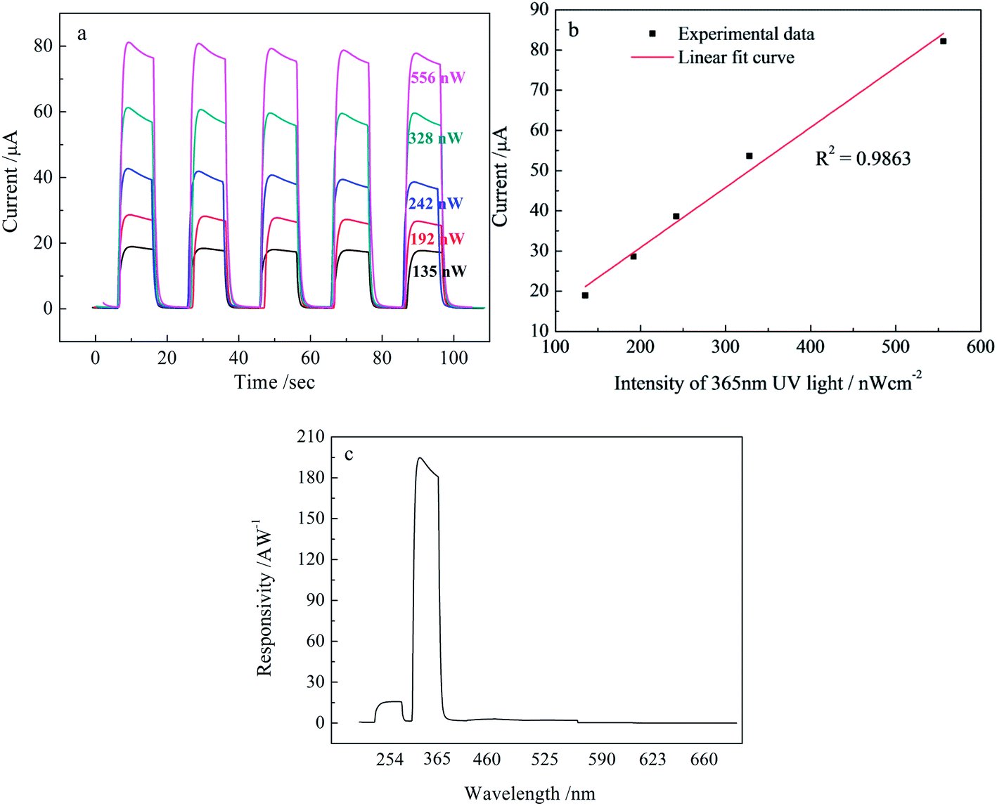
The dependence of the photocurrent on the incident light intensity shown in Fig. 7(a) gives another important characteristic of the TiO2-based UV PDs. The photocurrent increases with an increase in the UV light intensity from 135 to 556 nW cm−2. The linear fitting result shown in Fig. 7(b) shows a fabulous linear dependence of the photocurrent on the light intensity. It is worth noting that the TiO2 NR/NP-0.2 M-48 h-based UV PDs exhibit a photocurrent of ∼80 μA and a photosensitivity of ∼100 even at the ultralow light intensity of 135 nW cm−2, indicating an excellent UV response behavior under low light intensity. Fig. 7(c) and (d) shows the spectral response of TiO2 NR/NP-0.2 M-48 h at 1.0 V bias. From the figure, it is clearly seen that this UV PD has a peak response at 365 nm and a relatively low response at 254 nm, but almost no response at the visible light region from 460 to 660 nm, indicating an excellent UV light selectivity, which is in good agreement with the UV-Vis absorption of TiO2.
 | ||
| Fig. 7 Effect of UV light intensity and light wavelength on the photoresponse of TiO2 NR/NP-0.2 M-48 h sample at 1.0 V bias, (a and b) UV light intensity response curve, (c) spectral response curve. | ||
4 Conclusions
In summary, ordered TiO2 NR arrays on the FTO conductive glass have been synthesized by using a simple hydrothermal method. TiO2 NP-modified TiO2 NR hierarchical composites were obtained by the hydrolysis of TiCl4 at different concentrations and different reaction times. The TiO2 NPs not only deposited on the top surface of TiO2 NRs, but also filled the interface among the TiO2 NRs, due to the easy permeation of the TiCl4 solution. High TiCl4 concentration and long reaction time are favorable for the generation of more TiO2 NPs, which enhances the surface area of the composite. Compared with most other studies, the TiO2 NR/NP hierarchical composite-based UV PDs exhibit an extremely high responsivity and relatively fast response speed at the same time. Among the samples, TiO2 NR/NP-0.4 M-72 h based UV PD gives the highest responsivity of 1973 A W−1, the largest photosensitivity of 1158.9 and the fastest response speed (rise and decay times are 0.47 s and 1.02 s, respectively). The present high responsivity and relatively fast response speed are attributed to the large surface area generated by TiO2 NPs, the straight electron transport pathway offered from TiO2 NRs and the homojunction formed in the interface between TiO2 NRs and NPs. Furthermore, the excellent dependence of the photoresponse of the TiO2 composite on the light intensity and the fabulous UV light selectivity all make it a good candidate for UV light detection applications.Acknowledgements
The work was supported by the National Natural Science Fund for Distinguished Young Scholars of China (21125628) and the Fundamental Research Funds for the Central Universities (lzujbky-2013-61).Reference
- S. Kim, Y. T. Lim, E. G. Soltesz, A. M. DeGrand, J. Lee, A. Nakayama, J. A. Parker, T. Mihaljevic, R. G. Laurence, D. M. Dor, L. H. Cohn, M. G. Bawendi and J. V. Frangioni, Nat. Biotechnol., 2004, 22, 93 CrossRef CAS PubMed.
- M. Ettenberg, Adv. Imaging, 2005, 20, 29 Search PubMed.
- B. Tian, X. Zheng, T. J. Kempa, Y. Fang, N. Yu, G. Yu, J. Huang and C. M. Lieber, Nature, 2007, 449, 885 CrossRef CAS PubMed.
- Y. Bie, Z. Liao, H. Zhang, G. Li, Y. Ye, Y. Zhou, J. Xu, Z. Qin, L. Dai and D. Yu, Adv. Mater., 2011, 23, 649 CrossRef CAS PubMed.
- B. Tian and C. M. Lieber, Pure Appl. Chem., 2011, 83, 2153 CrossRef CAS PubMed.
- H. Xue, X. Kong, Z. Liu, C. Liu, J. Zhou and W. Chen, Appl. Phys. Lett., 2007, 90, 201118 CrossRef PubMed.
- X. Kong, C. Liu, W. Dong, X. Zhang, C. Tao, L. Shen, J. Zhou, Y. Fei and S. Ruan, Appl. Phys. Lett., 2009, 94, 123502 CrossRef PubMed.
- C. Lin, Y. Song, L. Cao and S. Chen, Nanoscale, 2013, 5, 4986 RSC.
- B. O'Regan and M. Gratzel, Nature, 1991, 353, 737 CrossRef CAS.
- P. Docampo, S. Guldin, M. Stefik, P. Tiwana, M. C. Orilall, S. HÜttner, H. Sai, U. Wiesner, U. Steiner and H. J. Snaith, Adv. Funct. Mater., 2010, 20, 1787 CrossRef CAS.
- Z. Lou, J. Deng, L. Wang, R. Wang, T. Fei and T. Zhang, RSC Adv., 2013, 3, 3131 RSC.
- J. Xing, H. Wei, E. Guo and F. Yang, J. Phys. D: Appl. Phys., 2011, 44, 375104 CrossRef.
- X. Li, C. Gao, H. Duan, B. Lu, Y. Wang, L. Chen, Z. Zhang, X. Pan and E. Xie, Small, 2013, 9, 2005 CrossRef CAS PubMed.
- M. Sun, X. Ma, X. Chen, Y. Sun, X. Cui and Y. Lin, RSC Adv., 2014, 4, 1120 RSC.
- X. He, C. Huz, B. Feng, B. Wan and Y. Tian, J. Electrochem. Soc., 2010, 157(11), J381 CrossRef CAS PubMed.
- T. Tsai, S. Chang, W. Weng, C. Hsu, S. Wang, C. Chiu, T. Hsueh and S. Chang, J. Electrochem. Soc., 2012, 159, J132 CrossRef CAS PubMed.
- J. Zou, Q. Zhang, K. Huang and N. Marzari, J. Phys. Chem. C, 2010, 114, 10725 CAS.
- B. Liu and E. S. Aydil, J. Am. Chem. Soc., 2009, 131, 3985 CrossRef CAS PubMed.
- S. Wang, W. Dong, R. Tao, Z. Deng, J. Shao, L. Hu, J. Zhu and X. Fang, J. Power Sources, 2013, 235, 193 CrossRef CAS PubMed.
- H. Peng, J. Li, S. Li and J. Xia, J. Phys. Chem. C, 2008, 112, 13964 CAS.
- E. Monroy, F. Omnes and F. Calle, Semicond. Sci. Technol., 2003, 18, R33 CrossRef CAS.
- K. Lv, M. Zhang, C. Liu, G. Liu, H. Li, S. Wen, Y. Chen and S. Ruan, J. Alloys Compd., 2013, 580, 614 CrossRef CAS PubMed.
- C. Soci, A. Zhang, X. Bao, H. Kim, Y. Lo and D. Wang, J. Nanosci. Nanotechnol., 2010, 10, 1 CrossRef PubMed.
- R. O'Hayre, M. Nanu, J. Schoonman and A. Goossens, J. Phys. Chem. C, 2007, 111, 4809 CAS.
- D. Cahen and G. Hodes, J. Phys. Chem. B, 2000, 104, 2053 CrossRef CAS.
- H. Yu, S. Zhang, H. Zhao and H. Zhang, Phys. Chem. Chem. Phys., 2010, 12, 6625 RSC.
- F. Guo and J. Huang, Proc. SPIE, 2012, 8373, 83732k1 CrossRef PubMed.
- H. Seong, J. Yun, J. Jun, K. Cho and S. Kim, Nanotechnology, 2009, 20, 245201 CrossRef PubMed.
| This journal is © The Royal Society of Chemistry 2014 |