
 Open Access Article
 This Open Access Article is licensed under a Creative Commons Attribution-Non Commercial 3.0 Unported Licence
Facile synthesis of BiSI and Bi13S18I2 as stable electrode materials for supercapacitor applications†
Huapeng
Sun
a,
Guiling
Yang
b,
Jie
Chen
a,
Caroline
Kirk
*a and
Neil
Robertson
 *a
*a
aSchool of Chemistry and EaStCHEM, University of Edinburgh, King's Buildings, David Brewster Road, Edinburgh, Scotland EH9 3FJ, UK. E-mail: Caroline.Kirk@ed.ac.uk; Neil.Robertson@ed.ac.uk
bHebei North university, Zhangjiakou 075000, Hebei, P. R. China
First published on 4th September 2020
Abstract
In this paper, we demonstrate a novel synthetic route of two bismuth chalcogenide materials 3-D hexagonal Bi13S18I2 and 3-D orthorhombic BiSI, and investigate their potential as the active electrode material for supercapacitors. Both pure BiSI and Bi13S18I2 powders were obtained for the first time at relatively low temperature (120 °C) in a solution system. We studied the effects of different reaction conditions on the surface morphology of the product and found that at a relatively low temperature of 120 °C under atmospheric pressure, the materials can yield smaller crystallite size and higher specific surface area, further increasing the capacitance compared to the synthesis under hydrothermal conditions. Cyclic voltammetry and galvanostatic charge–discharge measurements of the materials were studied using three-electrode and two-electrode configurations at a variety of currents. The galvanostatic charge–discharge measurement results show that the Bi13S18I2 electrode has a maximum areal capacitance of 247 mF cm−2 at the current density of 5 mA cm−2 and excellent capacitance retention of 98.4% after 5000 cycles at the current density of 50 mA cm−2 in 3.0 M KOH electrolyte as a two-electrode electrical double-layer capacitor system (EDLC). The BiSI and Bi13S18I2 powders have been characterized through PXRD, XPS, Raman spectroscopy, TGA–DSC, BET, SEM and TEM. This facile route to the synthesis of both Bi13S18I2 and BiSI with superior stability has promising potential for low-cost and effective electrochemical supercapacitor applications.
Introduction
In recent years, the demand for efficient, economical and environmentally-friendly energy storage systems for electronics, electric vehicles and smart sustainable energy grid applications has grown dramatically, and the design and development of sustainable energy storage devices has become an important research area.1–3 Supercapacitors and batteries are the most widely used in electronic devices and electric vehicles, in terms of the available different types of electrochemical energy storage devices. Traditionally, supercapacitors have been considered as power supplies with high power capability but low energy density when compared with batteries.4–6 Much effort has been put into improving the energy density of supercapacitors, in which asymmetric hybrid systems have been extensively studied by combining faradaic-type rechargeable battery electrodes with double-layer charge storage carbon electrodes.7–10 Bi-Based materials are considered as potential candidates for supercapacitors due to the low toxicity, high electrochemical stability, high redox reversibility and relatively high power. Specifically, Bi2O3 and Bi2S3 have been shown to have promise in supercapacitors and electrochemical devices.11–16 Bi2S3 is known to exhibit a very diverse range of crystal forms, including nanorods and nanoribbons that can be tuned to enhance the performance of the active electrode material in supercapacitors, generally in a pseudocapacitor mode.17–20 Among the common Bi-based chalcogenides, BiSI has been studied as a potential photovoltaic material due to its n-type semiconductor properties and high absorption coefficient. However, the possibility of BiSI in capacitor applications has not been studied. In addition, the manufacture of bismuth chalcogenides typically requires high annealing temperatures and a multi-step procedure, which makes economic feasibility very low. For example, synthesis of BiSI required a Pyrex tube which was flame-sealed under vacuum while in an ice bath to prevent loss of I2 vapor or to be heated to 900 K.21–26 Recently, a solvothermal synthesis route was reported, however this still requires sealed and pressure conditions.27To the best of our knowledge, a simple one-step, moderate-temperature solution synthesis route has not been reported.
In this paper, we report the controlled synthesis of two different bismuth chalcogenide materials, BiSI and Bi13S18I2, from solution in a single and facile step. Their electrochemical performance as electrode materials for supercapacitors was tested in 3.0 M KOH electrolyte, using both a three-electrode system and a two-electrode electrical double-layer capacitor (EDLC) system. Improved supercapacitor performances were shown by the materials prepared in an open beaker under mild conditions (BiSI-b, Bi13S18I2-b) compared with control samples prepared in an autoclave (BiSI-a, Bi13S18I2-a). Operating as a pseudocapacitor, the BiSI-b electrode shows the highest specific capacitance of 128 F g−1 among four prepared electrodes at a current density of 2.0 A g−1 and excellent capacitance retention of 78.5% over 2000 cycles at a current density of 10.0 A g−1 in a three-electrode system. The Bi13S18I2-b electrode as the active material in EDLC-type supercapacitors achieved a superior cycle stability with 98.4% capacitance retention after 5000 cycles at a current density of 50 mA cm−2 and a highest areal capacitance of 247 mF cm−2 at a current density of 5 mA cm−2. This is more than 4 times higher compared with our previously reported thin-film Bi13S18I2 electrode28 (53.65 mF cm−2 at 2 mA cm−2).
Results and discussion
The two bismuth chalcogenide iodide materials, labelled BiSI-b and Bi13S18I2-b, were prepared by a novel one step synthesis route at relatively low temperatures in an open beaker, as described in the Experimental section. For comparison we will also present results from the same materials synthesized using an autoclave at 160 °C, and labelled BiSI-a and Bi13S18I2-a. Fig. 1A shows PXRD patterns of the as-prepared materials BiSI-a and BiSI-b and confirms both samples contain BiSI. Refinement of the PXRD data using a least squares refinement procedure was carried out in space group Pnam. The refined unit cell parameters for BiSI-a are a = 8.501(3) Å, b = 10.244(4) Å and c = 4.172(2) Å and for BiSi-b, a = 8.497(2) Å, b = 10.243(3) Å and c = 4.171(2) Å. These are in in good agreement with standard literature values (a = 8.5138 Å, b = 10.2639 Å and c = 4.1742 Å), (ICDD PDF card no. 43-652).29 The samples generally showed very good phase purity, although for the BiSI-a sample, weak diffraction peaks at 15.7°, 23.7°, 24.9° and 28.6° were also observed, which can be matched to the presence of Bi2S3 as a minor impurity phase. | ||
| Fig. 1 PXRD patterns of the as-prepared BiSI powder (A) and Bi13S18I2 powder (B). | ||
Comparison of the PXRD patterns of the Bi13S18I2-a and Bi13S18I2-b to a standard pattern are shown in Fig. 1B. Both datasets were refined using a least squares refinement procedure in the primitive trigonal space group P3, with the refined unit cell parameters for Bi13S18I2-a: a = 15.634(6) Å, and c = 4.014(2) Å, and for Bi13S18I2-b: a = 15.63(2) Å, and c = 4.011(3) Å. The refined values are in good agreement with values published by Groom et al. (a = 15.612 Å, and c = 4.0168 Å, ICSD collection number 243730).21 The PXRD pattern collected on Bi13S18I2-a had the presence of weak impurity peaks at 15.7°, 22.4° and 25.2° 2θ, which could be attributed to the presence of Bi2S3. Bi13S18I2 has been previously reported as having the formula [Bi(Bi2S3)9I3]2/3,30 Bi19S27I326 and Bi13S18I225 we adopted the formula Bi13S18I221 which contains [Bi2]4+ dimers and its unit cell is shown in Fig. S1 (ESI†).
We also analyzed the products from syntheses of the BiSI material carried out at different temperatures, 60 °C, 90 °C, 120 °C and 150 °C, using PXRD and the data are presented in Fig. S1 (ESI†). This shows that at a lower synthesis temperature of 60 °C, Bi3+ ions react directly with I− and oxygen in the air, forming BiOI rather than BiSI. As the temperature rises, Bi3+ starts to react with thioacetamide to form BiSI; at 90 °C the product is a mixture of BiOI and BiSI. When the reaction temperature is too high, reaching 150 °C, the decomposition of thioacetamide is too fast, and only Bi2S3 is formed. Only controlling the temperature at 120 °C for 1 hour was found to form pure BiSI without the presence of BiOI or Bi2S3. The suggested synthesis route is:
| Bi3+ + CH3C(S)NH2 + H2O + I− → BiSI + CH3C(O)NH2 + 2H+ |
Fig. 2 shows SEM images of BiSI and Bi13S18I2 samples, with both having needle-like morphologies. BiSI-a presents as bundles of needles, with each needle having a length of 10 to 30 μm, whereas for BiSI-b, the needles are dispersed, and each needle has a length of about 1 to 2 μm, much smaller than the length of the BiSI-a needles. As shown in Fig. 2A, the morphology of Bi13S18I2-a can be described as flower-like, formed by needle-like branches, each of which has a length of about 1 to 2 μm. This significantly increases the specific surface area when compared to the BiSI samples. A flower-like microstructure is reported to allow the construction of high performance electrodes because of the significant connection between the crystallites, which will facilitate the conduction of charge in the active material layer.31 Bi13S18I2-b also shows a flower-like morphology similar to Bi13S18I2-a, not formed by needles, but instead through interconnection of sheet-like nanoparticles of around 60 nm length. This special three-dimensional flower shape not only increases the specific surface area, but also improves the performance as supercapacitor (vide infra); the interstitial spaces between the nanoparticles in the structure can provide more channels for electrolyte ions to access and more electroactive sites, while the sheet structure formed by the nanorods can reduce the internal resistance.32
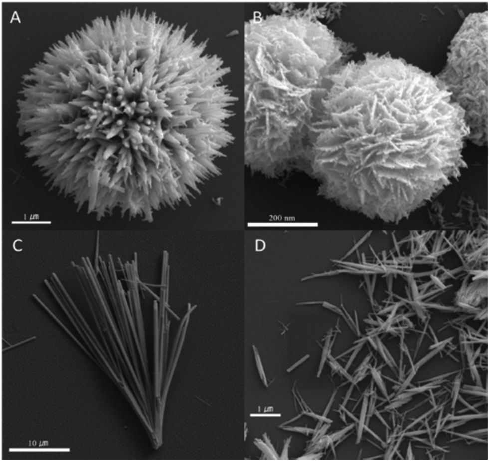 | ||
| Fig. 2 SEM micrographs of, Bi13S18I2-a (A) and Bi13S18I2-b (B) BiSI-a (C), BiSI-b (D). | ||
TEM was used to study the morphology of BiSI-b and Bi13S18I2-b in more detail, (Fig. 3). It can be clearly seen that BiSI-b has a single needle like morphology with a length of around 550 nm. The high resolution TEM image presented in Fig. 3B of BiSI-b clearly shows two different sets of lattice fringes, with measured interplanar spacings of 0.30 nm, corresponding to the (121) crystallographic plane of BiSI, and 0.44 nm, corresponding to the (120) crystallographic plane. These are two of the most intense reflections observed by PXRD (Fig. 1). The corresponding selected-area electron diffraction (SAED) patterns of BiSI-b (inset in Fig. 3B) shows that the BiSI-b sample has a 3-D orthorhombic structure. It can be seen from Fig. 3D that the sheet-like structure of Bi13S18I2-b is formed by nanorod with a length from 50 nm to 120 nm. The high resolution TEM image of Bi13S18I2-b, presented in Fig. 3F, shows a single crystallographic plane (130) with a measured interplanar spacing of 0.375 nm, consistent with the most intense reflection observed by PXRD (Fig. 1). The corresponding SAED pattern (inset in Fig. 3E) shows a 3-D hexagonal structure indicated good crystallinity. The corresponding Bi, S and I elemental maps in Fig. 3G and H, show the three elements are very uniform, further demonstrating the homogeneous growth of pure BiSI and Bi13S18I2 crystals during synthesis instead of a mixture of different materials containing these elements in different proportions.
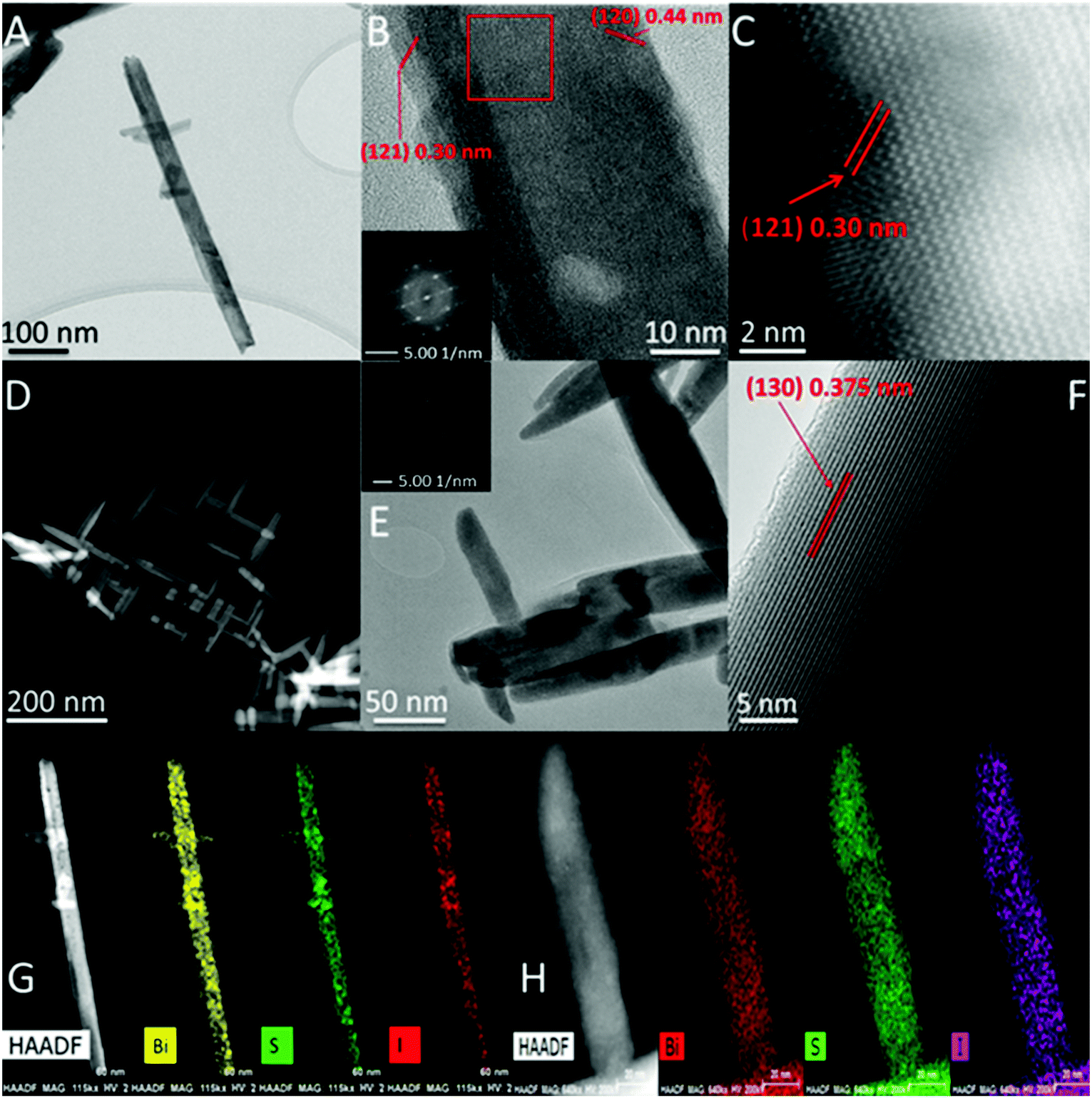 | ||
| Fig. 3 TEM images of BiSI-b (A and B) and Bi13S18I2-b (D and E) and HRTEM images of BiSI-b and Bi13S18I2-b (C from the red square of image B and F from the red square of image E), with their corresponding elemental maps BiSI-b (G) and Bi13S18I2-b (H) respectively. | ||
Raman spectra were collected on several samples of BiSI-b and Bi13S18I2-b over the wavenumber range 60–500 cm−1 and sample datasets are shown in Fig. 4. Both BiSI-b and Bi13S18I2-b show low energy Bi–S vibrational modes at 220 cm−1 and 280 cm−1, which are similar to Bi2S3.33 Kalpen et al. reported that a Bi−Bi stretching mode can be observed between 102 and 108 cm−1 due to the presence of Bi24+ dimers.33 A strong peak is observed at 106 cm−1 in the spectrum of Bi13S18I2-b, confirming the presence of Bi24+ dimers in this structure. The comparison of BiSI-a, BiSI-b, Bi13S18I2-a and Bi13S18I2-b (Fig. S2, ESI†) shows that both synthetic routes give similar spectra, and the bands observed fit with those for Bi–S and Bi–Bi for the BiSI and Bi13S18I2 phases.
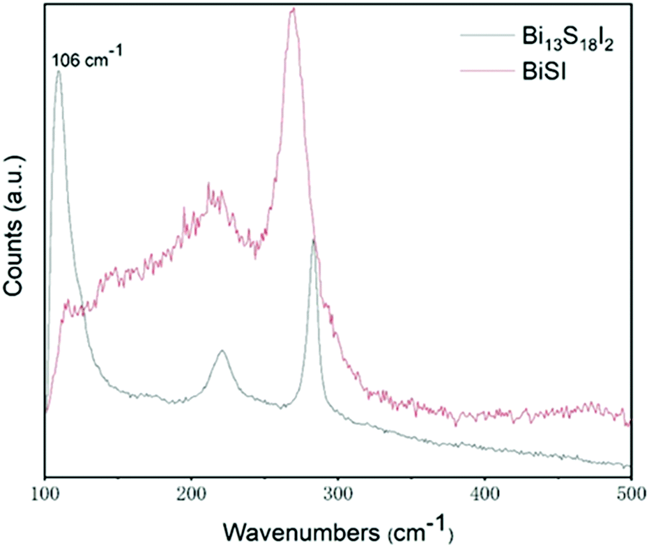 | ||
| Fig. 4 Raman spectra of BiSI-b and Bi13S18I2-b. | ||
Thermogravimetric analysis (TGA) was carried out to confirm the purity of prepared BiSI and Bi13S18I2 samples. The TGA data collected on heating BiSI-b and Bi13S18I2-b samples to 800 °C under a nitrogen gas flow, are presented in Fig. 5 and their DSC–TGA data are shown in Fig. S3 (ESI†). The TGA data collected on BiSI show that the decomposition has three distinct stages; the first stage is between 370 °C and 440 °C, the second stage is between 440 °C and 595 °C and the third stage occurs above 595 °C. The decomposition of Bi13S18I2 has two stages which are consistent with the second and third decomposition stages of BiSI. To monitor the decomposition processes and determine the phases that form on heating both of these materials, PXRD data were collected on separate samples that were heated to 440 °C and 600 °C, which were found to be temperatures where weight loss events occurred during the TGA experiments. The results from analysis of the PXRD data collected on samples from the ex situ heating experiments show that at 440 °C, BiSI has transformed to Bi13S18I2 and its PXRD pattern is shown in Fig. S4 (ESI†). When Bi13S18I2 was heated to 600 °C, it decomposes to Bi2S3, which also requires a redox reaction to convert Bi2+ to Bi3+. This disproportionation reaction produced Bi and Bi2S3 and BiI3. PXRD data which were collected at 600 °C are shown in Fig. S4 (ESI†), indicating that Bi2S3 and Bi were formed. After heating to 800 °C and cooling to room temperature, only small white metallic balls remained. The decomposition reactions of the three stages are:
| 36BiSI(s) → 2Bi13S18I2(s) + 10BiI3(g) + I2(g) | (1) |
| 3Bi13S18I2(s) → 18Bi2S3(s) + 2BiI3(g) + Bi(l) | (2) |
| Bi2S3(s) → 2Bi(l) + 3S(g) | (3) |
 | ||
| Fig. 5 TGA data collected on BiSI-b and Bi13S18I2-b under a Nitrogen gas flow. | ||
The experimental weight loss values and the theoretical weight loss values, calculated from the above three equations, are shown in Table S1 (ESI†). It can be seen that the experimental weight loss values are consistent with the theoretical calculated values, which confirms the decomposition steps outlined above.
Fig. 6 presents the X-ray photoelectron spectra (XPS) of BiSI and Bi13S18I2 powders. Comparing the Bi 4f orbital bonding energy of Bi13S18I2 with BiSI, the values are shifted to lower energy, whereas the bonding energy of S 2s is shifted to higher energy from 225.83 eV to 227.31 eV. Table S2 (ESI†) tabulates the observed experimental atomic percentages of specific bismuth, iodine, and sulfur in the powder and the values agree closely with the theoretical atomic composition of BiSI and Bi13S18I2. This indicates high purity BiSI and Bi13S18I2 materials have been synthesized.
 | ||
| Fig. 6 High resolution X-ray photoelectron spectrum of Bi 4f (A), S 2p (B) and I 3d (C) for BiSI-b and Bi13S18I2-b powder; specific peaks are labelled. | ||
Typical nitrogen adsorption–desorption isotherms for BiSI and Bi13S18I2 powder are shown in Fig. 7. After analysis based on the Brunauer–Emmett–Teller (BET) equation:34

 | ||
| Fig. 7 Nitrogen adsorption–desorption isotherms (A) and pore size distribution (B) for BiSI and Bi13S18I2 powder. | ||
The BiSI and Bi13S18I2 samples were first tested as electrode materials for supercapacitors using a three-electrode system at room temperature, which is appropriate to give an overview of processes at different potentials. Fig. 8A and C show a series of CV profiles measuring the BiSI-b sample over a potential window of −1.0 to 0 V vs. Ag/AgCl with scan rates from 10 to 100 mV s−1. At more negative potentials, the CV profiles are different to the conventional rectangles for EDLC, suggesting pseudo-capacitive features. CV profiles consist of one reduction peak and two oxidation zones. In detail, for the case of low scan rate of 10 mV s−1, the reduction peak (R1) is located at −1 V, which is caused by the reduction of Bi3+ to Bi; furthermore, there are two oxidation peaks; O1 at −0.62 V and O2 at −0.42 V. These can be assigned to the oxidation process of Bi° → Bi+ and Bi+ → Bi3+, respectively.36,37 With increasing scan rate, the CV curve of sample BiSI-b shows oxidation peaks shifting to a more positive potential while reduction peaks shift to a more negative potential, as shown in Fig. 8A. This phenomenon is very common for CV curves, mainly derived from their iR drops or ion diffusion.38
 | ||
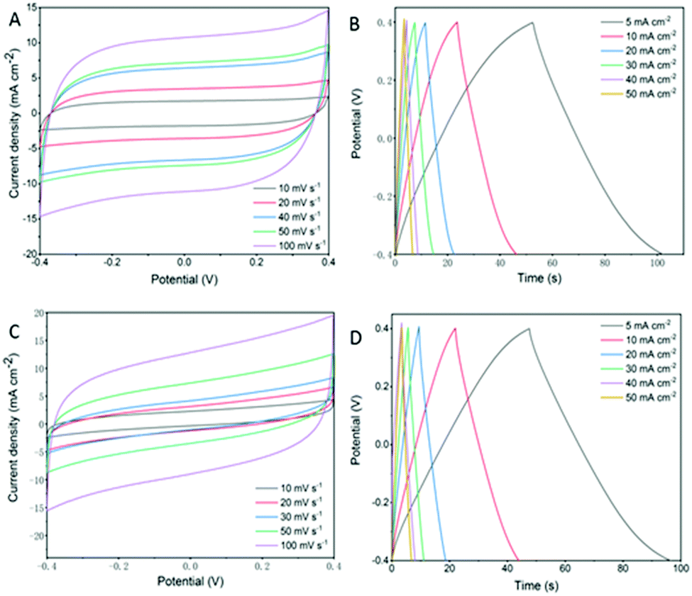
| Fig. 8 Cyclic voltammograms collected at different scan rates for BiSI-b and Bi13S18I2-b electrode (A and C) and their charge–discharge curves at various current densities (B and D). | ||
Fig. 8B displays overall galvanostatic charge–discharge (GCD) profiles of the BiSI-b sample at various current densities, between 2 and ∼10 A g−1, while designating a potential window of −1.0 to ∼0 V. GCD profiles present unique charging–discharging features, with asymmetric curves differing from typical triangular outlines, which indicate pseudo-capacitive characteristics. For the dis-charging stage, there are two quite distinct processes including a steep voltage drop and gradual voltage drop. The former steep voltage drop is very different to the triangular outline, probably due to the internal resistance, while the latter originated from the involvement of a quasi-faradaic process in the sample. Other kinds of bismuth-based compounds, such as Bi2O314 and SWCNT/BiVO439 composites, are also reported to exhibit approximate pseudo-capacitive GCD behaviour. The specific capacitances were also calculated from the slope of the discharge curves according to:40
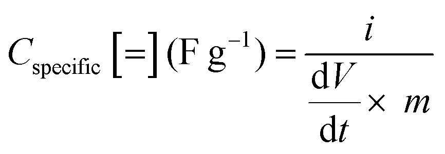
where i is the constant current (A), dV/dt is the slope of the discharge curve taken in the voltage range 0–1 V for consistency, area is the average geometric area of the two electrodes (cm2) and m is combined mass of the active material on the working electrode (g). The specific capacitances of the BiSI-b electrode were 128 F g−1, 121 F g−1, 106 F g−1, 100 F g−1 and 90 F g−1 with increasing current densities from 2 A g−1 to 10 A g−1, which suggests that the specific capacitance of the electrode decreases with increase in current density. The specific capacitances of the Bi13S18I2-b electrode were 86 F g−1, 78 F g−1, 76 F g−1, 72 F g−1 and 59 F g−1 with increasing current densities from 2 A g−1 to 10 A g−1.

To further investigate the electrochemical performance, the prepared BiSI and Bi13S18I2 samples were tested under a two-electrode system at room temperature, which is the configuration of an actual supercapacitor device. As shown in Fig. 9, the CV and GCD curves measured in the two-electrode system showed significant changes in shape compared with those achieved in the three-electrode system (Fig. 8), and the CV showed significant rectangular features. This is due to the controlled voltage range such that we are no longer scanning into the range where faradaic processes occur. GCD shows a distinct triangle, which is a feature of EDLC, free of faradaic processes that generally lead to poor stability. The area and specific capacitance of the device were calculated. When the scan rate was increased from 0.01 V s−1 to 0.1 V s−1, the capacitance of the electrode was reduced. The reduction in capacitance is a common feature of EDLC, which is caused by different time states of charge transport and ion diffusion at different scan rates. At lower scan rates, the electrolytic ions have enough time to diffuse into the pores in the active material layer, increasing charge build up and increasing capacitance. At higher scan rates, charge accumulation is limited to the electrode surface, reducing the capacitance of the electrode.
 | ||
| Fig. 9 Cyclic voltammograms collected at different scan rates for BiSI-b and Bi13S18I2-b electrode as EDLC (A and C) and their charge–discharge curves at various current densities (B and D). | ||
The galvanostatic charge–discharge measurements were carried out over a −0.4 to 0.4 V window, with current densities varying from 5 mA cm−2 to 50 mA cm−2 (Fig. 9B and D). The charge–discharge curves of Bi13S18I2-b and BiSI-b electrodes are largely symmetric and the discharge curve displays remarkable linearity following an initial iR drop even at the lowest current densities, corroborating the non-faradaic EDLC behaviour. The areal capacitances of the BiSI-b device were from 168 mF cm−2 to 99 mF cm−2, and the specific capacitances of the Bi13S18I2-b device were 247 mF cm−2 to 202 mF cm−2 with increasing current densities from 5 mA cm−2 to 50 mA cm−2. The energy density and power density calculated from galvanostatic charge and discharge measurements are summarized in Table S3 (ESI†), which shows that the BiSI-b electrode has a calculated energy density of 22.2 W h kg−1 with a high power density of 3.15 kW kg−1 as a pseudo-capacitor, and the Bi13S18I2-b electrode shows a calculated energy density of 2.7 W h kg−1 with a high power density of 3.98 kW kg−1 as EDLC.
The comparison of specific capacitance of four BiSI and Bi13S18I2 electrodes in pseudo-capacitor system is shown in Fig. 10A and areal capacitance in EDLC system is shown in Fig. 10B at different discharge current density. Fig. 10B shows that compared with BiSI electrodes, both samples of Bi13S18I2 prepared as electrodes have much larger areal capacitance and better capacitance retention with increased discharge current density, especially so for sample Bi13S18I2-b. Electrochemical performance is affected by the electrode morphology and the size of the active material. Nanoparticles of about 20 nm can increase the capacitance of EDLC.41 From the SEM image, we have shown that Bi13S18I2-b particles have the smallest size of around 40 nm, which can effectively shorten the nanoscale electron diffusion length during the charge and discharge process. This will improve the electrochemical utilization rate, the interface contact and reduce the internal resistance. At the same time, the large surface area is beneficial to increase the capacitance of the EDLC. Bi13S18I2-b has the largest surface area of the four electrodes tested here, which may be another important factor to improve its capacitance. Comparing the two synthetic routes, the capacitance of the two samples (BiSI-a and Bi13S18I2-a) synthesized by a hydrothermal method at 160 °C is smaller than the same component yielded by our facile solution reaction route at 120 °C.
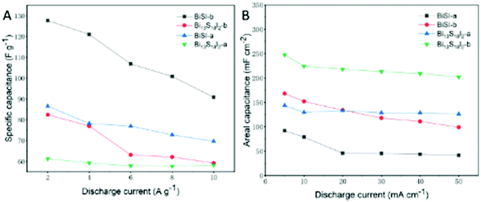 | ||
| Fig. 10 Variation of specific capacitance of BiSI-a, BiSI-b, Bi13S18I2-a and Bi13S18I2-b electrodes at different discharge current density in pseudo-capacitor system (A) and EDLC system (B). | ||
The long term cyclic stability of a series of BiSI and Bi13S18I2 EDLC electrodes was measured by the galvanostatic charge/discharge technique at a constant current density of 10 A g−1 over 5000 cycles, and the data are shown in Fig. S6 (ESI†). The specific capacitance of four electrodes all remained over 98% of the initial capacitance after 5000 cycles, which indicated they have remarkable cycle stability at high current conditions over long charge/discharge processes, especially for the Bi13S18I2-a sample, which retained 99.2% of its initial capacitance. The PXRD patterns of the BiSI-b and Bi13S18I2-b electrodes before and after 5000 charge/discharge cycles as EDLC using two electrodes (2E) and pseudo-capacitor using three electrodes (3E) are compared in Fig. 11, and other electrodes are shown in Fig. S6 (ESI†). It can be clearly seen that the PXRD patterns of both BiSI and Bi13S18I2 electrode as EDLC (2E) have not significantly changed after 5000 cycles, indicating much of the starting bismuth sulfide iodide materials remain, especially for the Bi13S18I2-b sample. However, the PXRD patterns of the electrodes, when operated as a pseudo-capacitor (3E) by using a larger voltage range, shows that most of the BiSI and Bi13S18I2 peaks have disappeared and new peaks are observed due to the formation of Bi during a faradaic reaction. SEM images of Bi13S18I2-b electrode after undergoing the 5000 cycles as EDLC indicate that the surface coverage of the carbon paper with the activated Bi13S18I2 remained largely the same after cycling (Fig. S7, ESI†). Moreover, the EDS results in Fig. S7 (ESI†) of three points on the electrode after 5000 EDLC cycles, show that the elemental composition of the active material on the electrode surface is basically the same as before the cycling. This proves that there is no chemical reaction process during the charge/discharge cycle, resulting in its excellent capacitance retention. This is consistent with the results from analysis of PXRD data and SEM images on the Bi13S18I2 material after 5000 cycles. Conversely, the SEM image of electrodes after 2000 pseudo-capacitor cycles (Fig. S7, ESI†) shows that the ∼1 μm length needle-like Bi13S18I2 structure has disappeared and has been replaced by nanoparticles of around 300 nm. Further EDS results (Fig. S7, ESI†) shows that the peaks relating to the presence of S and I disappear, with only the peaks relating to the presence of Bi remaining. This is consistent with the results from analysis of PXRD data and SEM images and is explained by the significant decrease of stability caused by the irreversible faradaic reaction in the pseudo-capacitor system.
 | ||
| Fig. 11 PXRD patterns of (blue) as-prepared BiSI-b and Bi13S18I2-b electrode on carbon paper and the electrodes after 2000 cycles (in three electrodes) and 5000 cycles (in two electrodes) stability test. Standard BiSI: ICDD PDF card no. 45-652 and Bi13S18I2: ICDD PDF card no. 73-1157. | ||
Electrochemical impedance spectroscopy (EIS) was carried out in the three-electrode test system to characterize the physical and electrochemical processes of the BiSI and Bi13S18I2 electrodes as supercapacitors in response to AC currents at different frequencies. All EIS measurements were conducted at their open circuit potential with an AC amplitude of 10 mV at a frequency of 150 kHz to 0.1 Hz. The Nyquist plot of the BiSI and Bi13S18I2 electrodes both show a typical faradaic pseudocapacitance behavior with a semicircle in the high frequency region, and a line towards vertical in the low frequency region in Fig. 12A, which is close to a mixture of typical battery characteristic and capacitor behaviour.42 The intercept of the semicircle at the high frequency end of the real axis (Z′) gives the value of Rs in the equivalent circuit, indicating the combined resistance due to the resistance in the KOH electrolyte and the current collector. This is usually referred to as the equivalent series resistance (ESR). Since all charge transfer during charge–discharge occurs through the electrolyte, Rs is connected in series with other circuit components and found to be approximately 1.24 Ω to 1.52 Ω. The diameter of the semicircle and curvature are simulated with resistor Rct in parallel with a constant phase element Cdl to indicate two possible behaviors of the electrolyte during charging and discharging. At moderate frequencies, the ions penetrate the active layer of the electrodes, introducing Rct with a calculated value of 3.01 Ω (Bi13S18I2-b), 3.22 Ω (BiSI-b), 3.52 Ω (Bi13S18I2-b after 2000 cycles) and 3.94 Ω (BiSI-b after 2000 cycles), which was analysed based on the diameter of semicircle, representing the charge transfer resistance and the bulk resistance of the active material and electrode pores. The Rct of Bi13S18I2 electrode is smaller than the BiSI electrode, which may be due to the smaller particle size of Bi13S18I2 leading to smaller bulk resistance. At lower frequencies, the ions can diffuse into the narrow pores of the porous electrode and the slope of the line represents diffuse layer resistance including double layer formation and ion diffusion process. Nyquist plots of the BiSI and Bi13S18I2 electrodes both show typical EDLC behaviour in EDLC test system with quasi-vertical line in Fig. 12B.43–45 It can be seen from the enlarged image of high frequency area in Fig. 12B that both BiSI-b and Bi13S18I2-b have a very small semicircle and its diameter is assigned to the electrolyte resistance in the pores of the electrodes.46 After 5000 cycles, the Nyquist plot of both BiSI-b and Bi13S18I2-b are basically the same as before the cycles, indicating good cycle stability. The electrolyte resistance in the pores of the electrodes slightly increased after cycles. This may be because the electrolyte enters the lattice of the electrode material during the cycling process, which reduces the conductivity of the electrode material in the pore of the electrodes.
 | ||
| Fig. 12 Experimental Nyquist plots of BiSI-b and Bi13S18I2-b electrodes before and after 2000 cycles in tree electrodes system (A) and after 5000 cycles in EDLC system (B), with equivalent circuit inserted. | ||
Conclusions
We have demonstrated the first low-temperature, and solution-based synthesis of the bismuth chalcogenide materials, BiSI and Bi13S18I2. We systematically studied the effect of reaction temperature and time on the reaction product and found the optimum reaction conditions for the synthesis of pure BiSI and Bi13S18I2 powders is at 120 °C for one hour. We have characterized the electrodes to show the potential range of both faradaic pseudo-capacitances and non-faradaic EDLC behaviour using a mass load (4–5 mg cm−2) of BiSI and Bi13S18I2 active materials and 3 M KOH as the electrolyte. In two-electrode devices, all BiSI and Bi13B18I2 EDLCs have excellent capacitance retention, especially the Bi13B18I2 capacitor, which has a capacitance of 247 mF cm−2 at the current density of 5 mA cm−2 and an excellent capacitance retention of 98.4% after 5000 cycles. Furthermore, all samples formed using our straightforward, ambient-pressure synthetic route have higher specific surface area and higher specific capacitance than the samples using a hydrothermal route at high pressure. For the first time, we have shown that BiSI and Bi13S18I2 materials can be integrated into low-cost promising energy storage devices with excellent long-term cycle stability and we have removed the need for high pressure and high temperature to synthesise BiSI and Bi13S18I2, making large-scale industrial production possible. In addition, this new synthesis route allows much further optimization to be carried out through blending these bismuth chalcogenide materials with other materials, optimizing the electrolyte and making asymmetric supercapacitors to further enhance the performance.Experimental
Synthesis and characterization
All reagents were obtained from commercial suppliers (Acros Organics, Sigma Aldrich, Fluka) and used as received unless otherwise stated. Solvents used were of analytical grade (Sigma Aldrich, Fisher Scientific, VWR Chemicals, and Cambridge Isotope Laboratories).Two different routes were used to synthesize BiSI. First, 4.4 g (58 mmol) thiourea and 5.1 g (20 mmol) I2 were mixed and ground in a mortar and pestle for 20 minutes. This powder mixture and 9.7 g (20 mmol) Bi(NO3)3·5H2O were transferred to a 100 mL Teflon-lined autoclave with 60 mL deionized water. The autoclave was heated to 160 °C for 15 hours and was then cooled to room temperature. The final product was washed and centrifuged several times with ethanol and deionized water until the liquid became clear. The precipitate was dried in an oven at 70 °C for 8 hours. The product of this route will be known as BiSI-a with a yield of 71%. The second route is to dissolve 0.485 g (1.0 mmol) Bi(NO3)3·5H2O in 20 mL deionized water and heat to 120 °C. This solution was slowly added to a mixture of 0.17 g (1.0 mmol) KI and 0.2 g (2.7 mmol) thioacetamide (TAA) in 20 mL deionized water which was already heated to 120 °C. The pH value of the solution was adjusted to 1 by acetic acid. After heating for 1 hour at 120 °C, the precipitate was washed and dried using the same process as the first route and the final product will be known as BiSI-b with a yield of 82%.
Two different synthetic routes were also employed to synthesize Bi13S18I2. First, 1.27 g (0.5 mmol) I2 were ground for 5 minutes. This I2 powder, 4.56 g (0.06 mmol) thiourea and 9.7 g (2.0 mmol) Bi(NO3)3·5H2O were transferred to a 100 mL Teflon-lined autoclave with 40 mL deionized water. The autoclave was heated to 160 °C for 15 hours and then cooled to room temperature. The final product was washed and centrifuged several times with ethanol and DI water until the liquid became clear. The precipitate was dried in an oven at 70 °C for 8 hours and will be known as Bi13S18I2-a with a yield of 68%. The second route for synthesis of Bi13S18I2 was to dissolve 0.485 g (1.0 mmol) Bi(NO3)3·5H2O in 20 mL DI water to form a suspension and heated to 120 °C. The suspension was slowly added to a mixture of 0.03 g (0.18 mmol) KI and 0.2 g (2.7 mmol) thioacetamide (TAA) in 20 mL deionized water in a 100 mL beaker which was already heated to 120 °C. The pH of the solution was adjusted to 1 by acetic acid. After heating the solution for 1 hour at 120 °C, the precipitate formed was washed and dried using the same process as the first route and the final product was marked as Bi13S18I2-b with a yield of 77%.
Powder X-ray diffraction (PXRD) data were collected using a Bruker (D2 Advance) diffractometer with Cu-Kα radiation (λ = 1.5418 Å), at room temperature over a 2-theta range of 5° to 60°, with a stepsize of 0.1° and a count time of 0.45 s per step. X-ray photoelectron spectra were acquired using a Thermo Scientific (VG Sigma Probe) XPS spectrometer with monochromatic Al-Kα as the source of X-rays. Scanning electron microscopy was carried out using a Zeiss (SIGMA HD VP) Field Emission-Scanning Electron Microscope (SEM) operating with an accelerating voltage of 10 kV. Transmission Electron Microscopy (TEM) and Electron Dispersive Spectroscopy (EDS) were carried using a FEI Titan Themis microscope operating with an accelerating voltage of 200 kV. Nitrogen adsorption experiments were carried out to determine specific surface areas of the samples using a JWGB SCI. & TECH BK132F automatic adsorption instrument. Raman spectra were acquired using a Renishaw in Via Raman Microscope with an excitation laser wavelength of 785 nm and a spectral resolution of approximately 1 cm−1. The TGA–DSC experiments were carried out using a TA Instruments SDT Q600, samples were heated from room temperature to 800 °C under flowing Nitrogen with a ramp rate of 10 degree per minute.
Measurement of electrochemical properties
The working electrodes for both the three electrodes system and two-electrode EDLC system were prepared by mixing BiSI and Bi13S18I2 powder with activated charcoal powder and PTFE powder in 1 mL ethanol as the solvent to make a final Bi13S18I2![[thin space (1/6-em)]](https://www.rsc.org/images/entities/char_2009.gif) :charcoal:PTFE mixture with a weight ratio of 85:10:5. The resulting suspended solution was sonicated until homogenized, and around 200 μL was drop-coated onto 1 cm2 conductive carbon paper (ELAT, NuVant Systems Inc.) substrate and dried at 90 °C for 6 hours. The active mass of deposited BiSI-a, BiSI-b, Bi13S18I2-a and Bi13S18I2-b electrodes were 4.4 mg, 4.0 mg, 4.5 mg and 4.4 mg, respectively, used for all subsequent calculations. When assembling the EDLC, two coated electrodes were separated by a thin polymer separator (Celgard 3501) pre-soaked in a 3.0 M KOH aqueous electrolyte solution and then sandwiched in a symmetrically-assembled capacitor test cell (ECC-std, EL-CELL GmbH). In the three-electrode system, Ag/AgCl (3.0 M KCl) and a Pt wire were used as the reference and counter electrode, respectively with 3.0 M KOH aqueous electrolyte. Cyclic voltammetry (CV), galvanostatic charge/discharge measurements and electrochemical impedance spectroscopy (EIS) were carried out using an Autolab electrochemical work station with FRA2 module using General Purpose Electrochemical System (GPES) and Frequency Response Analyser (FRA) software.
:charcoal:PTFE mixture with a weight ratio of 85:10:5. The resulting suspended solution was sonicated until homogenized, and around 200 μL was drop-coated onto 1 cm2 conductive carbon paper (ELAT, NuVant Systems Inc.) substrate and dried at 90 °C for 6 hours. The active mass of deposited BiSI-a, BiSI-b, Bi13S18I2-a and Bi13S18I2-b electrodes were 4.4 mg, 4.0 mg, 4.5 mg and 4.4 mg, respectively, used for all subsequent calculations. When assembling the EDLC, two coated electrodes were separated by a thin polymer separator (Celgard 3501) pre-soaked in a 3.0 M KOH aqueous electrolyte solution and then sandwiched in a symmetrically-assembled capacitor test cell (ECC-std, EL-CELL GmbH). In the three-electrode system, Ag/AgCl (3.0 M KCl) and a Pt wire were used as the reference and counter electrode, respectively with 3.0 M KOH aqueous electrolyte. Cyclic voltammetry (CV), galvanostatic charge/discharge measurements and electrochemical impedance spectroscopy (EIS) were carried out using an Autolab electrochemical work station with FRA2 module using General Purpose Electrochemical System (GPES) and Frequency Response Analyser (FRA) software.
Conflicts of interest
The authors state there are no conflicts to declare.Acknowledgements
We thank Dr Aaron Naden for performing the SEM and TEM measurements in the University of St. Andrews. We thank Dr Stephen Francis for help in performing XPS measurements. We thank Dr Andrey Gromov for the help of performing Raman measurements. We thank Dr Dimitrios Kampouris for the fruitful discussion.Notes and references
- C. Guan, X. Liu, W. Ren, X. Li, C. Cheng and J. Wang, Adv. Energy Mater., 2017, 7, 1602391 CrossRef.
- M. Hannan, M. Hoque, A. Mohamed and A. Ayob, Renewable Sustainable Energy Rev., 2017, 69, 771–789 CrossRef.
- M. B. Tayel, M. M. Soliman, S. Ebrahim and M. E. Harb, J. Electron. Mater., 2016, 45, 820–828 CrossRef CAS.
- J. Zhou, H. Zhao, X. Mu, J. Chen, P. Zhang, Y. Wang, Y. He, Z. Zhang, X. Pan and E. Xie, Nanoscale, 2015, 7, 14697–14706 RSC.
- L. Feng, Y. Zhu, H. Ding and C. Ni, J. Power Sources, 2014, 267, 430–444 CrossRef CAS.
- M. M. Sk, C. Y. Yue, K. Ghosh and R. K. Jena, J. Power Sources, 2016, 308, 121–140 CrossRef CAS.
- J. Xu, Y. Li, L. Wang, Q. Cai, Q. Li, B. Gao, X. Zhang, K. Huo and P. K. Chu, Nanoscale, 2016, 8, 16761–16768 RSC.
- S. Goriparti, E. Miele, F. De Angelis, E. Di Fabrizio, R. P. Zaccaria and C. Capiglia, J. Power Sources, 2014, 257, 421–443 CrossRef CAS.
- X.-Y. Hou, X.-L. Yan, X. Wang and Q.-G. Zhai, J. Solid State Chem., 2018, 263, 72–78 CrossRef CAS.
- Y. Zeng, Z. Lin, Y. Meng, Y. Wang, M. Yu, X. Lu and Y. Tong, Adv. Mater., 2016, 28, 9188–9195 CrossRef CAS.
- F.-L. Zheng, G.-R. Li, Y.-N. Ou, Z.-L. Wang, C.-Y. Su and Y.-X. Tong, Chem. Commun., 2010, 46, 5021–5023 RSC.
- Y. Qiu, H. Fan, X. Chang, H. Dang, Q. Luo and Z. Cheng, Appl. Surf. Sci., 2018, 434, 16–20 CrossRef CAS.
- Y. Qiu, D. Liu, J. Yang and S. Yang, Adv. Mater., 2006, 18, 2604–2608 CrossRef CAS.
- Y. Qiu, M. Yang, H. Fan, Y. Zuo, Y. Shao, Y. Xu, X. Yang and S. Yang, CrystEngComm, 2011, 13, 1843–1850 RSC.
- S. Wang, C. Jin and W. Qian, J. Alloys Compd., 2014, 615, 12–17 CrossRef CAS.
- M. Ciszewski, A. Mianowski, P. Szatkowski, G. Nawrat and J. Adamek, Ionics, 2015, 21, 557–563 CrossRef CAS.
- X. Yang, S. Tian, R. Li, W. Wang and S. Zhou, Sens. Actuators, B, 2017, 241, 210–216 CrossRef CAS.
- T. Liu, Y. Zhao, L. Gao and J. Ni, Sci. Rep., 2015, 5, 9307 CrossRef CAS.
- X. Yu, J. Zhou, Q. Li, W.-N. Zhao, S. Zhao, H.-M. Chen, K. Tao and L. Han, Dalton Trans., 2019, 48, 9057–9061 RSC.
- W. Luo, F. Li, Q. Li, X. Wang, W. Yang, L. Zhou and L. Mai, ACS Appl. Mater. Interfaces, 2018, 10, 7201–7207 CrossRef CAS.
- R. Groom, A. Jacobs, M. Cepeda, R. Drummey and S. E. Latturner, Chem. Mater., 2017, 29, 3314–3323 CrossRef CAS.
- R. A. Groom, A. Jacobs, M. Cepeda, R. Drummey and S. E. Latturner, Inorg. Chem., 2017, 56, 12362–12368 CrossRef CAS.
- Z. S. Aliev, S. S. Musayeva, F. Y. Jafarli, I. R. Amiraslanov, A. V. Shevelkov and M. B. Babanly, J. Alloys Compd., 2014, 610, 522–528 CrossRef CAS.
- C.-H. Ho, Y.-H. Chen, Y.-K. Kuo and C. Liu, Chem. Commun., 2017, 53, 3741–3744 RSC.
- B. Xu, T. Feng, M. T. Agne, Q. Tan, Z. Li, K. Imasato, L. Zhou, J. H. Bahk, X. Ruan and G. J. Snyder, Angew. Chem., 2018, 130, 2437–2442 CrossRef.
- Y. Yan, Y. Xu, S. Lei, X. Ou, L. Chen, J. Xiong, Y. Xiao and B. Cheng, Dalton Trans., 2018, 47, 3408–3416 RSC.
- S. Li, L. Xu, X. Kong, T. Kusunose, N. Tsurumachi and Q. Feng, J. Mater. Chem. C, 2020, 8, 3821–3829 RSC.
- K. Adams, A. F. González, J. Mallows, T. Li, J. H. Thijssen and N. Robertson, J. Mater. Chem. A, 2019, 7, 1638–1646 RSC.
- W. Hasse-Wessel, Naturwissenschaften, 1973, 60, 474 CrossRef.
- G. Miehe and V. Kupčík, Naturwissenschaften, 1971, 58, 219 CrossRef CAS.
- R. Zou, Z. Zhang, M. F. Yuen, M. Sun, J. Hu, C.-S. Lee and W. Zhang, NPG Asia Mater., 2015, 7, e195 CrossRef CAS.
- Z. Sun, S. Firdoz, E. Y.-X. Yap, L. Li and X. Lu, Nanoscale, 2013, 5, 4379–4387 RSC.
- H. Kalpen, W. Hoenle, M. Somer, U. Schwarz, K. Peters, H. von Schnerig and R. J. C. Blachnik, J. Cheminf., 1998, 29, 1137–1147 Search PubMed.
- S. Brunauer, P. H. Emmett and E. Teller, J. Am. Chem. Soc., 1938, 60, 309–319 CrossRef CAS.
- A. Fuertes, G. Lota, T. Centeno and E. Frackowiak, Electrochim. Acta, 2005, 50, 2799–2805 CrossRef CAS.
- B. Sarma, A. L. Jurovitzki, Y. R. Smith, S. K. Mohanty and M. Misra, ACS Appl. Mater. Interfaces, 2013, 5, 1688–1697 CrossRef CAS.
- V. Vivier, A. Regis, G. Sagon, J.-Y. Nedelec, L. Yu and C. Cachet-Vivier, Electrochim. Acta, 2001, 46, 907–914 CrossRef CAS.
- Y. Arora, A. P. Shah, S. Battu, C. B. Maliakkal, S. Haram, A. Bhattacharya and D. Khushalani, Sci. Rep., 2016, 6, 36294 CrossRef CAS.
- Z. J. Zhang, Q. C. Zheng and L. Sun, Ceram. Int., 2017, 43, 16217–16224 CrossRef CAS.
- E. Barsoukov and J. R. Macdonald, Impedance spectroscopy: theory, experiment, and applications, John Wiley & Sons, 2018 Search PubMed.
- C. Portet, G. Yushin and Y. Gogotsi, J. Electrochem. Soc., 2008, 155, A531–A536 CrossRef CAS.
- S. Zhang, K. Xu and T. Jow, Electrochim. Acta, 2006, 51, 1636–1640 CrossRef CAS.
- H. M. Coromina, B. Adeniran, R. Mokaya and D. A. Walsh, J. Mater. Chem. A, 2016, 4, 14586–14594 RSC.
- C. Lei, F. Markoulidis, Z. Ashitaka and C. Lekakou, Electrochim. Acta, 2013, 92, 183–187 CrossRef CAS.
- I. Yang, S.-G. Kim, S. H. Kwon, M.-S. Kim and J. C. Jung, Electrochim. Acta, 2017, 223, 21–30 CrossRef CAS.
- B.-A. Mei, O. Munteshari, J. Lau, B. Dunn and L. Pilon, J. Phys. Chem. C, 2018, 122, 194–206 CrossRef CAS.
Footnote |
| † Electronic supplementary information (ESI) available. See DOI: 10.1039/d0tc02993a |
| This journal is © The Royal Society of Chemistry 2020 |