Highly-ordered silicon nanowire arrays for photoelectrochemical hydrogen evolution: an investigation on the effect of wire diameter, length and inter-wire spacing†
Sitaramanjaneya Mouli
Thalluri‡
 a,
Jerome
Borme‡
a,
Dehua
Xiong‡
a,
Jerome
Borme‡
a,
Dehua
Xiong‡
 a,
Junyuan
Xu‡
 a,
Wei
Li‡
 a,
Isilda
Amorim‡
a,
Pedro
Alpuim‡
ab,
Joao
Gaspar‡
a,
Helder
Fonseca‡
a,
Liang
Qiao‡
a,
Isilda
Amorim‡
a,
Pedro
Alpuim‡
ab,
Joao
Gaspar‡
a,
Helder
Fonseca‡
a,
Liang
Qiao‡
 c and
Lifeng
Liu‡
 *a
*a
aInternational Iberian Nanotechnology Laboratory (INL), Av. Mestre Jose Veiga, 4715-330 Braga, Portugal. E-mail: lifeng.liu@inl.int
bCFUM-Center of Physics of the University of Minho, 4710-057, Braga, Portugal
cDepartment of Chemistry, Fudan University, 200433 Shanghai, China
First published on 8th March 2018
Abstract
Vertically-aligned, highly-ordered silicon nanowire (SiNW) array photocathodes are fabricated employing e-beam lithography followed by deep reactive ion etching (DRIE) of Si. The effect of structural parameters of SiNWs, including wire diameter, length and inter-wire spacing, on their photoelectrocatalytic hydrogen evolution performance has been systematically investigated. Within the range of dimensions under study, the SiNW photocathode with a wire diameter of 200 nm, a length of 1 μm and an inter-wire spacing of 175 nm shows the best performance exhibiting a maximal saturated photocurrent density of 52 mA cm−2 and an onset potential (@−1 mA cm−2) of −0.17 V versus reversible hydrogen electrode. These lithography-patterned SiNWs with homogeneous structural parameters can help establish an unobscured structure–activity relation and facilitate Si-based photoelectrode design.
Introduction
The ever-increasing consumption of fossil fuels to meet the rapid growth in energy demand has led to a range of environmental issues which necessitate the development of clean energy sources.1 Hydrogen (H2) has been proposed as an attractive alternative to conventional fossil fuels, as it has higher energy density and only produces water when combusting.1,2 While presently H2 is primarily produced by steam reforming of natural gas, a more elegant and sustainable way is to directly convert solar energy to H2 fuel through photoelectrochemical (PEC) water splitting using semiconductor photoelectrodes.3,4 Among a variety of semiconductor materials investigated by far,5,6 silicon (Si) stands out given its earth's abundance, suitable band gap (1.12 eV) for broad light absorption, appropriate band positions, and high carrier mobility.7 Theoretically, Si can offer a maximal photocurrent density of ca. 44 mA cm−2 under one-sun illumination, outperforming nearly all other photoelectrode candidates studied so far.8,9Vertically-aligned nanowire (NW) arrays have been proposed to be a favorable configuration when designing semiconductor photoelectrodes,10–13 because they not only allow for enhanced light absorption through multiple scattering, but also enable radial charge carrier collection. The NW arrays are able to decouple the light absorption and carrier collection and therefore remarkably alleviate the stringent requirements for semiconductor's quality and quantity. Moreover, in comparison to the planar electrodes, NWs usually offer a large surface area which can help substantially lower the areal flux of photo-generated carriers, thus facilitating the match between the semiconductor photoelectrode and loaded electrocatalysts.8,14,15
p-Type SiNW arrays were extensively investigated in recent years as efficient photocathodes for PEC hydrogen evolution reaction (HER).16 It has been reported that the PEC performance correlates with structural parameters of SiNW arrays such as diameter, length, doping level and density of surface states, and engineering these structural parameters is an effective approach, besides coupling with HER co-catalysts, to improving the PEC properties of SiNW arrays.17 Previous works reported that an optimum NW diameter and/or length exists with which a maximum limiting (Jsat) or short-circuit (Jsc) photocurrent density can be achieved.17–19 However, many of these researches were conducted based on NW arrays fabricated by metal-assisted chemical etching (MACE) or chemical vapor deposition (CVD), where the inhomogeneity in wire diameter, length, doping, defects, density, and alignment may obscure the link between the structural parameters and PEC performance. A recent study on single SiNW photoelectrochemistry has pointed out that the PEC performance of NW ensemble arrays can be limited by poorly performing individual NWs.14 This calls for the development of SiNW photoelectrodes with homogeneous wire diameter and length as well as inter-wire spacing. To this end, optical or electron-beam lithography is undoubtedly a good method to apply; however, to our knowledge, the influence of structural parameters of lithography-patterned highly-ordered SiNW arrays (incl. length, diameter, and inter-wire spacing) on their PEC performance has not been systematically studied in the context of solar-driven HER. Herein, we report the fabrication of highly-ordered arrays of SiNWs and systematically investigate their PEC performance toward the HER as a function of the array's geometrical parameters. We have established a structure–activity relation and showed that SiNW array photocathodes with optimized structural parameters can offer a maximal saturated photocurrent density of 52 mA cm−2 and an HER onset potential of −0.17 V versus reversible hydrogen electrode.
Experimental
Fabrication of SiNW arrays
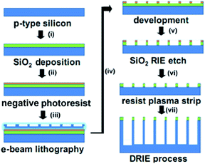
p-Type Si (100) wafers (B-doped, 1–30 Ω cm, LG Siltron) were employed as received. The p-type nature of the wafer was confirmed by Mott–Schottky (M–S) analysis (Fig. S1, ESI†). A 200 nm AlCuSi thin film was sputter-deposited on the unpolished side of a Si wafer which acts as a conducting layer. The fabrication process of SiNW arrays is schematically illustrated in Fig. 1, which involves (i) the deposition of silicon oxide layer (300 nm thick) by plasma-enhanced chemical vapor deposition (CVD), (ii) spin-coating of negative photoresist, (iii) electron-beam lithography, (iv) pattern development, (v) reactive ion etch (RIE) of silicon oxide layer, (vi) plasma strip of photoresist, followed by (vii) a deep RIE process (DRIE). All these processes were conducted in a clean room. It is worth mentioning that all top-down microfabrication techniques used here are well-established in semiconductor industry, and they allow for large-scale fabrication (e.g. over a 8-inch wafer) of vertically-aligned Si NW arrays in a controlled and reproducible manner (Fig. S2, ESI†).Electrode fabrication and characterization
The Si wafer was then cut into small pieces having a dimension of 1.7 × 1.2 cm2 with a patterned area of 0.5 cm2 in the center of each piece, which was subsequently used as a photocathode. The ohmic contact between the sputter-coated AlCuSi layer and Si was achieved by thermally annealing the sample to 400 °C with a ramping rate of 2 °C min−1, maintaining at this temperature for 1 min and cooling down naturally afterwards, all under the protection of high-purity nitrogen (N2, 99.999%) flow. The morphology and microstructure of the samples were examined by scanning electron microscopy (SEM, FEI Quanta FEG 650). The crystal structure of Si photocathodes was studied using X-ray diffractometry (XRD, Panalytical X'Pert PRO) with Cu Kα radiation (λ = 1.540598 Å) and a PIXcel detector.Photoelectrochemical tests
The PEC tests were carried out in a commercially available jacketed photoelectrochemical cell having a quartz window. A graphite rod and a saturated calomel electrode (SCE) were used as counter and reference electrodes, respectively. The Si photocathode was exposed to an electrolyte consisting of 0.5 M sulfuric acid (H2SO4, 95–98%, Sigma-Aldrich) with its back side and non-patterned front side sealed by non-transparent epoxy resin. A solar simulator (LCS-100, Newport) consisting of a 100 W ozone-free xenon lamp with an AM1.5G air mass filter was employed to provide class A – 1 sun illumination (100 mW cm−2) for all PEC tests. The light intensity was calibrated by an optical power meter (Thorlabs GmbH, PM100D) and a thermopile-based power sensor (Thorlabs GmbH, S302C). Linear scan voltammetry (LSV), cyclic voltammetry (CV), electrochemical impedance spectroscopy (EIS) and chronopotentiometry (CP) measurements were carried out using a Zennium electrochemical workstation (Zahner). A scan rate of 10 mV s−1 was used to record LSV and CV curves. The EIS measurements were performed in the frequency range of 10 mHz to 200 kHz at a fixed potential of −0.5 V vs. reversible hydrogen electrode (RHE) under 100 mW cm−2 illumination, with an AC perturbation amplitude of 10 mV. The temperature of the electrolyte was maintained at 23 ± 1 °C during all the tests through a refrigerated chiller (HAAKE Phoenix II, Thermo Scientific). All the potentials were reported versus RHE by converting the potentials measured versus the SCE reference through the following equation:| U(RHE) = U(SCE) + 0.241 + 0.059 × pH | (1) |
Results and discussion
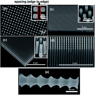
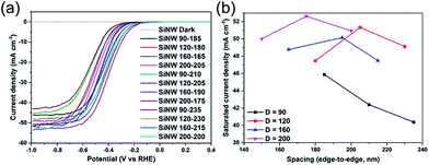
Regular square arrays with different feature sizes ranging from 90 to 200 nm and edge-to-edge inter-wire spacing from 150 to 235 nm were patterned by e-beam lithography on a Si wafer (Fig. S3 and description there, ESI†). Each patterned area has an area of 0.5 cm2. Fig. 2a shows a representative top-view SEM image of the NW array, where each wire has a nominal feature size of 200 nm and a nominal spacing of 175 nm (denoted as “SiNW 200–175” hereafter). It is noted that the etching process led to rounding of the square features, this effect being stronger for NWs with a smaller feature size. Besides, it's found that the actual diameter of SiNWs increases by 25–50 nm in comparison to the nominal one defined in the e-beam writing step, which is typical for the DRIE processes of Si. Fig. 2b–d display side-view SEM images of the NW arrays with the same wire diameter and inter-wire spacing but different lengths of 1, 2 and 5 μm, respectively, where it is seen all NWs are vertically aligned and perpendicular to the Si substrate, and spatially ordered over the entire patterned area. Taking a closer look at the NW surface, it is found that all NWs have wavy side walls (Fig. 2e), which resulted from the alternate passivation and etch steps during the DRIE (i.e., Bosch) process where each “thread” of the NWs corresponds to a “bite” (Fig. S4, ESI†). Similar features were also reported previously for Si microwires (MWs) or NWs fabricated by the top-down lithography approaches.20,21 It's noted that the e-beam lithography and DRIE process did not alter the crystal structure of Si, as evidenced by the identical XRD patterns obtained from the planar Si and SiNW arrays (Fig. S5, ESI†).The influence of NW diameter and inter-wire spacing on the solar-driven HER performance of SiNW photocathodes was first investigated by linear scan voltammetry with the NW length fixed to 1 μm. The SiNW arrays with a diameter of “D” nm and spacing of “S” nm are denoted as “SiNW D–S” in the following. As shown in Fig. 3a, for all NW photocathodes with different D–S combinations, the minimal overpotential (ηsat) needed to reach saturated photocurrent density (Jsat) is around −0.75 V vs. RHE, in agreement with the previous reports.22Fig. 3b summarizes the variation of Jsat derived at −0.75 V vs. RHE as a function of D and S. Jsat varies in the range of 41–52 mA cm−2 as the D–S matrix alters. When D is fixed, Jsat changes with S showing a maxima at an optimal S value. Meanwhile, Jsat is also largely dependent on the NW diameter D. SiNW arrays with D = 90 nm (black data points) exhibit much lower Jsat in comparison to other photocathodes. Notably, all SiNW arrays with D > 100 nm show a Jsat higher than 44 mA cm−2 – the theoretical maximum Jsat of Si predicted according to its band gap. This may indicate that these photocathodes could absorb more light. Similar high Jsat was also observed previously in metal-assisted etching derived SiNW arrays,17 and was ascribed to the enhanced light absorption of SiNWs in the infrared region, which might be associated with the surface states on NWs or sub-band gap absorption induced by impurity states. According to Fig. 3b, the SiNW 200–175 electrode shows the highest Jsat as well as lower overpotential at a given photocurrent density compared to all others. We presume that there is a good compromise from the charge collection efficiency and surface states that renders the 200–175 combination an optimal packing density of SiNWs for efficient PEC hydrogen evolution. Taking this into consideration, we further investigated the effect of NW length on solar-driven HER performance of the SiNW photocathodes while keeping the packing density of NWs to be optimal, namely, 200–175 nm.
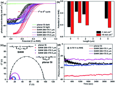
Fig. 4a shows the cyclic voltammograms of SiNW 200–175 arrays with different wire lengths of 1, 2, and 5 μm, recorded in the first 5 cycles. For comparison, CV curves of planar Si were also measured under both dark and illumination conditions. PEC performance of all tested photocathodes gets stabilized after the 5th cycle of cyclic voltammetry, indicating that the Si surface becomes completely wetted by the electrolyte during the first 5 CV scans and a well-defined Si/electrolyte junction is formed. All SiNW arrays show PEC performance better than that of planar Si, with positively shifted onset overpotentials (ηonset, defined as the overpotential at which the cathodic photocurrent density is −1 mA cm−2) of 145–260 mV. This should come from the enlarged electrode/electrolyte contact area and enhanced light absorption of SiNW photocathodes, as repetitively reported before.23,24Fig. 4b compares the ηonset and the overpotential needed to reach the cathodic current density of 10 mA cm−2 (η10) of planar Si and SiNWs with different lengths. ηonset and η10 of the planar Si (i.e. length = 0) are −0.435 and −0.55 V vs. RHE, respectively, substantially negative of those for the 1 μm long SiNW photocathode (ηonset = −0.175 V, η10 = −0.365 V). Interestingly, 1 μm SiNW arrays outperform 2 and 5 μm long ones in terms of both ηonset and Jsat, which may imply that reduced surface recombination and enhanced light absorption occurred in 1 μm long SiNW arrays.
In order to understand the charge transfer kinetics at the Si/electrolyte interface, EIS measurements of both planar Si and SiNW photocathodes were carried out at a potential of −0.5 V vs. RHE under 100 mW cm−2 illumination, and the obtained Nyquist plots are shown in Fig. 4c. The Nyquist plots were fitted with the equivalent circuit models shown in insets of Fig. 4c (Table S1, ESI†), where Rs stands for the equivalent series resistance including the contributions from electrolyte, electrode materials and leads, Q is the constant phase element, W represents the Warburg resistance associated with diffusion, and Rct is the charge transfer resistance. Rct of SiNWs is substantially smaller than that of planar Si, indicating that the NW configuration facilitates electron transfer under PEC hydrogen evolution conditions, in consistence with previous observation for SiNW photoelectrodes.25–27 Interestingly, Rct of 1 μm SiNW is only 7.4 Ω, much smaller than that of 2 and 5 μm long SiNW photocathodes (12.3 and 26.5 Ω, respectively). This agrees well with the CV curves shown in Fig. 4a, and may imply that the number of sharp cuts induced by the DRIE process affects charge transfer rate, given the fact that these three NW samples have the same wire diameter and inter-wire spacing but different lengths (i.e. number of sharp cuts, 15, 30, and 75 for 1, 2 and 5 μm long NWs, respectively).
The stability of both planar Si and SiNW photocathodes was investigated using chronoamperometry at a fixed potential of −0.75 V vs. RHE under 100 mW cm−2 illumination, at which Jsat of each photocathode was obtained. The amplitude of Jsat follows the same trend as that observed in Fig. 4a, namely, JSiNW200–175,1 μm > JSiNW200–175,2 μm > Jplanar Si > JSiNW200–175,5 μm. Remarkably, all Si photocathodes show outstanding catalytic stability for solar-driven hydrogen evolution, and Jsat of SiNW electrodes exhibits very little degradation over time. The slight decrease in Jsat for SiNW photocathodes may result from the formation of a thin silicon oxide layer upon PEC hydrogen evolution.24
In summary, we report the fabrication of highly-ordered, vertically-oriented silicon nanowire arrays using electron-beam lithography followed by deep reactive ion etching of silicon. This top-down approach allows for the large-scale fabrication of silicon nanowire photocathodes with monodisperse diameter and length as well as homogeneous inter-wire spacing, which may help overcome the limitation often dictated by randomly distributed silicon nanowire arrays, namely the PEC performance is limited by poorly performing individual nanowires. We have systematically investigated the influence of structural parameters of silicon nanowires arrays on the photoelectrochemical performance of the electrodes for solar-driven hydrogen evolution, and found that within the range of dimensions under study, silicon nanowires with a diameter of 200 nm, length of 1 μm and inter-wire spacing of 175 nm show the best solar hydrogen evolution performance. It is anticipated that the performance can be further improved with buried p–n junctions and hydrogen evolution catalyst loading. The relevant study is under way.
Conflicts of interest
There are no conflicts to declare.Acknowledgements
This work is funded by ERDF funds through the Portuguese Operational Programme for Competitiveness and Internationalization COMPETE 2020, and National Funds through FCT – The Portuguese Foundation for Science and Technology, under the project “PTDC/CTM-ENE/2349/2014” (Grant Agreement 016660). The work is also partially funded by Portugal-China Bilateral Collaborative Programme (FCT/21102/28/12/2016/S). L. Qiao acknowledges the financial support of the Ministry of Science and Technology of China (2016YFE0132400).Notes and references
- J. A. Turner, Science, 2004, 305, 972–974 CrossRef CAS PubMed.
- S. E. Hosseini and M. A. Wahid, Renewable Sustainable Energy Rev., 2016, 57, 850–866 CrossRef CAS.
- A. Fujishima and K. Honda, Nature, 1972, 238, 37–38 CrossRef CAS PubMed.
- N. Armaroli and V. Balzani, Chem.–Eur. J., 2016, 22, 32–57 CrossRef CAS PubMed.
- K. Sivula and R. van de Krol, Nat. Rev. Mater., 2016, 1, 15010 CrossRef CAS.
- I. Roger, M. A. Shipman and M. D. Symes, Nat. Rev. Chem., 2017, 1, 003 CrossRef CAS.
- K. Sun, S. H. Shen, Y. Q. Liang, P. E. Burrows, S. S. Mao and D. L. Wang, Chem. Rev., 2014, 114, 8662–8719 CrossRef CAS PubMed.
- C. Liu, N. P. Dasgupta and P. D. Yang, Chem. Mater., 2014, 26, 415–422 CrossRef CAS.
- U. Sim, J. Moon, J. Lee, J. An, H. Y. Ahn, D. J. Kim, I. Jo, C. Jeon, S. Han, B. H. Hong and K. T. Nam, ACS Appl. Mater. Interfaces, 2017, 9, 3570–3580 CAS.
- Y. W. Chen, J. D. Prange, S. Duhnen, Y. Park, M. Gunji, C. E. D. Chidsey and P. C. McIntyre, Nat. Mater., 2011, 10, 539–544 CrossRef CAS PubMed.
- X. Q. Bao, M. F. Cerqueira, P. Alpuim and L. F. Liu, Chem. Commun., 2015, 51, 10742–10745 RSC.
- C. R. Cox, M. T. Winkler, J. J. H. Pijpers, T. Buonassisi and D. G. Nocera, Energy Environ. Sci., 2013, 6, 532–538 CAS.
- A. P. Goodey, S. M. Eichfeld, K. K. Lew, J. M. Redwing and T. E. Mallouk, J. Am. Chem. Soc., 2007, 129, 12344–12345 CrossRef CAS PubMed.
- Y. D. Su, C. Liu, S. Brittman, J. Y. Tang, A. Fu, N. Kornienko, Q. Kong and P. D. Yang, Nat. Nanotechnol., 2016, 11, 609–612 CrossRef CAS PubMed.
- U. Sim, J. Moon, J. An, J. H. Kang, S. E. Jerng, J. Moon, S. P. Cho, B. H. Hong and K. T. Nam, Energy Environ. Sci., 2015, 8, 1626 CAS.
- S. Chandrasekaran, T. Nann and N. H. Voelcker, Nano Energy, 2015, 17, 308–322 CrossRef CAS.
- U. Sim, H. Y. Jeong, T. Y. Yang and K. T. Nam, J. Mater. Chem. A, 2013, 1, 5414–5422 CAS.
- G. B. Yuan, H. Z. Zhao, X. H. Liu, Z. S. Hasanali, Y. Zou, A. Levine and D. W. Wang, Angew. Chem., Int. Ed., 2009, 48, 9680–9684 CrossRef CAS PubMed.
- B. C. Zhang, H. Wang, L. He, C. Y. Duan, F. Li, X. M. Ou, B. Q. Sun and X. H. Zhang, Chem. Commun., 2016, 52, 1369–1372 RSC.
- X. Q. Bao, D. Y. Petrovykh, P. Alpuim, D. G. Stroppa, N. Guldris, H. Fonseca, M. Costa, J. Gaspar, C. H. Jin and L. F. Liu, Nano Energy, 2015, 16, 130–142 CrossRef CAS.
- S. K. Choi, W. S. Chae, B. Song, C. H. Cho, J. Choi, D. S. Han, W. Choi and H. Park, J. Mater. Chem. A, 2016, 4, 14008–14016 Search PubMed.
- X. P. Li, Y. J. Xiao, K. Y. Zhou, J. N. Wang, S. L. Schweizer, A. Sprafke, J. H. Lee and R. B. Wehrspohn, Phys. Chem. Chem. Phys., 2015, 17, 800–804 RSC.
- M. D. Kelzenberg, S. W. Boettcher, J. A. Petykiewicz, D. B. Turner-Evans, M. C. Putnam, E. L. Warren, J. M. Spurgeon, R. M. Briggs, N. S. Lewis and H. A. Atwater, Nat. Mater., 2010, 9, 368 CrossRef CAS.
- J. Oh, H. C. Yuan and H. M. Branz, Nat. Nanotechnol., 2012, 7, 743–748 CrossRef CAS PubMed.
- L. F. Liu and X. Q. Bao, Mater. Lett., 2014, 125, 28–31 CrossRef CAS.
- J. Y. Jung, M. J. Choi, K. Zhou, X. P. Li, S. W. Jee, H. D. Um, M. J. Park, K. T. Park, J. H. Bang and J. H. Lee, J. Mater. Chem. A, 2014, 2, 833–842 CAS.
- Q. Li, M. J. Zheng, L. G. Ma, M. Zhong, C. Q. Zhu, B. Zhang, F. Z. Wang, J. N. Song, L. Ma and W. Z. Shen, ACS Appl. Mater. Interfaces, 2016, 8, 22493–22500 CAS.
Footnotes |
| † Electronic supplementary information (ESI) available: Schematic illustration of DRIE process; SEM images showing the morphology of SiNW arrays with different structural parameters. See DOI: 10.1039/c7se00591a |
| ‡ S. M. Thalluri and L. F. Liu conceived the experiments and drafted the initial manuscript. J. Borme, H. Fonseca and J. Gaspar contributed to silicon nanowire fabrication. All co-authors contributed to discussion and analysis of experimental data. |
| This journal is © The Royal Society of Chemistry 2018 |


