Fabrication of a layered nanostructure PEDOT:PSS/SWCNTs composite and its thermoelectric performance
Haijun Song†, Congcong Liu†, Jingkun Xu*, Qinglin Jiang and Hui Shi
Jiangxi Key Laboratory of Organic Chemistry, Jiangxi Science and Technology Normal University, Nanchang 330013, China. E-mail: xujingkun@tsinghua.org.cn; Fax: +86-791-83823320; Tel: +86-791-88537967
First published on 16th September 2013
Abstract
Layered nanostructure PEDOT:PSS/SWCNTs (single-walled carbon nanotubes) composites have been successfully prepared utilizing a method of two-step spin casting. SEM, FTIR and Raman were used to analysis the influence of the carbon nanotubes characteristics on the morphological, spectroscopic, electrical and thermoelectric properties of the composite materials. The layered nanostructure composites showed both improved electrical conductivity and Seebeck coefficient as compared to pure PEDOT:PSS, which could be attributed to the improvement of electron transport and phonon transport because of the bonding disruption of SO3H group with the PSS chains and the use of quantum confinement and interface effects in layered nanostructures. The maximum electrical conductivity and Seebeck coefficient of the composites reached 241 S cm−1 and 38.9 μV K−1, respectively, and the maximum power factor could be up to 21.1 μW m−1 K−2, about 4 orders of magnitude higher than the pure PEDOT:PSS. This study suggests that constructing layered nanostructure organic–inorganic composites might be a novel and effective way for improving the thermoelectric properties of conducting polymers.
1. Introduction
As the world's demand for energy is causing a dramatic rise in social and the serious environmental problems caused by the combustion of fossil fuel, sustainable energy conservation technologies are attracting significant attention. The resource of low-temperature gradients is ubiquitous, it can arise naturally from geothermal, solar energy, residential heating, automotive exhaust, and industrial processes. With such a huge potential, there is also significant interest in finding cost-effective technologies for generating electrical energy from waste heat. Thermoelectric (TE) materials can effectively and directly convert heat to pollution-free electricity from a waste heat source and could therefore be a green option for various energy-harvesting applications ranging from power generation to microprocessor cooling.1–4 Besides, TE generators are light-weight, silent, reliable, and scalable for widely distributed power generation.3 The energy conversion efficiency of TE devices is quantified by the materials' dimensionless figure-of-merit ZT = S2σT/κ, where σ is the electrical conductivity, S is the Seebeck coefficient (also called the thermopower), κ is the thermal conductivity and T is the absolute temperature.Recently, significant improvements on ZT have been achieved in nanostructured inorganics (e.g., superlattices, nanoinclusions, nanocomposites, etc.),5–8 in particular, by phonon scattering to preferentially reduce the thermal conductivity without the loss of power factor,5 and by energy filtering to independently promote the Seebeck coefficient without greatly suppressing electrical conductivity.8 However, the high cost of raw materials and production facilities as well as heavy metal pollution considerations9 and the poor processability9–12 of inorganic TE materials are limiting their wide applications to TE systems.
Studies have shown theoretically and experimentally that the decoupled TE properties between electrical conductivity and Seebeck coefficient and the reduction of the thermal conductivity mentioned above is equally responsible for the improvement of the figure of merit in such nanostructured semiconductor materials.5,13–15 Based on the above researches, organic semiconductor materials have come to the fore front. Conducting polymers (CPs) have attracted considerable attention as important polymer materials since the initial discovery of doped polyacetylene in 1970s.16 A unique feature of conducting polymers as TE material is their intrinsically low thermal conductivity that typically ranges from 0.028 W m−1 K−1 and 0.6 W m−1 K−1,17–20 which is orders of magnitude lower than those of inorganic TE materials such as PbSe and Bi2Te3,21 and this offers them a significant advantage over conventional inorganic TE materials. Additionally, conducting polymers possess some other advantageous features such as low density, low cost, relatively simple synthesis, and easy processing into versatile forms.11
Among numerous CPs, poly(3,4-ethylenedioxythiophene):poly(styrenesulfonate) (PEDOT:PSS) is well known and considered as the most remarkable CP because of its high conductivity, excellent stability, flexible mechanical properties, and transparency.22 The TE investigations for PEDOT:PSS have attracted growing interest since 2008, numerous results were published regarding both as-received PEDOT:PSS and blended composites.23–26 The addition of dielectric solvents such as dimethyl sulfoxide (DMSO) has been widely accepted as an effective approach to greatly increase the electrical conductivity by several orders of magnitude, while the Seebeck coefficient changes very slightly with the concentration of DMSO and keeps at a low level around 14 μV K−1.24 The low Seebeck coefficient has hampered their further use in TE applications.
Carbon nanotubes (CNTs) are renowned for their extraordinary electrical, mechanical and thermal properties. Besides, the holey structural features of CNTs are beneficial for achieving a high ZT. Nevertheless, the high intrinsic thermal conductivity (3000 W m−1 K−1 at room temperature27) has made it irrelevant for TE applications. But recently it has been reported that the thermal conductivity of a packed bed of three-dimensional random networks of CNTs or the CNT/polymer composite is only about 0.2–0.4W m−1 K−1.28–30 This low thermal conductivity accompany the quantum confinement effect of their charge carriers and the size effect of their heat carriers31 make them promising candidates for use as TE materials.
Recently, several studies examining the TE properties of CNT/polymer composites have been reported, including multiwalled carbon nanotube/poly(3-hexylthiophene) (MWCNTs/P3HT),32 single-wall carbon nanotube (SWCNT)/PANI composites,11 CNT/Nafion nanocomposites,33 CNT/PEDOT:PSS nanocomposite (prepared by physical mixing).30 Most of these researches only showed the enhancement of electrical conductivity; while their Seebeck coefficient have not shown significantly change. It is believed that the multilayered structures can reduce the phonon thermal conductivity, due to additional interface scattering.5,34 We expect this system to be able to work quite well as TE elements.
So in this paper, PEDOT:PSS/SWCNTs nanocomposite with a layered nanostructure has been fabricated utilizing a method of two-step spin casting and its TE property also has been analyzed. It is found that the double-layer nanostructure of PEDOT:PSS/SWCNTs composite can effectively improve the Seebeck coefficient and a relatively high electrical conductivity has obtained simultaneously even without the addition of dielectric solvents.
2. Experimental
2.1. Raw materials
PEDOT:PSS aqueous solution (CLEVIOS PH1000) was purchased from H.C. Starck. The concentration of PEDOT:PSS was 1.3% by weight, and the weight ratio of PSS to PEDOT was 2.5. Carbon nanotubes dispersant was purchased from Chengdu Organic Chemicals Co. Ltd., Chinese Academy of Sciences (Chengdu, China). Polystyrene sulfonic acid (PSSA; M.W. = 75![[thin space (1/6-em)]](https://www.rsc.org/images/entities/char_2009.gif) 000, 30% w/v solution in water) was obtained from Alfa Aesar. Dimethyl sulfoxide (DMSO), ethanol and H2SO4 were purchased from Beijing Chemical Plant (Beijing, China). Polyvinyl alcohol was purchased from Tianjin No. 3 Chemical Reagent Factory (Tianjin, China). These materials were used without further purification.
000, 30% w/v solution in water) was obtained from Alfa Aesar. Dimethyl sulfoxide (DMSO), ethanol and H2SO4 were purchased from Beijing Chemical Plant (Beijing, China). Polyvinyl alcohol was purchased from Tianjin No. 3 Chemical Reagent Factory (Tianjin, China). These materials were used without further purification.2.2. Preparation of layered structured PEDOT:PSS/SWCNTs composites
Originally, the glass substrates (2 × 2 cm2) were cleaned for 3 h with a piranha (H2SO4/H2O2, 3/1 v/v) solution and washed successively by ethanol de-ionized water in sequence, and then dried under vacuum 60 °C in a clean chamber. A 200 μL SWCNTs solution (after an ultrasonic treatment of 15 min) was pipetted on the hydrophilic glass surface and spin-coated from 400 to 2000 rpm for 60 s. After being dried for 12 h in a vacuum oven at 60 °C, the PEDOT:PSS (or doped with 5 V% DMSO) solution was spin-coated on the SWCNTs layer at 400 to 2000 rpm for 30 s to produce the two-layered PEDOT:PSS/SWCNTs film (as shown in Fig. 1). Finally, the obtained film was dried for 12 h in a vacuum oven at 60 °C. For the sake of comparison, we also prepared samples of pure single-layered PEDOT:PSS, two-layered PSS/SWCNTs film, PVA/SWCNTs film. The thicknesses of the samples are shown in Table 1. We can see that for pure SWCNTs thin film its thickness is 92.9 nm. After fabrication of the bilayered nanofilm, the thickness can be enhanced to 110–122.4 nm. Besides, the thickness of SWCNTs/PEDOT:PSS (110.6 nm) is quite close to that of SWCNTs/doped PEDOT:PSS (113.8 nm). Therefore, in the bilayered nanofilm, the thickness of PEDOT:PSS layer (or doped PEDOT:PSS layer) is about 20 nm.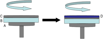 | ||
| Fig. 1 Schematic illustrations of the process in preparation of layered nanostructure: (A) metal tray, (B) glass substrate, (C) SWCNTs nanofilm, (D) PEDOT:PSS nanofilm. | ||
| Sample | CNTs | CNTs/PEDOT:PSS | CNTs/doped PEDOT:PSS | CNTs/PSS | CNTs/PVA |
|---|---|---|---|---|---|
| Thickness (nm) | 92.9 | 110.6 | 113.8 | 122.4 | 117.3 |
2.3. Characterization
The prepared composites were examined by Fourier transform infrared spectroscopy (FTIR, Bruker Vertex 70). The morphology and composition of the composite materials were examined by field emission scanning electron microscopy (FE-SEM) (ZEISS-SIGMA). Raman spectra of the prepared samples were recorded using a MicroRaman spectrometer (LabRam-1B, JY, France) with an excitation length of 633 nm.Electrical conductivity and Seebeck coefficient were measured with a homemade shielded four-point probe apparatus with a Keithley 2700 Multimeter (Cleveland, OH) and a regulated DC power supply (MCH-303D-II, China) in conjunction with Labview (National Instruments, Austin, TX). For electrical conductivity and Seebeck coefficient measurements, samples were cut into pieces of a rectangular shape (length, 20.0 mm; width, 3.0 mm) and suspended by using a thermal paste between two TE devices (typically ∼20 mm apart) used for creating temperature difference. Electrical conductivity was measured by using a current–voltage (IV) sweeping measurement technique with four-point probes after four metal lines were patterned with a silver paint. For the Seebeck coefficient measurement, temperature gradients along the long edge of the sample were measured by two T-type thermocouples. The similar method has been reported by Kim et al.30 Liquid nitrogen was used to provide a low temperature measurement.
3. Results and discussion
Presented in Fig. 2 is the scanning electron microscope (SEM) images of all the samples. In Fig. 2a, for pure PEDOT:PSS, its surface is quite smooth with some grains evenly distribute on the whole films. According to the presently proposed model of the microstructure of conducting PEDOT:PSS, the grains is believed to be PEDOT-rich cores. Fig. 2b clearly shows the network structure of SWCNTs. When SWCNTs film is coated by the pure PEDOT:PSS film, its surface becomes rougher (as shown in Fig. 2c). And from its top view, some tube structure can be seen, indicating the existence of SWCNTs. After doped with DMSO, the top view of the obtained film is much smoother compared to the undoped film (as shown in Fig. 2d). We can hardly see any tube structure from its surface; the reason should be attributed to the conformational change of the PEDOT chains after being doped. Fig. 2e–f are the pictures of sample SWCNTs/PSS and SWCNTs/PVA respectively. Their surfaces are even rougher, also some tube structure can be found.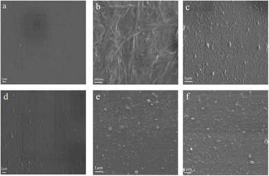 | ||
| Fig. 2 SEM images of the prepared samples: (a) pure PEDOT:PSS nanofilm, (b) pure SWCNTs nanofilm, (c) SWCNTs/PEDOT:PSS layered nanostructure, (d) SWCNTs/PEDOT:PSS (doped with DMSO) layered nanostructure, (e) SWCNTs/PSS layered nanostructure, (f) SWCNTs/PVA layered nanostructure. | ||
The electrical conductivity as a function of temperature for these thin films is shown in Fig. 3. Sample A is pure PEDOT:PSS prepared by spin-coating on the hydrophilic glass at 400 to 2000 rpm for 30 s. The measured electrical conductivity was 0.61 S cm−1 at room temperature. After the preparation of SWCNTs/PEDOT:PSS layered nanostructure, its electrical conductivity raise to 80.8 S cm−1. What's more, the film of SWCNTs/PEDOT:PSS (doped with DMSO) can reach up to 241 S cm−1, which is three orders higher than that of pure PEDOT:PSS. On the other hand, the electrical conductivity of SWCNTs/PSS and SWCNTs/PVA are 46.3 and 30.2 S cm−1, respectively. Due to the ultra-thin nanostructure, the SWCNTs layer and the PSS layer (or PVA layer) can infiltrate into each other. Therefore, the insulate layer of PSS (or PVA) become conductive. Compared with those insulate polymers, conducting polymer PEDOT:PSS can create better electrically connected bridges between tubes. This is a strong indication that electronic properties can be manipulated by altering junctions between nanoparticles. For better TE energy conversion, it is necessary to pass as many electrons as possible across the junctions for high electrical conductivity, while low energy electron transport is deterred at the junctions for a large Seebeck coefficient.
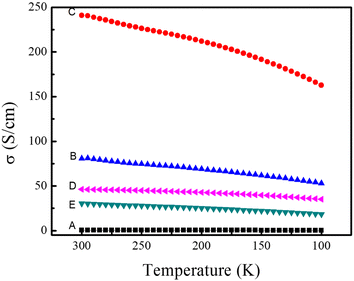 | ||
| Fig. 3 Temperature dependence of the electrical conductivity of the prepared samples: (A) pure PEDOT:PSS nanofilm, (B) SWCNTs/PEDOT:PSS layered nanostructure, (C) SWCNTs/PEDOT:PSS (doped with DMSO) layered nanostructure, (D) SWCNTs/PSS layered nanostructure, (E) SWCNTs/PVA layered nanostructure. | ||
To unveil the mechanism for the conductivity enhancement by the addition of SWCNTs, we have measured FT-IR spectra that provide information about the chemical bonding or molecular structure of the nanocomposite films. As shown in Fig. 4, all the samples have very similar peaks within the wavenumber between 1400 and 1600 cm−1, which originates from the PEDOT:PSS. The absorption peak at 1203 cm−1 of pristine PEDOT:PSS, corresponding to the SO3H group of PSS.35 The addition of CNTs results in a shift of the absorption peak toward the lower wavenumber (from 1203 cm−1 to 1197 cm−1). It is believed that the addition of SWCNTs disrupt the bonding of SO3H group with the insulating PSS chains. In this way, the interaction between the PEDOT and PSS chains is reduced, and the electrical conductivity gets an increase.
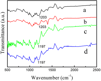 | ||
| Fig. 4 FT-IR spectra of prepared samples: (a) pure PEDOT:PSS, (b) PEDOT:PSS doped with DMSO, (c) SWCNTs/PEDOT:PSS layered nanostructure, (d) SWCNTs/PEDOT:PSS (doped with DMSO) layered nanostructure. | ||
Raman spectra (Fig. 5) provide further evidence of the chemical bonding between PEDOT:PSS and SWCNTs. For the PEDOT:PSS liquid (Fig. 5A), there was a peak at 1436 cm−1, which was assigned to the Cα = Cβ symmetric vibration for the five-member thiophene ring on the PEDOT chains.36,37 After the addition of DMSO, the symmetric Cα = Cβ peak was red-shifted 11 cm−1, as shown in Fig. 5B, which was similar to ethylene glycol (EG)38 and meso-erythritol39 doped PEDOT:PSS. According to the previous reports, the red-shift of Cα = Cβ peak was caused by the thiophene ring of PEDOT:PSS changed from benzoid structure to more conductive quinoid structure.37 Thus, after the change of the PEDOT:PSS structure, the neighboring thiophene rings in the PEDOT chains were almost in the same plane, and the conjugated π-electrons could be delocalized over the whole chain according to Ouyang et al.,39 resulting in more conductive PEDOT. For SWCNT, the G band located at 1581 cm−1, as shown in Fig. 5C. When it is composited with PEDOT:PSS, the peak intensities of PEDOT:PSS decrease or even vanish (Fig. 5D and E), whereas the peaks at 1581 cm−1 dominates. It is believed that the SWCNTs can provide a carrier for PEDOT polymer chains to attach. In this way, the conformation of PEDOT chains changed from coil to expanded-coil or linear conformations, only small part of benzoid structure wasn't transformed into the quinoid structure. So the symmetric vibration of Cα = Cβ becomes much weaker and the corresponding peak at 1436 cm−1 is covered by SWCNTs.
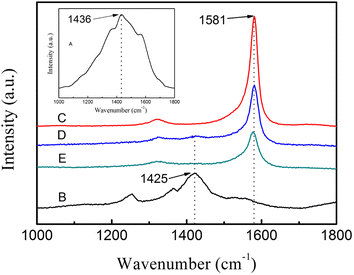 | ||
| Fig. 5 Raman spectra of prepared samples: (A) pure PEDOT:PSS, (B) PEDOT:PSS doped with DMSO, (C) SWCNTs, (D) SWCNTs/PSS layered nanostructure, (E) SWCNTs/PVA layered nanostructure. | ||
Seebeck coefficient is an intrinsic property of materials. It is defined as S = ΔV/ΔT, where ΔV and ΔT are the voltage drops across the material and the temperature gradient along the voltage drop. For most semiconducting polymers, the major parameters of TE transport are strongly correlated and increasing the electrical conductivity will seriously affect the Seebeck coefficient, usually making enhancement of power factor very difficult. However, our approach demonstrated that it is feasible to increase the Seebeck coefficient and electrical conductivity simultaneously so as to achieve a large improvement in power factor (or ZT).
Fig. 6 shows Seebeck coefficient of the samples. All of the films exhibit p-type conduction, indicating the dominant contribution of hole carriers.40 Pure PEDOT:PSS processes a Seebeck coefficient of 15.1 μV K−1, in accordance with the early reports.23,41,42 The preparation of layered nanostructure PEDOT:PSS/SWCNTs has significantly enhanced its Seebeck coefficient. Sample PEDOT:PSS/SWCNTs has got a Seebeck coefficient of 38.9 μV K−1, increased as much as 2.6 times compared to that of pure PEDOT:PSS. This high Seebeck coefficient may be ascribed to the energy filtering effect. In this work, organic–inorganic interfaces were introduced by fabrication of layered nanostructure PEDOT:PSS/SWCNTs composite. The engineered nanoscale interfaces introduce possibilities for both phonon scattering and the energy-dependent scattering of electrical carriers.43–46 By energy filtering, the Seebeck coefficient can be promoted independently without greatly suppressing electrical conductivity. In the bilayered nanofilm, the thickness of PEDOT:PSS layer (about 20 nm), which has already approached nanometer scale, and quantum-confinement effects may arise.47 When a carrier is transported within the network under a temperature gradient, a hopping mechanism for a heterogeneous model may be appropriate.48 On going from one PEDOT:PSS coated SWCNT to another, the carrier would pass through a PEDOT:PSS/SWCNT interface and a PEDOT:PSS layer. In some cases it would hop across a thin air gap. Therefore, lots of nanometer-sized barriers in the form of interfaces would exist on the way. When a large number of carriers hop together mainly in one direction, energy filtering may arise,46,49,50 that is, appropriate potential barriers at crystallite boundaries preferentially allow the carriers with higher energy to pass, thereby increasing the mean carrier energy in the flow, hence, the PEDOT:PSS/SWCNTs bilayered nanofilm received a high Seebeck coefficient of 38.9 μV K−1.
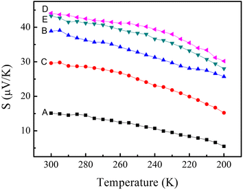 | ||
| Fig. 6 Temperature dependence of the Seebeck coefficient of the prepared samples: (A) pure PEDOT:PSS nanofilm, (B) SWCNTs/PEDOT:PSS layered nanostructure, (C) SWCNTs/PEDOT:PSS (doped with DMSO) layered nanostructure, (D) SWCNTs/PSS layered nanostructure, (E) SWCNTs/PVA layered nanostructure. | ||
Besides, it is worth pointing out that after being doped with DMSO, the Seebeck coefficient of PEDOT:PSS/SWCNTs decreases to 29.6 μV K−1. In general, the Seebeck coefficient is determined by charge diffusion essentially driven by the entropy difference between high- and low-temperature surfaces in internal energy of charge carriers in a TE material. This entropy difference can be changed by electrical and thermal conductivities. When electrical conductivity increases, it can facilitate the charge diffusion between high- and low-temperature surfaces, causing an increase of Seebeck effect. However, increasing electrical conductivity can also lead to an increase in the electron component of thermal conductivity through the Wiedemann–Franz law ((κelectron)/(σT) = C)51 where κelectron is the electron component of thermal conductivity, and C is a constant. This intends to decrease the entropy difference for driving the charge diffusion in the development of Seebeck effect. Therefore, increasing electrical conductivity can cause two competing outcomes: increasing and decreasing the Seebeck effect. It is supposed that after being doped with DMSO, the value of κelectron has increased greatly, which decreases the entropy difference for driving the charge diffusion. Therefore, its Seebeck coefficient becomes lower compared to the undoped film. As mentioned previously, when charge carriers from the TE effect are transported in conducting networks (SWCNTs in this study) within a non-conducting matrix, such as Nafion, PSS or PVA, the Seebeck coefficient of the composites should depend on the Seebeck coefficient of the networked materials.33 In our work, the Seebeck coefficients of layered nanostructure PSS/SWCNTs and PVA/SWCNTs films are 44.1 and 43.3 μV K−1, respectively. Closing to the reported Seebeck coefficient of SWCNTs (42 μV K−1).52
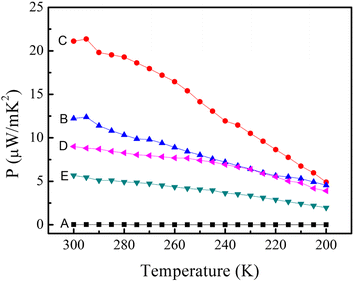
The power factors (S2σ) of pure PEDOT:PSS film and layered nanostructure composites are shown in Fig. 7. The power factors of all the samples decreased slowly with decreasing temperature indicating a semiconductor behavior. The power factor of pure PEDOT:PSS film is 1.4 × 10⁻² μW m−1 K−2. After the preparation of layered nanostructure PEDOT:PSS/SWCNTs, the value can be up to 12.2 μW m−1 K−2. Owing to the improvement of electrical conductivity of the doped PEDOT:PSS, the highest power factor can be up to 21.1 μW m−1 K−2, three orders of magnitude higher than that of pure PEDOT:PSS. This value is much higher than those of some previous publications on the TE performance of CNT/polymer composite, such as PANI/unoxidized SWNT with a power factor of 0.6 μW m−1 K−2,53 CNT/Nafion films with a power factor of 1.0 μW m−1 K−2,33 CNT/PANI nanocomposites with a maximum power factor of 5.0 μW m−1 K−2.54 They are competitive with some good works published, such as SWCNTs/PEDOT:PSS composite TE materials with a highest power factor of 25 μW m−1 K−2 when the content of SWCNTs is 35 wt%,30 PVAc/MWCNTs (stabilized with sodium deoxycholate) with a power factor of 42.8 μW m−1 K−2.55
 | ||
| Fig. 7 Temperature dependence of the power factor of prepared samples: (A) pure PEDOT:PSS nanofilm, (B) SWCNTs/PEDOT:PSS layered nanostructure, (C) SWCNTs/PEDOT:PSS (doped with DMSO) layered nanostructure, (D) SWCNTs/PSS layered nanostructure, (E) SWCNTs/PVA layered nanostructure. | ||
The inherently low κ of conducting polymers provides them a great potential probability of TE application. The high intrinsic thermal conductivity of SWCNTs can be as high as 103 W m−1 K−1 at room temperature.27 However, it has been previously reported that the thermal conductivity of CNT/polymer composites is relatively insensitive to the CNT concentration.11,54 Some recent researches also prove this point, such as PVAc/MWCNTs with a thermal conductivity of 0.17–0.22 W m−1 K−1;56 SWCNTs/PANI nanocomposites with a thermal conductivity of 0.45 W m−1 K−1;54 PEDOT:PSS/SWCNTs composites with a thermal conductivity of 0.2–0.4 W m−1 K−1.29 Previously, our group has reported the thermal conductivity of pure PEDOT:PSS, the measured value was 0.17 W m−1 K−1 at room temperature.23 Because of the difficulty in manipulation of the nanofilm, we have not measured the thermal conductivity. However, it is believed that the construction of layered nanostructure can reduce the thermal conductivity. The thermal conductivity includes both electronic (κe) and phonon (κp) pieces, for semiconductors, the electrical conductivity is low (100–102 S cm−1), and therefore, the proportion of κe to κtotal is very small. The κtotal of the composites mainly depends on the κp. Previous theoretical and experimental investigations have indicated that the nanostructures, including nanoinclusions and nanointerfaces in composites, can scatter phonons and reduce κp.57,58 In this work, organic–inorganic interfaces were created by fabrication of layered nanostructure PEDOT:PSS/SWCNTs composite. Phonon scattering has been introduced by the bilayered interfaces with widths on the order of nms.5,34 In addition, the layered nanostructure can form heterojunctions between PEDOT:PSS layer and SWCNTs layer. These hetero-junctions can be effectively used to lower thermal conductivity by phonon scattering at the interfaces of separate materials due to boundaries and imperfections.59–63 Therefore, theoretically, the thermal conductivity of layered nanostructure PEDOT:PSS/SWCNTs should be kept at a relatively low level that in consistent with most of the conducting polymers.
The value of power factor of the layered nanostructure PEDOT:PSS/SWCNTs composite here is still inferior to those of conventional TE materials. Nevertheless, the enhancement effect is very remarkable. We expect that some TE nanocomposites with high performances could be achieved using a method similar to that suggested here. For instance, by replacing PEDOT:PSS with other conductive polymers such as polyacetylene (PA) or polythiophene (PTh), whose Seebeck coefficient has been reported to be as high as 103 μV K−1.64–66 Further improvement in Seebeck coefficient and electrical conductivity might be achieved by construction of layered nanostructure composites with a low thermal conductivity. Thus, this approach may provide a general strategy for making low-dimensional composites where the quantum-confinement effect may arise, allowing new opportunities to improve S and σ simultaneously to achieve better TE properties.47
4. Conclusions
In summary, we have reported a new approach to enhance TE properties. By preparation of layered nanostructure PEDOT:PSS/SWCNTs composite, remarkably enhanced electrical conductivity and Seebeck coefficient have been obtained due to the disruption of the bonding of SO3H group with the insulating PSS chains and the facilitation of the charge diffusion between high- and low-temperature surfaces after the addition of SWCNTs. The calculated power factor can be as high as 21.1 μW mK−2, which is several orders larger than that of pure PEDOT:PSS. Furthermore, this approach may potentially be extended to other material systems and provide a facile and general strategy for synthesizing TE materials with high performance.Acknowledgements
This work was supported by the National Natural Science Foundation of China (51203070 & 51073074) and Jiangxi Provincial Department of Education (GJJ12595 & GJJ11590 & GJJ13565).References
- G. Chen, M. S. Dresselhaus, G. Dresselhaus, J. P. Fleurial and T. Caillat, Int. Mater. Rev., 2003, 48, 45 CrossRef CAS PubMed.
- T. M. Tritt, H. Boettner and L. Chen, Mater. Res. Bull., 2008, 33, 366 CrossRef CAS.
- G. J. Snyder and E. S. Toberer, Nat. Mater., 2008, 7, 105 CrossRef CAS PubMed.
- L. Mario and N. Ahmed, Nat. Mater., 2011, 10, 409 CrossRef PubMed.
- R. Venkatasubramanian, E. Siivola, T. Colpitts and B. O'Quinn, Nature, 2001, 413, 597 CrossRef CAS PubMed.
- K. F. Hsu, S. Loo, F. Guo, W. Chen, J. S. Dyck, C. Uher, T. Hogan, E. K. Polychroniadis and M. G. Kanatzidis, Science, 2004, 303, 818 CrossRef CAS PubMed.
- W. J. Xie, J. He, H. J. Kang, X. F. Tang, S. Zhu, M. Laver, S. Y. Wang, J. R. D. Copley, C. M. Brown, Q. J. Zhang and T. M. Tritt, Nano Lett., 2010, 10, 3283 CrossRef CAS PubMed.
- S. V. Faleev and F. Leonard, Phys. Rev. B: Condens. Matter Mater. Phys., 2008, 77, 214304 CrossRef.
- J. J. Li, X. F. Tang, H. Li, Y. G. Yan and Q. J. Zhang, Synth. Met., 2010, 160, 1153 CrossRef CAS PubMed.
- F. J. DiSalvo, Science, 1999, 285, 703 CrossRef CAS.
- Q. Yao, L. D. Chen, W. Q. Zhang, S. C. Liufu and X. H. Chen, ACS Nano, 2010, 4, 2445 CrossRef CAS PubMed.
- N. Toshima, Macromol. Symp., 2002, 186, 81 CrossRef CAS.
- J. C. Caylor, K. Coonley, J. Stuart, T. Colpitts and R. Venkatasubramanian, Appl. Phys. Lett., 2005, 87, 023105 CrossRef.
- A. Balandin and K. L. Wang, J. Appl. Phys., 1998, 84, 6149 CrossRef CAS.
- G. Chen, Phys. Rev. B: Condens. Matter Mater. Phys., 1998, 57, 14958 CrossRef CAS.
- H. Shirakawa, E. J. Louis, A. G. MacDiarmid, C. K. Chiang and A. J. Heeger, Chem. Commun., 1977, 578 RSC.
- X. Gao, K. Uehara, D. D. Klug, S. Patchkovskii, J. S. Tse and T. M. Tritt, Phys. Rev. B: Condens. Matter Mater. Phys., 2005, 72, 125202 CrossRef.
- H. Yan, N. Ohno and N. Toshima, Chem. Lett., 2000, 392 CrossRef CAS.
- H. Yan, N. Sada and N. Toshima, J. Therm. Anal. Calorim., 2002, 69, 881 CrossRef CAS.
- P. B. Kaul, K. A. Day and A. R. J. Abramson, J. Appl. Phys., 2007, 101, 083507 CrossRef.
- D. M. Rowe, Thermoelectrics Handbook: Macro to Nano, CRC Press, Boca Raton, FL, 2006, vol. 27 Search PubMed.
- Y. J. Wang, J. Phys.: Conf. Ser., 2009, 152, 012023 CrossRef.
- F. X. Jiang, J. K. Xu, B. Y. Lu, Y. Xie, R. J. Huang and L. F. Li, Chin. Phys. Lett., 2008, 25, 2202 CrossRef CAS.
- K. C. Chang, M. S. Jeng, C. C. Yang, Y. W. Chou, S. K. Wu, M. A. Thomas and Y. C. Peng, J. Electron. Mater., 2009, 38, 1182 CrossRef CAS.
- B. Zhang, J. Sun, H. E. Katz, F. Fang and R. L. Opila, ACS Appl. Mater. Interfaces, 2010, 2, 3170 CAS.
- K. C. See, J. P. Feser, C. E. Chen, A. Majumdar, J. J. Urban and R. A. Segalman, Nano Lett., 2010, 10, 4664 CrossRef CAS PubMed.
- P. Kim, L. Shi, A. Majumdar and P. L. McEuen, Phys. Rev. Lett., 2001, 87, 215502 CrossRef CAS.
- R. S. Prasher, X. J. Hu, Y. Chalopin, N. Mingo, K. Lofgreen, S. Volz, F. Cleri and P. Keblinski, Phys. Rev. Lett., 2009, 102, 105901 CrossRef.
- Y. Choongho, C. Kyungwho, Y. Liang and C. G. Jaime, ACS Nano, 2011, 5, 7885 CrossRef PubMed.
- D. Kim, Y. Kim, K. Choi, J. C. Grunlan and C. H. Yu, ACS Nano, 2010, 4, 513 CrossRef CAS PubMed.
- J. P. Small, L. Shi and P. Kim, Solid State Commun., 2003, 127, 181 CrossRef CAS.
- Y. Du, S. Z. Shen, W. D. Yang, K. F. Cai and P. S. Casey, Synth. Met., 2012, 162, 375 CrossRef CAS PubMed.
- Y. Choi, Y. Kim, S.-G. Park, Y.-G. Kim, B. J. Sung, S.-Y. Jang and W. Kim, Org. Electron., 2011, 12, 2120 CrossRef CAS PubMed.
- L. D. Hicks and M. D. Dresselhaus, Phys. Rev. B: Condens. Matter Mater. Phys., 1993, 47, 12727 CrossRef CAS.
- P. L. Anto, C. Y. Panicker, H. T. Varghese and D. Philip, J. Raman Spectrosc., 2006, 37, 1265 CrossRef CAS.
- S. Garreau, J. L. Duvail and G. Louarn, Synth. Met., 2002, 125, 325 CrossRef CAS.
- M. Lapkowski and A. Pron, Synth. Met., 2000, 110, 79 CrossRef CAS.
- J. Ouyang, Q. F. Xu, C. W. Chu, Y. Yang, G. Li and J. Shinar, Polymer, 2004, 45, 8443 CrossRef CAS PubMed.
- J. Ouyang, C. W. Chu, F. C. Chen, Q. F. Xu and Y. Yang, Adv. Funct. Mater., 2005, 15, 203 CrossRef CAS.
- S. C. K. Misra and S. Chandra, Indian J. Chem., 1994, 33, 583 Search PubMed.
- M. Scholdt, H. Do, J. Lang, A. Gall, A. Colsmann, U. Lemmer, J. D. Koenig, M. Winkler and H. Boettner, J. Electron. Mater., 2010, 39, 1589 CrossRef CAS PubMed.
- C. C. Liu, F. X. Jiang, M. Y. Huang, R. R. Yue, B. Y. Lu, J. K. Xu and G. D. Liu, J. Electron. Mater., 2011, 40, 648 CrossRef CAS PubMed.
- W. Kim, J. Zide, A. Gossard, D. Klenov, S. Stemmer, A. Shakouri and A. Majumdar, Phys. Rev. Lett., 2006, 96, 4 Search PubMed.
- K. Ahn, M. K. Han, J. Q. He, J. Androulakis, S. Ballikaya, C. Uher, V. P. Dravid and M. G. Kanatzidis, J. Am. Chem. Soc., 2010, 132, 5227 CrossRef CAS PubMed.
- D. Vashaee and A. Shakouri, Phys. Rev. Lett., 2004, 92, 106103 CrossRef.
- T. E. Humphrey, M. F. O. Dwyer and H. Linke, J. Phys. D: Appl. Phys., 2005, 38, 2051 CrossRef CAS.
- M. S. Dresselhaus, G. Chen, M. Y. Tang, R. G. Yang, H. Lee, D. Z. Wang, Z. F. Ren, J. P. Fleurial and P. Gogna, Adv. Mater., 2007, 19, 1043 CrossRef CAS.
- A. B. Kaiser, Phys. Rev. B: Condens. Matter Mater. Phys., 1989, 40, 2806 CrossRef.
- B. Y. Moizhes and V. A. Nemchinsky, in Proc. 11th Int. Conf. on Thermo-electrics, ed. K. R. Rao, University of Texas Press, Arlington, TX, 1992, pp. 232–235 Search PubMed.
- Y. I. Ravich, in CRC Handbook of Thermoelectrics, ed. D. M. Rowe, CRC Press, Boca Raton, FL, 1995, pp. 67–73 Search PubMed.
- P. Cotterill and P. R. Mould, Recrystallization and Grain Growth in Metals, John Wiley & Sons, New York, 1976, vol. 150 Search PubMed.
- C. H. Yu, L. Shi, Z. Yao, D. Y. Li and A. Majumdar, Nano Lett., 2005, 5, 1842 CrossRef CAS PubMed.
- R. C. Y. King, F. Roussel, J. F. Brun and C. Gors, Synth. Met., 2012, 162, 1348 CrossRef CAS PubMed.
- C. Z. Meng, C. H. Liu and S. S. Fan, Adv. Mater., 2010, 22, 535 CrossRef CAS PubMed.
- G. P. Moriarty, J. N. Wheeler, C. Yu and J. C. Grunlan, Carbon, 2012, 50, 885 CrossRef CAS PubMed.
- P. M. Gregory, N. W. Jamie, Y. Choongho and C. G. Jaime, Carbon, 2012, 50, 885 CrossRef PubMed.
- A. J. Minnich, M. S. Dresselhaus, Z. F. Ren and G. Chen, Energy Environ. Sci., 2009, 2, 466 CAS.
- J. R. Sootsman, H. Kong, C. Uher, J. J. D'Angelo, C. I. Wu, T. P. Hogan, T. Caillat and M. G. Kanatzidis, Angew. Chem., Int. Ed., 2008, 47, 1 CrossRef PubMed.
- B. S. W. Kuo, J. C. M. Li and A. W. Schmid, Appl. Phys. A, 1992, 55, 289 CrossRef.
- M. Asheghi, Y. K. Leung, S. S. Wong and K. E. Goodson, Appl. Phys. Lett., 1997, 71, 1798 CrossRef CAS.
- P. Reddy, S. Jang, R. Segalman and A. Majumdar, Science, 2007, 315, 1568 CrossRef CAS PubMed.
- R. Huang, R. Ram, M. Manfra, M. Connors, L. Missaggia and G. Turner, J. Appl. Phys., 2007, 101, 046102 CrossRef.
- J. Malen, S. Yee, A. Majumdar and R. Segalman, Chem. Phys. Lett., 2010, 491, 109 CrossRef CAS PubMed.
- J. R. Reynolds, J. B. Schlenoff and J. C. W. Chien, J. Electrochem. Soc., 1985, 132, 1131 CrossRef CAS PubMed.
- S. Hayashi, K. Kaneto, K. Yoshino, R. Matsushita and T. Matsuyama, J. Phys. Soc. Jpn., 1986, 55, 1971 CrossRef CAS.
- E. Pinter, Z. A. Fekete, O. Berkesi, P. Makra, A. Patzko and C. Visy, J. Phys. Chem. C, 2007, 111, 11872 CAS.
Footnote |
| † The authors contributed equally to this work. |
| This journal is © The Royal Society of Chemistry 2013 |