 Open Access Article
Achieving pure room temperature phosphorescence (RTP) in phenoselenazine-based organic emitters through synergism among heavy atom effect, enhanced n → π* transitions and magnified electron coupling by the A–D–A molecular configuration†
Daokun
Zhong
,
Siqi
Liu
,
Ling
Yue
 ,
Zhao
Feng
,
Hongyan
Wang
,
Peng
Yang
,
Bochao
Su
,
Zhao
Feng
,
Hongyan
Wang
,
Peng
Yang
,
Bochao
Su
 ,
Xiaolong
Yang
 ,
Yuanhui
Sun
 and
Guijiang
Zhou
 *
*
Engineering Research Center of Energy Storage Materials and Devices, School of Chemistry, State Key Laboratory for Mechanical Behavior of Materials, Xi'an Jiaotong University, Xi'an 710049, P. R. China. E-mail: zhougj@mail.xjtu.edu.cn
First published on 2nd May 2024
Abstract
The weak spin–orbit coupling (SOC) in metal-free organic molecules poses a challenge in achieving phosphorescence emission. To attain pure phosphorescence in RTP organic emitters, a promising molecular design concept has been proposed. This involves incorporating n → π* transitions and leveraging the heavy atomic effect within the spin–orbit charge transfer-induced intersystem crossing (SOCT-ISC) mechanism of bipolar molecules. Following this design concept, two bipolar metal-free organic molecules (PhSeB and PhSeDB) with donor–acceptor (D–A) and acceptor–donor–acceptor (A–D–A) configurations have been synthesized. When the molecular configuration changes from D–A to A–D–A, PhSeDB exhibits stronger electron coupling and n → π* transitions, which can further enhance the spin–orbit coupling (SOC) together with the heave atom effect from the selenium atom. By the advanced synergism among enhanced n → π* transitions, heavy atom effect and magnified electron coupling to efficiently promote phosphorescence emission, PhSeDB can achieve pure RTP emission in both the solution and doped solid film. Thanks to the higher spin–orbit coupling matrix elements (SOCMEs) for T1 ↔ S0, PhSeDB attains the highest phosphorescence quantum yield (ca. 0.78) among all the RTP organic emitters reported. Consequently, the purely organic phosphorescent light-emitting diodes (POPLEDs) based on PhSeDB achieve the highest external quantum efficiencies of 18.2% and luminance of 3000 cd m−2. These encouraging results underscore the significant potential of this innovative molecular design concept for highly efficient POPLEDs.
Introduction
Although phosphorescent emitters based on precious metals have been successfully commercialized, their applications still face great challenges, such as high production costs and stability issues.1 In response to these challenges, there has been a notable focus on the development of pure organic emitters with room temperature phosphorescence (RTP) without precious metals.2 These alternatives aim to achieve efficient intersystem crossing (ISC) and hence bring efficient phosphorescence emission at room temperature. However, identifying a molecular design capable of facilitating efficient decay from the triplet excited state (Tn) to the ground state (S0) through strong spin–orbit coupling (SOC) remains a challenging task.3Several strategies have been explored to induce efficient phosphorescence from purely organic molecules, such as leveraging n → π* transitions and the heavy-atom effect, which can promote a strong spin–orbit coupling (SOC) process.4 For instance, Jin et al. reported the use of 1,3,5-trifluoro-2,4,6-triiodobenzene (TITFB) as a simple RTP material, demonstrating its potential in promoting n → π* transitions.5 However, TITFB exhibited weak phosphorescence, limiting its applicability in OLED devices. Other studies, like that done by Huang et al., have focused on designing organic phosphors with ultralong phosphorescence features, emphasizing the role of the heavy-atom effect in facilitating SOC to promote an efficient intersystem crossing (ISC) process.6 Despite these advancements, many RTP materials with n → π* transitions or heavy atoms like Br and I are not practical for OLED devices due to their efficient phosphorescence only occurring in the crystalline state or rigid matrices.7 Despite that several sulfur-based RTP emitters have been reported,8 they just exhibit low phosphorescence quantum yield as a result of the inefficient SOC caused by the weak heavy-atom effect induced by the sulfur atom. To address this, the heavier selenium atom has been explored to construct RTP emitters, showing higher photoluminescence quantum yields (PLQY) and enhanced external quantum efficiency (EQE) in OLEDs.1c,9 For example, Lee et al. designed and synthesized a PSe3Cz phosphor with a phenoselenazine core for triggering phosphorescence and a secondary chromophore for improved PLQY.10 Then, the PSe3Cz emitter achieved a high PLQY of 50.2% and EQE of 13.2% in organic phosphorescent light-emitting diodes (POPLEDs). However, PSe3Cz still exhibits fluorescence emission in its PL spectra. In addition, they also reported a metal-free molecule PSeBz,11 which has both the thermally activated delayed fluorescence emission (TADF) and phosphorescence features. Obviously, highly efficient RTP emission still cannot be achieved just by the incorporation of the selenium atom into organic skeletons. So, new molecular design conception should be definitely developed to enhance the phosphorescence efficiency of RTP emitters.
Recently, the strategic design of bipolar organic molecules has leveraged the spin–orbit charge transfer-induced intersystem crossing (SOCT-ISC) mechanism to achieve a heightened quantum yield for the triplet excited state, while avoiding the incorporation of heavy atoms.12 This phenomenon parallels the characteristics of the n → π* transition, wherein electron coupling (entailing charge separation or recombination) induces a change in molecular orbital angular momentum, thereby generating a magnetic torque conducive to electron spin flipping or rephrasing and hence enhancing the ISC process.13 Unfortunately, organic molecules relying on the SOCT-ISC mechanism possess prolonged triplet excited state lifetimes and diminished luminescence efficiency, disfavoring their application in developing efficient emitters for OLEDs. However, the insights gained from this mechanism continue to guide the design and synthesis of efficient RTP materials.
To address the need for highly efficient RTP emitters, this paper introduces a new approach by incorporating enhanced n → π* transitions and the heavy atom effect into the SOCT-ISC system. This aims to promote SOC via synergism among heavy atom effect, enhanced n → π* transitions and magnified electron coupling and hence achieve highly efficient phosphorescence at room temperature. Based on this new molecular design, two phenoselenazine-based bipolar organic molecules (PhSeB and PhSeDB) with donor–acceptor (D–A) and acceptor–donor–acceptor (A–D–A) configurations have been obtained. For PhSeDB with the A–D–A configuration, both N and Se atoms in the phenoselenazine donor can contribute lone pair electrons (n electrons) to enhance n → π* transitions with the empty pπ* orbitals in the two –B(Mes)2 acceptors. At the same time, the two –B(Mes)2 acceptors in PhSeDB will accelerate and magnify the electron coupling with respect to the analog PhSeB with a single –B(Mes)2 acceptor. By the advanced synergism to promote phosphorescence emission, PhSeDB can achieve pure RTP emission in both the solution and doped solid film at 298 K. Critically, PhSeDB adopting the D–A–D configuration exhibits higher spin–orbit coupling matrix elements (SOCMEs) for T1 ↔ S0 than the D–A type PhSeB, resulting in the highest phosphorescence quantum yield (ca. 0.78). Furthermore, PhSeDB can show very impressive EL performance in OLEDs with an EQE of 18.2% and luminance of 3000 cd m−2, representing the state-of-the-art EL data ever achieved by RTP emitters. Definitely, these encouraging results demonstrate the effectiveness of the proposed molecular design mechanism for developing highly efficient RTP emitters.
Results and discussion
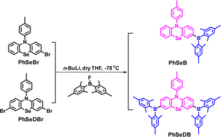
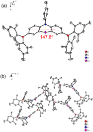
The synthetic strategies for both intermediate and target compounds are outlined in Schemes 1 and S1,† with detailed synthetic procedures provided in the ESI.† The chemical structures of PhSeB and PhSeDB are characterized using 1H and 13C NMR. Furthermore, the solid-state structure of PhSeDB is fully characterized by single crystal X-ray crystallographic analysis (Fig. 1 and Table S1 in the ESI†). Notably, owing to the large diameter of the Se atom, the peripheral benzene rings adopt a folded configuration, deviating from the plane with a dihedral angle of 147.8° (Fig. 1a). This folded arrangement prevents the formation of severe co-planar packing, effectively mitigating the (ACQ) effect typically observed in the polycyclic π-conjugated materials.14 The absence of π⋯π interactions in the crystal structure of PhSeDB further confirms this prevention of severe aggregation (Fig. 1b).Thermal properties and photophysical characterization
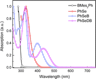
The thermal properties of PhSeB and PhSeDB are investigated through thermogravimetric analysis (TGA) under a nitrogen flow. TGA results reveal their thermal stability, with decomposition temperatures at 347 and 316 °C, respectively (Fig. S1†). The good thermal stability of PhSeB and PhSeDB ensures stability during the fabrication and operation of the respective electroluminescent (EL) devices.UV-vis absorption spectra in CH2Cl2 solutions of PhSeB and PhSeDB are illustrated in Fig. 2. For comparison, the absorption behaviors of the electron donor (D, PhSe) and electron acceptor dimesityl(phenyl)borane (A, BMes2Ph) are also examined in CH2Cl2 (Fig. 2). In both PhSeB and PhSeDB, absorption bands are around 300–400 nm, which are similar to those of pristine PhSe, indicating their origin from the electron transition in their phenoselenazine donor. Additionally, in comparison with D and A, PhSeB and PhSeDB exhibit distinct low-energy absorption bands around 350–490 nm and 387–530 nm, respectively. These bands can be attributed to the charge transfer (CT) transitions owing to the strong electron coupling between D and A groups in PhSeB and PhSeDB.15 This suggests that these bipolar molecules can rapidly achieve charge separation or recombination under excitation, facilitating rapid spin–orbit coupling (SOC) and generation of triplet excited states. Moreover, in comparison to D–A type PhSeB, PhSeDB with the A–D–A configuration displays a red-shifted absorption curve, indicating its stronger electron coupling effect.13a,16 Therefore, it is easier for PhSeDB to achieve charge separation or recombination compared with PhSeB. Compared to the traditional SOCT-ISC systems with the D–A configuration, it seems that the A–D–A structure can show advantage in magnifying the electron coupling effect to favor the SOC effect and triplet excited state generation.
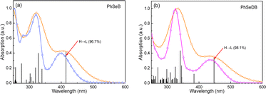
To directly interpret the absorption behavior of PhSeB and PhSeDB, simulated UV-vis spectroscopy (Fig. 3) with discrete vertical transitions and time-dependent density functional theory (TD-DFT) calculations (Fig. 4) have been conducted. The results in Fig. 3 clearly show that the CT absorption bands in PhSeB and PhSeDB are mainly contributed by the transition from the highest occupied molecular orbital (HOMO) to the lowest unoccupied molecular orbital (LUMO) (H → L transition). Based on the distribution pattern of the front molecular orbitals (FMOs) in Fig. 4, H → L transitions in PhSeB and PhSeDB exhibit dominant n → π* features from n electrons on N and Se atoms to the pπ* orbitals of the B atom in the –B(Mes)2 acceptors. Hence, the electron coupling in PhSeB and PhSeDB is induced by their n → π* transitions. Differently, through checking the contribution from both N and Se atoms to the HOMO and LUMO of PhSeB and PhSeDB, it is found that the n → π* transition in PhSeDB is contributed by both N and Se atoms, while only the Se atom contributes this transition in PhSeB. So, PhSeDB with the A–D–A configuration possesses more enhanced n → π* transitions than the D–A type PhSeB. This outcome is supported by the red-shifted CT absorption band of PhSeDB with respect to that of PhSeDB in Fig. 2.
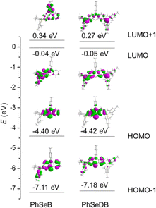 | ||
| Fig. 4 Molecular orbital patterns (isocontour value = 0.025) for PhSeB and PhSeDB based on their optimized S0 geometries. | ||
Photoluminescence (PL) spectra for PhSeB and PhSeDB are recorded in CH2Cl2 at both 298 K and 77 K. In Fig. 5a, the emission peaks for PhSeB and PhSeDB in CH2Cl2 at 298 K are observed at 522 nm and 536 nm. The lifetimes for their emission bands at 298 K are 534.3 μs for PhSeB and 487.6 μs for PhSeDB in solution under a nitrogen atmosphere (Fig. S2†), respectively. The long lifetime in the order of illustrates that their emission should correspond to triplet states. At 77 K, the PL spectrum for PhSeB exhibits two distinct emission bands at 491 nm and 552 nm, while PhSeDB emits just one dominate emission band at 520 nm with a weaker shoulder around 580 nm (Fig. 5a). Surely, different emissive excited sates concerning triplet states are involved in PhSeB and PhSeDB.
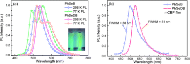 | ||
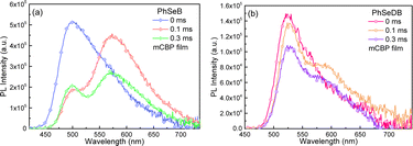
| Fig. 5 PL spectra of PhSeB and PhSeDB, (a) measured in CH2Cl2 solution at 298 and 77 K and (b) measured in mCBP films at 298 K. | ||
With the aim to clarify their emission behavior, the photophysical properties of PhSeB and PhSeDB doped in mCBP films have been investigated (Fig. 5b, 6, and 7). According to the spectral line patterns of the PL spectra at different delay times, PhSeB shows two distinct two emission bands at ca. 513 nm and 580 nm, respectively (Fig. 6a). The variation of relative intensity between the two emission bands at different delay times indicates that the emission band at ca. 513 nm shows a shorter lifetime than that at ca. 580 nm (Fig. 6a). So, it can be concluded that the two emission bands of PhSeB should be induced by different mechanisms. In contrast, PhSeDB exhibits a nearly identical spectral line-shape for the PL spectra at different delay times (Fig. 6b), showing a singlet emission mechanism.
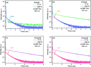 | ||
| Fig. 7 The transient PL decay data under nitrogen for PhSeB and PhSeDB measured in mCBP films. (a) at 500 nm and (b) at 570 nm for PhSeB; (c) at 530 nm and (d) at 580 nm for PhSeDB. | ||
In order to show their different emission mechanisms, transient PL decay curves have been measured at 77 K and 298 K under nitrogen (Fig. 7). For the emission band at ca. 500 nm for PhSeB, its intensity is weakened with lowing temperature (Fig. 7a), exhibiting typical TADF features due to the restrained reverse inter-system crossing (RISC) process from triplet states (T1) to singlet states (S1) at low temperature.11,17 Differently, the intensity of the emission band at ca. 570 nm for PhSeB is enhanced with lowing temperature (Fig. 7b), showing a typical phosphorescence character owing to the blocking of the thermal quenching process. Hence, the emission from PhSeB consists of both TADF and phosphorescence. However, for PhSeDB, the emission intensities at both 520 nm and 580 nm are simultaneously enhanced with lowing temperature (Fig. 7c and d), representing phosphorescence emission. Due to its very similar lifetime to that associated with 520 nm, the shoulder phosphorescent band at 580 nm should be induced by the vibronic transitions. So, PhSeDB achieves the ability of emitting pure RTP emission. All these results indicate clearly the advantage of the A–D–A configuration associated with PhSeDB in achieving highly efficient RTP with respect to the D–A configuration of PhSeB.
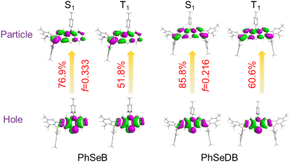
According to their natural transition orbital (NTO) patterns based on both the S1 and T1 optimized geometries (Fig. 8), their hole orbitals of both S1 and T1 states are localized on the n orbitals from N and Se atoms and the π orbitals of the benzene units in the central electron donor, while the particle orbitals consist of both the π* orbitals of the benzene units in the central electron donor and pπ* orbital of the B atoms in the –B(Mes)2 electron acceptors (Fig. 8). Hence, their hole → particle transitions exhibit obvious n → π* transition features. As depicted in Fig. 8, the charge transfer from hole to particle orbitals for PhSeDB with an A–D–A configuration involves the n → π* transition from the n electrons on both N and Se atoms to the π* and pπ* orbitals (Fig. 8), contributing to an enhanced SOC effect according to El-Sayed rules. In contrast, PhSeB with a D–A configuration only exhibits the n → π* transition from the Se atom in the electron donor (Fig. 8). Additionally, the contribution ratio of S0 → T1 excitation to the hole → particle transition associated with the T1 state for PhSeDB is ca. 60.6%, higher than that of PhSeB (ca. 51.8%). These results confirm that PhSeDB should exhibit a superior RTP characteristic compared with PhSeB. Moreover, according to their chemical structure, the proportion of selenium in the PhSeDB molecule is lower than in PhSeB. Thus, the heavy-atom effect in PhSeDB should be weaker than that in PhSeB. Consequently, it would be expected that the RTP characteristics of PhSeB should be stronger than that of PhSeDB. However, experimental results indicate a reverse trend, which can be attributed to the A–D–A molecular configuration of PhSeDB. Compared with PhSeB, PhSeDB possesses two –B(Mes)2 groups as electron acceptors, which can enhance the contributions of n electrons on the N atom to the π* and pπ* orbitals. This leads to heightened n → π* transitions in PhSeDB, thereby enhancing electronic coupling and facilitating RTP emission.
To gauge the SOC effect in PhSeB and PhSeDB, the spin–orbit coupling matrix elements (SOCMEs) between the excited states of different multiples are calculated. As depicted in Fig. 9, PhSeB possesses a moderate SOCME of 5.03 cm−1 for T1 ↔ S0 together with a high f value of 0.333 for fluorescence emission (Fig. 8), demonstrating a favorable thermally activated delayed fluorescence (TADF) channel. This is also accompanied by a facilitated phosphorescent radiation channel owing to a relatively large SOCME. Therefore, PhSeB is expected to achieve effective TADF and RTP emissions simultaneously, aligning with the experimental results. In contrast, the SOCMEs between singlet states and triplet states for PhSeDB are 6.16 cm−1 for S1 ↔ T3, 2.28 cm−1 for S1 ↔ T2, and 0.41 cm−1 for S1 ↔ T1 (Fig. 9), surpassing those of PhSeB. This indicates that singlet excitons for PhSeDB are more readily converted to triplet states through efficient intersystem crossing (ISC). Importantly, PhSeDB exhibits a substantially higher SOCME of 12.75 cm−1 for T1 ↔ S0 (Fig. 9). Consequently, with the greatly reduced fluorescence component due to a smaller f value of 0.216 (Fig. 8), the cooperative effect of both the effective ISC process and efficient phosphorescent radiative processes contributes to the pure RTP emission in PhSeDB.
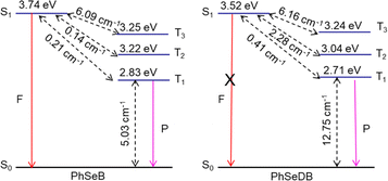 | ||
Fig. 9 Spin–orbit coupling matrix elements (SOCMEs) for PhSeB and PhSeDB with energetic levels of excited states. SOC elements are calculated from  . F = fluorescence; P = phosphorescence. . F = fluorescence; P = phosphorescence. | ||
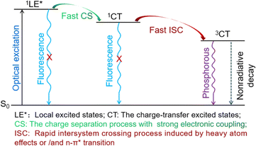
The transition mechanism of PhSeDB, characterized by the pure RTP emission, emerges from a combination of experimental observations and theoretical calculations, as depicted in Fig. 10. Upon optical excitation, PhSeDB promptly forms localized excited states (1LE*). Subsequently, facilitated by the magnified electronic coupling effect induced by the A–D–A configuration, rapid charge separation (CS) occurs,18 leading to the formation of the charge transfer singlet state (1CT) and effectively restraining fluorescence emission from the decay of the 1LE* states (Fig. 10). Then, the presence of the enhanced n → π* transition character together with the heavy atom effect induces efficient intersystem crossing (ISC) through an effective SOC effect, transforming the 1CT states into the charge transfer triplet state (3CT) and effectively suppressing fluorescence emission from the decay of the 1CT states (Fig. 10). Finally, the 3CT states undergo a radiation decay process, culminating in the manifestation of pure RTP emission free of the fluorescent component (Fig. 10). Based on the existence of obvious fluorescent bands in the reported phenoselenazine-based RTP emitters with or without D–A configuration,1c,10,11 the distinctive RTP characteristics associated with PhSeDB should dominantly benefit from the A–D–A configuration which involves advanced synergism among enhanced n → π* transitions, heavy atom effect and magnified electron coupling to promote the SOC effect and hence induce pure RTP emission. However, without n → π* transitions and the heavy atom effect, the traditional SOCT-ISC systems typically just exhibit the electron coupling effect leading to low RTP ability. In addition, it should be noted that the fast CS and ISC processes furnish a relatively short lifetime to the pure RTP emission from PhSeDB, favoring its application in OLEDs.
Despite the CT features, the PL spectra of PhSeB and PhSeDB in CH2Cl2 still exhibit narrow spectral lines with FWHMs of 70 nm and 65 nm, respectively (Fig. 5a). Compared with that of PhSeB, the narrower FWHM in PhSeDB can be ascribed to its shorter-range charge transfer according to the hole → particle transition patterns in Fig. 8. Furthermore, they show even narrower PL spectra in the doped mCBP film with FWHM at 58 nm and 51 nm, respectively (Fig. 5b). Their small FWHM can be ascribed to the short-range charge transfer induced by the –B(Mes)2 electron acceptor, which will shorten the distance of charge transfer and form excited states with more localized features. Furthermore, the short-range charge transfer can facilitate a significant overlap between their HOMO and LUMO, inhibiting non-radiative decays. Examining the FMOs (Fig. 4) reveals p-π conjugation between the empty p orbital on the boron center and the π orbital of the attached phenyl ring. This configuration affords a double bond-like feature of the B–C bonds in PhSeDB and PhSeB, restraining the rotation of the –B(Mes)2 moiety. Additionally, the presence of two methyl groups on the ortho-positions of the carbon atom attached to boron blocks the free rotation of the two mesitylene (Mes) units. Consequently, the –B(Mes)2 moiety cannot effectively quench the radiative triplet excited states of PhSeDB and PhSeB. As a result, high photoluminescence quantum yields (PLQYs) for PhSeB and PhSeDB in doped films are measured to be 0.67 and 0.78, respectively. Additionally, their short PL lifetimes at room temperature in the doped film (Table S2†) contribute to their high PLQYs. Notably, PhSeDB has the highest PLQY reported in the literature for pure RTP materials (Fig. S3 and Table S2†). The high PLQYs will definitely favor their electroluminescent (EL) performances.
Electroluminescent properties
Considering the 1![[thin space (1/6-em)]](https://www.rsc.org/images/entities/char_2009.gif) :
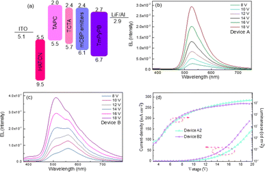
:![[thin space (1/6-em)]](https://www.rsc.org/images/entities/char_2009.gif) 3 singlet–triplet spin statistic ratios under electrical excitation, the high PLQY of PhSeDB and PhSeB emitters paves the way for the development of high-efficiency purely organic room temperature phosphorescent light-emitting diodes (POPLEDs). The electroluminescent (EL) performances utilizing PhSeB and PhSeDB as emitters are comprehensively presented in Table 1, Fig. 11, and 12. The basic device architecture involves indium tin oxide (ITO)/2,3,6,7,10,11-hexacyano-1,4,5,8,9,12-hexaazatriphenylene (HAT-CN, 10 nm)/4,4ʹ-(cyclohexane-1,1-diyl)bis(N,N-di-p-tolylaniline) (TAPC, 40 nm)/4,4′,4′′-tris(carbazole-9-yl)-triphenylamine (TCTA, 5 nm)/3,3′-di(9H-carbazol-9-yl)biphenyl (mCBP:x, 20 nm)/3,3ʹ-[5ʹ-[3-(3-pyridinyl)phenyl][1,1ʹ:3ʹ,1′′-terphenyl]-3,3′′-diyl]bispyridine (TmPyPB, 45 nm)/lithium fluoride (LiF, 1 nm)/aluminum (Al, 100 nm). The corresponding energy-level diagram, device structure, and materials used are illustrated in Fig. 11a and S4.† The current density–voltage–luminance (J–V–L) curves and the efficiency–luminance relationship of the devices are presented in Fig. 11d and 12, respectively, with additional EL results provided in Fig. S5–S7.† The EL profiles (Fig. 11b) for PhSeDB closely resemble the PL profiles in mCBP films, indicating analogous transition contributions. The EL profiles of PhSeDB-based devices are attributed to RTP emission. Notably, significantly distinct voltage-dependent EL spectra are observed for the PhSeB-based devices. At a low voltage (≤12.0 V), PhSeB exhibits a dominant emission peaking at 560 nm, accompanied by a distinguishable shoulder peak at 510 nm (Fig. 11c). The primary emission aligns well with that observed under optical excitation. Similar to PL in the mCBP film, the dominant profile at 560 nm is attributed to the RTP EL emission, while the shoulder peak at 510 nm can be ascribed to an EL band from the TADF mechanism. At high voltage, the decreased peak intensity at 560 nm further confirms the RTP emission character, possibly due to the increased concentration quenching of the long-lived triplet excitons (triplet–triplet annihilation, TTA).19 As discussed earlier regarding PL characteristics in mCBP films, the divergent EL properties of PhSeB-based devices compared to those of the PhSeDB-based devices can be attributed to weaker electronic coupling and n → π* transitions. Therefore, strong electronic coupling emerges as a prerequisite for achieving pure RTP emission during the electroluminescence process.
3 singlet–triplet spin statistic ratios under electrical excitation, the high PLQY of PhSeDB and PhSeB emitters paves the way for the development of high-efficiency purely organic room temperature phosphorescent light-emitting diodes (POPLEDs). The electroluminescent (EL) performances utilizing PhSeB and PhSeDB as emitters are comprehensively presented in Table 1, Fig. 11, and 12. The basic device architecture involves indium tin oxide (ITO)/2,3,6,7,10,11-hexacyano-1,4,5,8,9,12-hexaazatriphenylene (HAT-CN, 10 nm)/4,4ʹ-(cyclohexane-1,1-diyl)bis(N,N-di-p-tolylaniline) (TAPC, 40 nm)/4,4′,4′′-tris(carbazole-9-yl)-triphenylamine (TCTA, 5 nm)/3,3′-di(9H-carbazol-9-yl)biphenyl (mCBP:x, 20 nm)/3,3ʹ-[5ʹ-[3-(3-pyridinyl)phenyl][1,1ʹ:3ʹ,1′′-terphenyl]-3,3′′-diyl]bispyridine (TmPyPB, 45 nm)/lithium fluoride (LiF, 1 nm)/aluminum (Al, 100 nm). The corresponding energy-level diagram, device structure, and materials used are illustrated in Fig. 11a and S4.† The current density–voltage–luminance (J–V–L) curves and the efficiency–luminance relationship of the devices are presented in Fig. 11d and 12, respectively, with additional EL results provided in Fig. S5–S7.† The EL profiles (Fig. 11b) for PhSeDB closely resemble the PL profiles in mCBP films, indicating analogous transition contributions. The EL profiles of PhSeDB-based devices are attributed to RTP emission. Notably, significantly distinct voltage-dependent EL spectra are observed for the PhSeB-based devices. At a low voltage (≤12.0 V), PhSeB exhibits a dominant emission peaking at 560 nm, accompanied by a distinguishable shoulder peak at 510 nm (Fig. 11c). The primary emission aligns well with that observed under optical excitation. Similar to PL in the mCBP film, the dominant profile at 560 nm is attributed to the RTP EL emission, while the shoulder peak at 510 nm can be ascribed to an EL band from the TADF mechanism. At high voltage, the decreased peak intensity at 560 nm further confirms the RTP emission character, possibly due to the increased concentration quenching of the long-lived triplet excitons (triplet–triplet annihilation, TTA).19 As discussed earlier regarding PL characteristics in mCBP films, the divergent EL properties of PhSeB-based devices compared to those of the PhSeDB-based devices can be attributed to weaker electronic coupling and n → π* transitions. Therefore, strong electronic coupling emerges as a prerequisite for achieving pure RTP emission during the electroluminescence process.
| Device | Dopant | V turn-on (V) | Luminance Lmaxa (cd m−2) | EQE (%) | CE (cd A−1) | PE (lm W−1) | λ max (nm) |
|---|---|---|---|---|---|---|---|
| a Maximal value of these devices. Values in the parentheses are the voltages at which they were obtained. b Values collected at 100 cd m−2. c Values collected at 1000 cd m−2. d Values are collected at 10 V for devices A–B, and CIE coordinates (x, y) are shown in parentheses. | |||||||
| A1 | PhSeDB (4.0 wt%) | 3.0 | 2282.0 (18.5) | 16.5 (4.5)a | 48.7 (4.5) | 42.2 (3.0) | 532 (0.38, 0.57) |
| 5.3b | 15.6 | 5.7 | |||||
| 1.2c | 3.5 | 0.7 | |||||
| A2 | PhSeDB (6.0 wt%) | 3.0 | 3000.9 (18.5) | 18.2 (4.5)a | 53.6 (4.5) | 49.6 (3.0) | 532 (0.38, 0.57) |
| 5.9b | 17.4 | 6.8 | |||||
| 1.6c | 4.7 | 1.1 | |||||
| A3 | PhSeDB (8.0 wt%) | 3.5 | 1797.2 (20.0) | 14.8 (4.5)a | 43.7 (4.5) | 36.3 (3.5) | 532 (0.38, 0.57) |
| 4.4b | 13.0 | 4.5 | |||||
| 0.9c | 2.6 | 0.5 | |||||
| B1 | PhSeB (4.0 wt%) | 3.5 | 883.8 (19.0) | 9.8 (4.5)a | 27.6 (4.5) | 22.6 (3.5) | 512 (0.33, 0.48) |
| 1.9b | 5.2 | 1.8 | |||||
| B2 | PhSeB (6.0 wt%) | 3.5 | 936.5 (18.5) | 10.5 (4.5)a | 29.5 (4.5) | 24.1 (3.5) | 512 (0.33, 0.48) |
| 2.1b | 5.8 | 2.1 | |||||
| B3 | PhSeB (8.0 wt%) | 3.0 | 886.5 (18.5) | 10.3 (4.5)a | 29.0 (4.5) | 24.1 (3.5) | 512 (0.33, 0.48) |
| 2.3b | 6.5 | 2.4 | |||||
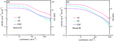 | ||
| Fig. 12 Relationship between EL efficiencies and luminance for the optimized devices. (a) Device A2 and (b) device B2. | ||
The optimal EL performances are realized in device A2 employing PhSeDB as the emitter. Remarkably, device A2 exhibits exceptional EL characteristics, boasting a maximum external quantum efficiency (EQE) of 18.2%, current efficiency (CE) of 53.6 cd A−1, and power efficiency (PE) of 49.6 lm W−1, all achieved at a maximum luminance (Lmax) of 3000.9 cd m−2 at 18.5 V and a low turn-on voltage (Vturn-on) of 3.0 V (Fig. 11d and Table 1). Notably, these represent the best reported performances among purely organic phosphorescent emitters in the existing literature (Fig. 13 and Table S2†). Device B2, based on PhSeB, also demonstrates commendable EL capabilities, featuring an EQE of 10.5%, CE of 29.5 cd A−1, and PE of 24.1 lm W−1, respectively (Fig. 9d and Table S4†). Additionally, this device exhibits simultaneous TADF and RTP EL emission. The lower EL performances of device B2, when compared to device A2, can be ascribed to the comparatively weaker charge transport characteristics. This is supported by the higher current density observed in device B2 at high voltage, indicating weaker charge transport performance of PhSeB (Fig. 11d). These favorable outcomes substantiate that the incorporation of n → π* transitions and heavy atom Se into SOCT-ISC systems constitutes an effective molecular design concept for achieving pure phosphorescence emission at room temperature.
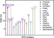 | ||
| Fig. 13 Maximum EQEs of currently reported POPLEDs based on RTP emitters versus this work, detailed device data seen in Table S2.† | ||
Conclusions
In summary, two efficient bipolar metal-free orange RTP emitters, PhSeB and PhSeDB, have been developed based on a promising molecular design concept. This concept involves incorporating enhanced n → π* transitions, magnified electron-coupling and the heavy atom effect into the SOCT-ISC systems. PhSeDB, with an A–D–A configuration, exhibits enhanced n → π* transitions and electron coupling compared to PhSeB with a D–A configuration. As a result, PhSeDB shows higher SOCMEs for S1 ↔ Tn (n = 1, 2, 3) and T1 ↔ S0 than PhSeB. This enhancement facilitates the efficient utilization of triplet excitons, enabling PhSeDB to achieve pure RTP emission with the highest phosphorescence quantum yield (ca. 0.78). Utilizing PhSeDB as a phosphorescent emitter, POPLEDs achieve the state-of-the-art EQE of 18.2% and luminance of 3000 cd m−2 with pure electro-phosphorescence spectra. Overall, considering the influential role of n → π* transitions, electron coupling and the heavy atom effect of the Se atom in the SOCT-ISC mechanism, this strategic molecular configuration alteration emerges as a particularly advantageous approach in realizing high-performance POPLEDs.Data availability
The experimental and theoretical data relevant to this work are provided in the manuscript, so there is no need to store them in data repositories.Author contributions
Daokun Zhong and Guijiang Zhou conceived and supervised the idea. Daokun Zhong performed all experiments. Siqi Liu contributed to device preparation. Ling Yue provided support for the theoretical calculations. All authors discussed the results and wrote the manuscript.Conflicts of interest
There are no conflicts to declare.Acknowledgements
This work was supported by the National Natural Science Foundation of China (52161145411, 22375158, 22175137 and 51803163), the Natural Science Foundation of Shaanxi Province (2023-JC-QN-0144), the Fundamental Research Funds for the Central Universities (xzy012022020 and xzy012023039), the China Postdoctoral Science Foundation (2022M722525), and the Shaanxi Province Postdoctoral Science Foundation (2023BSHEDZZ25 and 2023BSHEDZZ28). The characterization assistance from the Instrument Analysis Center of Xi'an Jiaotong University is also acknowledged.Notes and references
-
(a) Y. C. Zhu, L. Zhou, H. Y. Li, Q. L. Xu, M. Y. Teng, Y. X. Zheng, J. L. Zuo, H. J. Zhang and X. Z. You, Adv. Mater., 2011, 23, 4041–4046 CrossRef CAS PubMed
; (b) C.-H. Yang, M. Mauro, F. Polo, S. Watanabe, I. Muenster, R. Fröhlich and L. De Cola, Chem. Mater., 2012, 24, 3684–3695 CrossRef CAS
; (c) C. L. Kim, J. Jeong, H. J. Jang, K. H. Lee, S.-T. Kim, M.-H. Baik and J. Y. Lee, J. Mater. Chem. C, 2021, 9, 8233–8238 RSC
; (d) X. Song, G. Lu, Y. Man, J. Zhang, S. Chen, C. Han and H. Xu, Angew. Chem., Int. Ed., 2023, 62, e202311937 CrossRef PubMed
; (e) Y. Sun, L. Jiang, L. Liu, Y. Chen, W. W. Xu, J. Niu, Y. Qin, X. Xu and Y. Liu, Adv. Opt. Mater., 2023, 11, 2300326 CrossRef CAS
.
-
(a) L. Bian, H. Shi, X. Wang, K. Ling, H. Ma, M. Li, Z. Cheng, C. Ma, S. Cai, Q. Wu, N. Gan, X. Xu, Z. An and W. Huang, J. Am. Chem. Soc., 2018, 140, 10734–10739 CrossRef CAS PubMed
; (b) B. Song, W. Shao, J. Jung, S.-J. Yoon and J. Kim, ACS Appl. Mater. Interfaces, 2020, 12, 6137–6143 CrossRef CAS PubMed
; (c) J. Yu, Z. Sun, H. Ma, C. Wang, W. Huang, Z. He, W. Wu, H. Hu, W. Zhao and W. H. Zhu, Angew. Chem., Int. Ed., 2023, 62, e202316647 CrossRef CAS PubMed
; (d) Z. Wang, M. Gao, M. Wei, S. Ren, X.-T. Hao and W. Qin, ACS Nano, 2019, 13, 4705–4711 CrossRef CAS PubMed
.
-
(a) Z. Xu, Y. He, H. Shi and Z. An, Smart Mater., 2022, 4, e1139 Search PubMed
; (b) H. Wang, C. Peng, M. Chen, Y. Xiao, T. Zhang, X. Liu, Q. Chen, T. Yu and W. Huang, Angew. Chem., Int. Ed., 2023, 63, e202316190 CrossRef PubMed
.
-
(a) Z. Yang, Z. Mao, X. Zhang, D. Ou, Y. Mu, Y. Zhang, C. Zhao, S. Liu, Z. Chi, J. Xu, Y. C. Wu, P. Y. Lu, A. Lien and M. R. Bryce, Angew. Chem., Int. Ed., 2016, 55, 2181–2185 CrossRef CAS PubMed
; (b) W. Wang, Y. Zhang and W. J. Jin, Coord. Chem. Rev., 2020, 404, 213107 CrossRef CAS
; (c) G. Yang, A. Lv, Z. Xu, Z. Song, K. Shen, C. Lin, G. Niu, H. Ma, H. Shi and Z. An, J. Mater. Chem. C, 2022, 10, 13747–13752 RSC
.
- Z. F. Liu, X. Chen, W. X. Wu, G. Q. Zhang, X. Li, Z. Z. Li and W. J. Jin, Spectrochim. Acta, Part A, 2020, 224, 117428 CrossRef CAS PubMed
.
- H. Shi, L. Song, H. Ma, C. Sun, K. Huang, A. Lv, W. Ye, H. Wang, S. Cai, W. Yao, Y. Zhang, R. Zheng, Z. An and W. Huang, J. Phys. Chem. Lett., 2019, 10, 595–600 CrossRef CAS PubMed
.
- Y. Liu, G. Zhan, Z.-W. Liu, Z.-Q. Bian and C.-H. Huang, Chinese Chem. Lett., 2016, 27, 1231–1240 CrossRef CAS
.
-
(a) M. Li, W. Xie, X. Cai, X. Peng, K. Liu, Q. Gu, J. Zhou, W. Qiu, Z. Chen, Y. Gan and S. J. Su, Angew. Chem., Int. Ed., 2022, 61, e202209343 CrossRef CAS PubMed
; (b) H. Liu, Y. Gao, J. Cao, T. Li, Y. Wen, Y. Ge, L. Zhang, G. Pan, T. Zhou and B. Yang, Mater. Chem. Front., 2018, 2, 1853–1858 RSC
; (c) Z. Yu, Y. Wu, L. Xiao, J. Chen, Q. Liao, J. Yao and H. Fu, J. Am. Chem. Soc., 2017, 139, 6376–6381 CrossRef CAS PubMed
.
-
(a) Z. Cheng, X. Wang, J. Zhao, S. Wang, X. Wu, H. Tong and L. Wang, Macromolecules, 2023, 56, 2972–2979 CrossRef CAS
; (b) D. R. Lee, K. H. Lee, W. Shao, C. L. Kim, J. Kim and J. Y. Lee, Chem. Mater., 2020, 32, 2583–2592 CrossRef CAS
.
- C. L. Kim, J.-M. Kim, H. Jang, D. R. Lee and J. Y. Lee, ACS Appl. Energy Mater., 2022, 5, 4985–4990 CrossRef CAS
.
- C. L. Kim, J. Jeong, D. R. Lee, H. J. Jang, S.-T. Kim, M.-H. Baik and J. Y. Lee, J. Phys. Chem. Lett., 2020, 11, 5591–5600 CrossRef CAS PubMed
.
-
(a) D. Liu, A. M. El-Zohry, M. Taddei, C. Matt, L. Bussotti, Z. Wang, J. Zhao, O. F. Mohammed, M. Di Donato and S. Weber, Angew. Chem., Int. Ed., 2020, 59, 11591–11599 CrossRef CAS PubMed
; (b) M. Lv, Y. Yu, M. E. Sandoval-Salinas, J. Xu, Z. Lei, D. Casanova, Y. Yang and J. Chen, Angew. Chem., Int. Ed., 2020, 59, 22179–22184 CrossRef CAS PubMed
; (c) J. T. Buck, A. M. Boudreau, A. DeCarmine, R. W. Wilson, J. Hampsey and T. Mani, Chem, 2019, 5, 138–155 CrossRef CAS
; (d) Z. Wang and J. Zhao, Org. Lett., 2017, 19, 4492–4495 CrossRef CAS PubMed
; (e) Z. Wang, M. Ivanov, Y. Gao, L. Bussotti, P. Foggi, H. Zhang, N. Russo, B. Dick, J. Zhao, M. Di Donato, G. Mazzone, L. Luo and M. Fedin, Chem.–Eur. J., 2020, 26, 1091–1102 CrossRef CAS PubMed
.
-
(a) Y. Hou, I. Kurganskii, A. Elmali, H. Zhang, Y. Gao, L. Lv, J. Zhao, A. Karatay, L. Luo and M. Fedin, J. Chem. Phys., 2020, 152, 114701 CrossRef CAS PubMed
; (b) M. L. Williams, I. Schlesinger, R. M. Jacobberger and M. R. Wasielewski, J. Am. Chem. Soc., 2022, 144, 18607–18618 CrossRef CAS PubMed
.
-
(a) Y. Liang, C. Xu, H. Zhang, S. Wu, J. A. Li, Y. Yang, Z. Mao, S. Luo, C. Liu, G. Shi, F. Sun, Z. Chi and B. Xu, Angew. Chem., Int. Ed., 2023, 62, e202217616 CrossRef CAS PubMed
; (b) Y. Cai, X. Ji, Y. Zhang, C. Liu, Z. Zhang, Y. Lv, X. Dong, H. He, J. Qi, Y. Lu, D. Ouyang, W. Zhao and W. Wu, Aggregate, 2022, 4, e277 CrossRef
.
-
(a) M. A. Filatov, S. Karuthedath, P. M. Polestshuk, H. Savoie, K. J. Flanagan, C. Sy, E. Sitte, M. Telitchko, F. Laquai, R. W. Boyle and M. O. Senge, J. Am. Chem. Soc., 2017, 139, 6282–6285 CrossRef CAS PubMed
; (b) M. A. Filatov, S. Karuthedath, P. M. Polestshuk, S. Callaghan, K. J. Flanagan, M. Telitchko, T. Wiesner, F. Laquai and M. O. Senge, Phys. Chem. Chem. Phys., 2018, 20, 8016–8031 RSC
; (c) D. J. Gibbons, A. Farawar, P. Mazzella, S. Leroy-Lhez and R. M. Williams, Photochem. Photobiol. Sci., 2020, 19, 136–158 CrossRef CAS PubMed
.
-
(a) M. Imran, A. M. El-Zohry, C. Matt, M. Taddei, S. Doria, L. Bussotti, P. Foggi, J. Zhao, M. Di Donato, O. F. Mohammed and S. Weber, J. Mater. Chem. C, 2020, 8, 8305–8319 RSC
; (b) J. Zhao, K. Xu, W. Yang, Z. Wang and F. Zhong, Chem. Soc. Rev., 2015, 44, 8904–8939 RSC
.
-
(a) Q. Zhang, D. Tsang, H. Kuwabara, Y. Hatae, B. Li, T. Takahashi, S. Y. Lee, T. Yasuda and C. Adachi, Adv. Mater., 2015, 27, 2096–2100 CrossRef CAS PubMed
; (b) D. Zhong, Y. Yu, D. Song, X. Yang, Y. Zhang, X. Chen, G. Zhou and Z. Wu, ACS Appl. Mater. Interfaces, 2019, 11, 27112–27124 CrossRef CAS PubMed
; (c) D. Zhong, Y. Yu, L. Yue, X. Yang, L. Ma, G. Zhou and Z. Wu, Chem. Eng. J., 2021, 413, 127445 CrossRef CAS
.
-
(a) P. K. Samanta, D. Kim, V. Coropceanu and J.-L. Brédas, J. Am. Chem. Soc., 2017, 139, 4042–4051 CrossRef CAS PubMed
; (b) X. Chen, X. Xiao and J. Zhao, J. Mater. Chem. C, 2022, 10, 4546–4557 RSC
.
-
(a) Y. Zhang and S. R. Forrest, Phys. Rev. Lett., 2012, 108, 267404 CrossRef PubMed
; (b) T. Furukawa, H. Nakanotani, M. Inoue and C. Adachi, Sci. Rep., 2015, 5, 8429 CrossRef CAS PubMed
.
Footnote |
| † Electronic supplementary information (ESI) available. CCDC 2295656. For ESI and crystallographic data in CIF or other electronic format see DOI: https://doi.org/10.1039/d4sc01200c |
| This journal is © The Royal Society of Chemistry 2024 |

