
 Open Access Article
 This Open Access Article is licensed under a
 Creative Commons Attribution 3.0 Unported Licence
In situ formation and photo patterning of emissive quantum dots in small organic molecules
Ashu K.
Bansal
a,
Muhammad T.
Sajjad
a,
Francesco
Antolini
b,
Lenuta
Stroea
b,
Paulius
Gečys
c,
Gediminas
Raciukaitis
cd,
Pascal
André
a,
Andreas
Hirzer
e,
Volker
Schmidt
e,
Luca
Ortolani
f,
Stefano
Toffanin
g,
Sybille
Allard
h,
Ullrich
Scherf
h and
Ifor D. W.
Samuel
*a
aOrganic Semiconductor Centre, SUPA, School of Physics and Astronomy, University of St Andrews, North Haugh, St Andrews, Fife KY16 9SS, UK. E-mail: idws@st-andrews.ac.uk
bENEA UTTMATF, Via Ravegnana 186, 48018 Faenza, RA, Italy
cCenter for Physical Sciences and Technology, Savanoriu Ave. 231, LT-02300 Vilnius, Lithuania
dEKSPLA UAB, Savanoriu Ave. 237, LT-02300 Vilnius, Lithuania
eJoanneum Research, Forschungsgesellschaft mbH, MATERIALS – Institute for Surface Technologies and Photonics, Franz-Pichler-Straße 30, 8160 Weiz, Austria
fCNR IMM – Bologna Section, Via Gobetti 101, Bologna (BO), Italy
gConsiglio Nazionale delle Ricerche (CNR) – Istituto per lo Studio dei Materiali Nanostrutturati (ISMN), Via P. Gobetti, 101, Bologna, Italy
hInstitut für Polymertechnologie Bergische Universität Wuppertal, Gauss-Strasse 20, 42097 Wuppertal, Germany
First published on 18th May 2015
Abstract
Nanostructured composites of inorganic and organic materials are attracting extensive interest for electronic and optoelectronic device applications. Here we report a novel method for the fabrication and patterning of metal selenide nanoparticles in organic semiconductor films that is compatible with solution processable large area device manufacturing. Our approach is based upon the controlled in situ decomposition of a cadmium selenide precursor complex in a film of the electron transporting material 1,3,5-tris(N-phenyl-benzimidazol-2-yl)-benzene (TPBI) by thermal and optical methods. In particular, we show that the photoluminescence quantum yield (PLQY) of the thermally converted CdSe quantum dots (QDs) in the TPBI film is up to 15%. We also show that laser illumination can form the QDs from the precursor. This is an important result as it enables direct laser patterning (DLP) of the QDs. DLP was performed on these nanocomposites using a picosecond laser. Confocal microscopy shows the formation of emissive QDs after laser irradiation. The optical and structural properties of the QDs were also analysed by means of UV-Vis, PL spectroscopy and transmission electron microscopy (TEM). The results show that the QDs are well distributed across the film and their emission can be tuned over a wide range by varying the temperature or irradiated laser power on the blend films. Our findings provide a route to the low cost patterning of hybrid electroluminescent devices.
Introduction
Patterning of optoelectronic devices is a challenge – particularly for the development of scalable optoelectronic devices including solar cells,1,2 light-emitting devices (LEDs)3 and field effect transistors.4 A wide variety of techniques including nanoimprint,5 photolithography6 and scanning-probe lithography7 for making features on the nanometer to micrometer length scale are continuously being developed and reported for patterning. However, most of these techniques rely on surface modification of samples and require time consuming processes which are not compatible with large scale production of organic optoelectronic devices.8 Furthermore, using such techniques once a photomask is fabricated, its design is fixed. For these reasons, the development of alternative direct, maskless, high-resolution patterning techniques to fabricate patterns at low temperature without using high vacuum deposition has attracted special attention in recent years.9,10 Direct laser patterning (DLP) of nanoparticles provides a most suitable alternative in this direction for the fabrication of hybrid organic/nanoparticle based devices. DLP techniques do not require complex laser systems11 or the use of dangerous chemical post treatments12 so they can be advantageous in optoelectronic devices. Furthermore, they can provide spatially selective tailoring of the specific properties of the resulting nanocomposites, which are highly desired for optoelectronic devices for different applications.Here we demonstrate a laser patterning to give in situ formation of QDs. Our results provide a pathway for simple patterning of the light-emitting area in hybrid devices. Our approach is based upon the controlled in situ decomposition of a cadmium selenide precursor complex in a film of 1,3,5-tris(N-phenyl-benzimidazol-2-yl)-benzene (TPBI), a widely used electron transport material which plays a key role in organic light emitting devices.13 We show the formation of light emitting dots of CdSe with a photoluminescence quantum yield (PLQY) up to 15% in the resulting film. We show that the properties of the in situ formed quantum dots depend on the concentration of the solution, blend ratio of the precursor, baking temperature and laser irradiance. Confocal microscopy shows the formation of the emissive QDs after laser processing. The optical and structural properties of the QDs are also analysed by means of UV-Vis, photoluminescence (PL) spectroscopy, transmission electron microscopy (TEM) and atomic force microscopy (AFM).
In most reported strategies, hybrid optoelectronic devices are prepared by mixing organic materials with inorganic ones in a common solvent, often this approach is associated with chemical grafting and ligand exchange techniques applied prior to mixing so as to control the solution properties, miscibility, the surface states and the electronic structure of the nanoparticles.14–17 For example, in the widely reported approach of blending materials, the performance of such devices depends critically on the ability to control materials and interface structure at the nanometer length scale.18 In an alternative approach, in situ formed QDs are directly generated inside a polymer matrix by the decomposition of appropriate molecular precursors using either thermal, optical or chemical methods.19–21 In this direction we have recently reported the formation of light-emitting dots by thermolysis of precursors inside the conjugated polymer matrix.21 The advantage of this approach is that there is no need to perform any ligand exchange after the synthesis of the QDs as it is the polymer itself which controls the growth of nanoparticles and thereby removes the need for additional capping agents. Another advantage of this process is that it does not require extracting the QDs from their synthetic media to prepare a device, which reduces the number of steps as well as the use of solvents which are often expensive and toxic. This approach has the potential to allow the development of greener fabrication methods which moderate the overall environmental impact of device manufacturing by implementing cleaner chemistry pathways. The use of temperature to drive QD formation is the most common strategy implemented in solution, however, when this methodology is transferred to thin films for QD in situ synthesis it benefits from a very interesting twist, because the thermal treatment can be selectively induced in different regions by using an appropriate thermal source, such as a laser. There are a few reports in which a polymer TOPAS or polymethylmethacrylate (PMMA) has been used with CdS based precursors in nanocomposite films and the effect of UV radiation using lasers of different wavelengths have been studied to have a well defined patterned area on the nanocrystals.20,22 However there are no reports where light emitting quantum dots are selectively produced and patterned in the organic semiconductor molecules used in fabrication of organic light emitting devices.
The paper is organized as follows. We first discuss the optical properties of the nanocomposite films of TPBI and the precursor after thermolysis. Then the structural properties of such in situ formed QDs are defined using TEM and AFM. Finally, the photo-patterning of the emissive QDs using a picosecond laser is demonstrated and discussed.
Experimental section
Materials and film preparation
The electron transporting material 1,3,5-tris(N-phenyl-benzimidazol-2-yl)-benzene (TPBI) was bought from Lumtec and was used without any further purification. The protocol for the synthesis of the CdSe precursor cadmium 2-(N,N-dimethylamino)ethylselenolate (CdDMASe) was adapted from the work23 of Kedarnath et al. First it involved making an aliphatic diselenide compound and then reacting it with a Cd[II] salt to give the metalorganic precursor. This single source precursor bearing two Me2NCH2CH2Se fragments, shows good solubility and has clean thermal decomposition generating cadmium selenide (CdSe) QDs. The precursor is soluble in toluene, stable under room temperature conditions and can be stored for weeks.Neat films of the precursor alone and nanocomposite films of the TPBI/precursor blend were prepared by spin-coating in toluene solution at 1500 rpm onto fused silica substrates. The films used for spin-coating consisted of either precursor powder alone or precursor/TPBI in a ratio of 4![[thin space (1/6-em)]](https://www.rsc.org/images/entities/char_2009.gif) :1 in toluene solvent at 50 mg ml−1 concentration. These films were baked at different temperatures inside a low vacuum 8 × 10⁻² mbar for thermolysis.
:1 in toluene solvent at 50 mg ml−1 concentration. These films were baked at different temperatures inside a low vacuum 8 × 10⁻² mbar for thermolysis.
Photophysical and structural measurements
Absorption measurements were carried out using a Cary Varian 300 spectrometer. Photoluminescence spectra were recorded using a JY Horiba Fluoromax 2 fluorimeter, with an excitation wavelength of 305 nm. Solid-state PLQY measurements of thin films were performed in an integrating sphere under a nitrogen purge24 in a Hamamatsu C9920-02 luminescence measurement system.We have also used an Olympus BX51 optical microscope and an epi-fluorescence microscope with Hg-lamp excitation to collect the fluorescence from the samples. To distinguish the excitation and fluorescence spectra a set of filters U-MWU2 was used in the microscope. The excitation wavelength was in the range 330–385 nm and the fluorescence signal was averaged over the spectrum for wavelengths >420 nm.
The transmission electron microscopy (TEM) measurements were performed with a Philips Tecnai F20 Schottky Field emission gun (FEG) instrument operating at 200 kV. The images were processed with Digital micrograph and ImageJ software. The QD size was determined manually, on the basis of the high-resolution transmission electron microscopy (HRTEM) images obtained. The chemical composition was verified by means of energy dispersive spectrometry (EDS) with an EDAX Phoenix spectrometer equipped with an ultra-thin window detector and TEM image and along with analysis software. The samples for TEM characterization were deposited over a TEM grid with spin-coating at 1500 rpm on copper TEM grids covered by Quantifoil® Holey Carbon films.
Atomic force microscopy (AFM) topographical images were collected with an NT-MDT Solver Scanning Probe Microscope in the tapping mode with a silicon tip. An average value of root-mean-square (RMS) roughness was calculated for a scan area of 10 μm × 10 μm. The cluster distribution (number of clusters for μm2) has been calculated as average of the number of the clusters in four different areas of the backed samples. The surface coverage (%) has been determined by multiplying the cluster area for the cluster distribution.
Photo-patterning
Laser-patterning experiments were performed using a laser micro-processing system with the fourth harmonic of a picosecond laser (Ekspla Atlantic, 266 nm wavelength, 10 ps pulse duration, 100 kHz pulse repetition rate). An external electro-optical pulse picker was used for laser beam switching and average power control. During the film modification average laser powers from 0.1 to 3 mW were used. The sample was placed on an X–Y–Z sample stage where the X–Y stage controls the sample movement and the Z stage was used for the laser beam focus adjustment. An objective with a focal length of 100 mm was used for laser beam focusing on the sample. The laser irradiated spot size on the films was ∼20 μm. Areas of nanocomposite films with a size from 1 × 1 up to 5 × 5 mm2 were irradiated by scanning the laser beam. All experiments were conducted in a closed chamber with a fused silica window and it was filled with 99.9% nitrogen.Results and discussion
Optical properties of nanocomposite films of TPBI and CdDMASe precursors
Fig. 1a shows the chemical structure of a CdSe based precursor cadmium 2-(N,N-dimethylamino)ethylselenolate (CdDMASe) which belongs to the family of cadmium chalcogenolato complexes.25 These kinds of complexes are usually insoluble, because of their polymeric structure.26,27 However in the case of CdDMASe the organic ligand with its nitrogen atoms can coordinate to the Cd, as shown in Fig. 1a, and block the formation of the inorganic polymer which enhances the molecule solubility.28 The precursor solubility is of great importance to ensure a homogeneous distribution of QDs inside the host matrix and represents a prerequisite to obtain reproducible films by solution-processing and device manufacturing.29 The chemical structure of the electron transport material 1,3,5-tris(N-phenyl-benzimidazol-2-yl)-benzene (TPBI) used as a host material with this precursor is shown in Fig. 1b. The absorption and fluorescence spectra of the neat TPBI film together with absorption spectra of the CdSe precursor in the solid state is shown in Fig. 2a. As shown in Fig. 2a, TPBI absorbs in the UV region with a peak at 305 nm and emits with a fluorescence peak at 380 nm when the sample is excited at 305 nm. The CdDMASe precursor film also absorbs in UV with peak absorbance below 280 nm but does not show any emission even when excited at different excitation wavelengths from 280 to 380 nm.21 We have also measured the photoluminescence quantum yield of the TPBI neat film using an integrating sphere purged with nitrogen and found it to be 45% when the film was excited at 305 nm. | ||
| Fig. 1 (a) Chemical structure of precursor CdDMASe and (b) TPBI; (c) mechanism of cadmium selenolate thermolytic decomposition. | ||
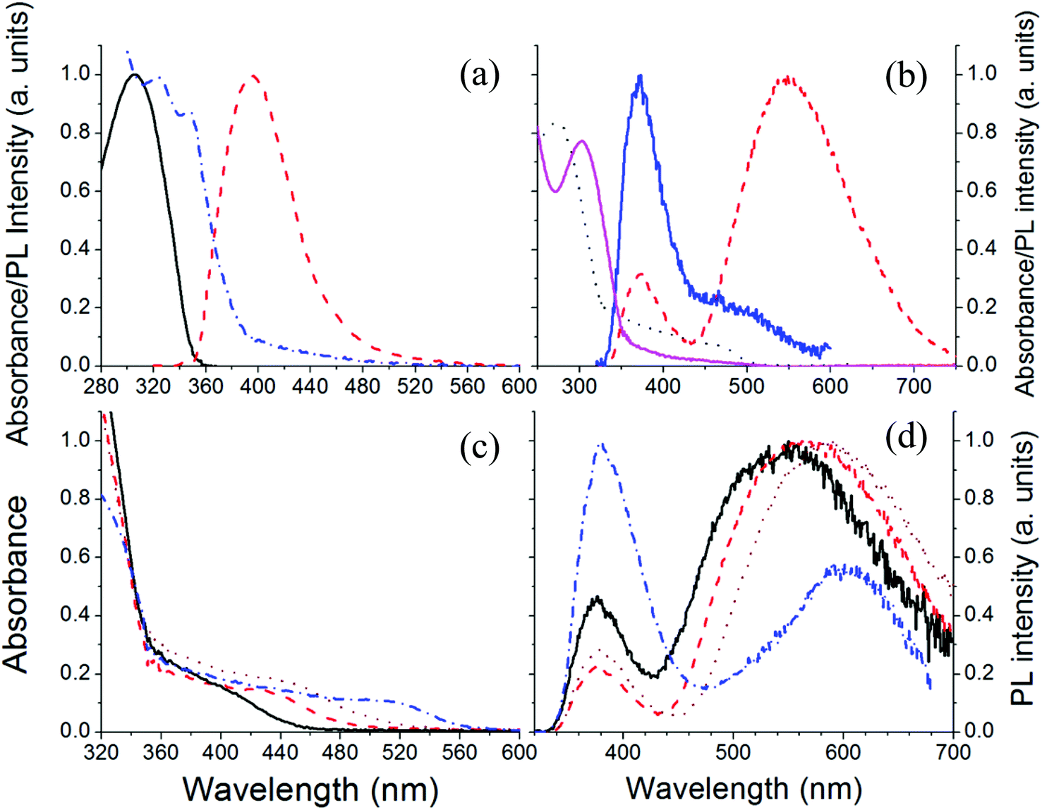 | ||
| Fig. 2 (a) Absorption (black solid line) and photoluminescence (PL) spectra (red dotted) of TPBI as a thin film. The blue dash dotted line shows the absorption spectrum of the precursor CdDMASe as a thin film; (b) absorption and PL spectra of the TPBI/CdDMASe precursor film before baking (magenta and blue solid lines respectively) and after baking at 160 °C for 15 minutes (absorption, black dotted line; emission, red dashed line); (c) and (d) absorption and PL spectra of TPBI/CdDMASe precursor films after baking at one of 4 different temperatures: 140 °C (solid line) 150 °C (dashed line), 160 °C (dotted line) and 180 °C (dash dotted line) for 15 minutes. Fluorescence was excited at 305 nm. | ||
In our process of photopatterning, the laser produces localized heating which decomposes the precursor leading to the formation of QDs. We have studied the effect of temperature on the formation of QDs within the nanocomposite films. The decomposition mechanism for this precursor having a cadmium selenolate complex is shown in Fig. 1c. The schematic reaction shows that the thermolysis of this precursor leads to the formation of CdSe with the evolution of Se(CH2CH2NMe2)2.30,31 This mechanism is in good agreement with the thermogravimetric data of the complex having a mass loss compatible with the proposed reaction.23Fig. 2b shows the absorption and fluorescence signals of the TPBI/precursor nanocomposite film blended in the molar ratio of 1:4, before and after the thermal process. Before baking, the absorption in the nanocomposite is dominated by TPBI with a strong absorption peak at 305 nm and there is a tail at longer wavelengths due to the absorption of the precursor in the nanocomposite. The nanocomposite film before baking emits poorly with most of the emission coming from the TPBI and only a small shoulder at longer wavelengths possibly due to energy transfer from TPBI to the precursor, as the precursor itself is non-emissive.32 After baking the sample at 160 °C for 15 minutes the absorption spectrum peak is blue-shifted by 10 nm and the tail at longer wavelengths absorbs strongly due to the QD formation after precursor decomposition. The fluorescence spectra of the nanocomposite films after baking show interesting features with emission due to two different species. The first small peak at 380 nm is due to TPBI and the second peak at 590 nm with broad emission is possibly due to QDs. This emission is independent of the excitation wavelength (data not shown).
To get a clear indication of the formation of QDs after precursor thermolysis we have conducted a decomposition study under different time/temperature conditions. Fig. 2c shows the absorption spectra of the nanocomposite films baked at four different temperatures. It is clear from the figure that after baking a well-defined shoulder appears in the absorption in the region of 420 nm. For higher temperatures this feature shifts towards 520 nm. This red shift behavior confirms that the signal is due to decomposition of the precursor and formation of QDs. The absence of well-resolved peak like structures can be attributed to the polydispersity or the surface states of the QDs.32Fig. 2d shows the fluorescence spectra of the nanocomposite films following excitation at 305 nm at the peak of the absorption of TPBI. For instance, the nanocomposite film baked at 140 °C for 15 minutes shows emission of the TPBI and an extra emission at longer wavelengths. After baking at higher temperatures the emission corresponding to TPBI decreases and contribution due to QDs increases. This result can be due to two different effects, i.e. QD formation and improved energy transfer between QDs and TPBI. Indeed the decomposition temperature of the selenolate complex23 is about 160 °C and so, as soon as the temperature increases from 140 °C to 160 °C the QDs acquire more regular structure which improves the energy transfer between the TPBI and QDs. Higher temperature can also improve the removal of the reaction by-products, i.e. SeR2 from the thin film (Fig. 1c) facilitating the energy transfer between TPBI and the QDs.33 At even higher temperatures the emission due to the QDs starts decreasing possibly due to aggregate formation of the QDs. Furthermore as we tested the thermal stability of neat TPBI under the same time/temperature conditions and found no such evidence of emission at longer wavelengths, so we assign the extra emission at longer wavelengths to QD formation only.
PLQY measurements give further insight into the properties of these nanocomposite films and were performed with excitation at 305 nm. Before baking, PLQY of TPBI is strongly quenched by the precursor in the nanocomposite films and reduced to 0.5% from 45% in neat films. After thermolysis of the blend, the PLQY of the QDs is extracted from the total PLQY of the nanocomposite films by calculating the emission contribution from 500 to 900 nm. The maximum PLQY obtained for the QDs is 15.5% after heating at 160 °C for 15 minutes. The PLQY decreases to 1% by heating at 200 °C. The decrease of the PLQY can be attributed to trapping of electrons in surface-defect states with further increase of the density of trap states at higher temperatures resulting from depletion of the hybrid films of the QD precursors.18,34 To understand further, fluorescence microscopy was performed on nanocomposite films before and after baking under various excitation wavelengths in an argon gas environment.
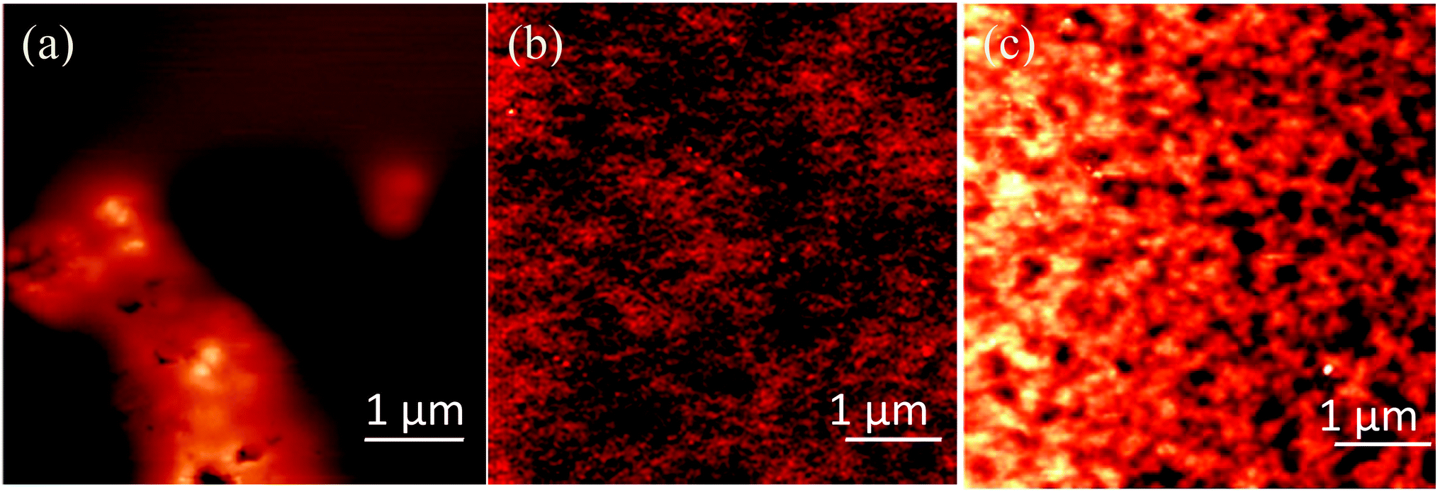
Fig. 3a and b show the fluorescence microscopy images when samples are excited with UV light and Fig. 3c and d show when samples are excited by the green line of a mercury lamp (546 nm). The scale bar for the images is 50 μm. Before baking the samples there is weak blue emission from the blend under UV light excitation (Fig. 3a) which we attribute it to TPBI, as the QD precursor is non-emissive. Under green light excitation no fluorescence was observed at all (Fig. 3c). After baking the samples at 160 °C for 15 minutes, we see clear emission under UV and green excitations as shown in Fig. 3b and d respectively. When we have baked the samples at higher temperatures, the fluorescence decreases rapidly and we see large clusters of nanoparticles (data not shown). These results are in correlation with PLQY results where the emission efficiency of QDs decreases at higher temperatures. The broad emission of the QDs obtained is due to the formation of surface defects. Trap emission has often been related to low crystallinity, selenide excess or other defects at the interface of the nanocrystals.32 However, band edge and trap emissions are often observed together in CdSe nanocrystals.35 Increasing the amount of surface defects of the nanoparticles can enhance enormously the trap state emission with respect to the band-edge recombination mechanism or even suppress it entirely. The other possible explanation for the reduction in PLQY could be aggregation of the QDs at the higher baking temperature. We have therefore investigated the structure of the films by AFM and TEM.
 | ||
| Fig. 3 Fluorescence microscopic images of (a) untreated film and (b) baked film at 160 °C for 15 minutes with excitation under UV line of a mercury lamp; (c) untreated film and (d) baked film at 160 °C for 15 minutes with excitation under green light (546 nm). | ||
Structural characterization of nanocomposite films of TPBI and CdDMASe precursors
To obtain further evidence of nanoparticle synthesis, transmission electron microscopy (TEM) measurements were performed. The analyses were carried out on films deposited and baked directly on a TEM grid to observe the particle distribution in the films. Fig. 4a shows a low magnification view of the films casted over a standard TEM grid with a holey carbon film for support. High resolution image of these films is shown in Fig. 4b, which also does not provide any evidence of QD formation before the thermal treatment. Furthermore Fig. 4c shows the Fast Fourier Transform (FFT) spectrum of the area in Fig. 4b, revealing no crystalline reflection, with the typical diffuse structure of amorphous materials. During measurements of such films special attention was paid by using low density current and short observation time so that the electron beam itself does not cause the thermolysis process.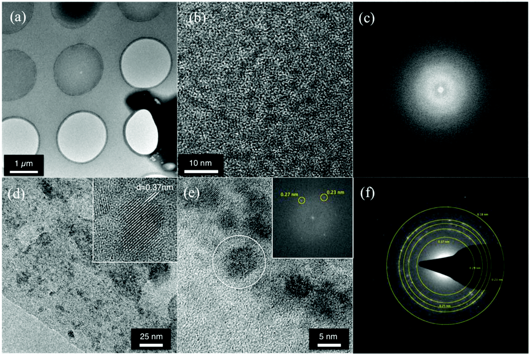 | ||
| Fig. 4 TEM characterization of the TPBI samples. (a) Low magnification image of the film casted over the holey carbon film of the TEM grid. (b) High resolution image of the clusters composing the film before baking. (c) FFT of (b) showing no lattice reflection from the clusters. (d) Low resolution image of the film baked at 140 °C for 15 minutes with the inset showing high resolution image of an individual nanoparticle, indicating lattice fringes of CdSe crystals. (e) High-resolution image of a group of nanocrystals. (Inset) FFT of the particle highlighted, showing reflections corresponding to CdO crystal lattice. (f) SAED pattern showing ring like reflections from CdSe, SeO, and CdO nanocrystals. | ||
TEM results for the films after baking at 140 °C for 15 minutes under low vacuum conditions are shown in Fig. 4d–f. Low magnification TEM micrograph in Fig. 4d shows that the polydispersity of the particles in terms of size and morphology is large and highly inhomogeneous. There are big particles with irregular morphology and also small particles together with some rod-like structures. The inset of Fig. 4d shows an individual nanocrystal, showing lattice fringes spaced by 0.37 nm, corresponding to a (100) family of planes in the CdSe crystal lattice. The high resolution image in Fig. 4e shows a group of large irregular clusters. The inset shows the FFT spectrum of the large particle highlighted in Fig. 4e, revealing reflections corresponding to 0.27 nm and 0.23 nm lattice spacing, compatible with CdO crystals. The diffraction pattern of a wide area of the sample is obtained by the SAED technique and the results are shown in Fig. 4f. The diffraction pattern shows typical powder like ring reflections, corresponding to interplanar distances of 0.37 nm, 0.29 nm, 0.25 nm, 0.23 nm and 0.18 nm, compatible with the presence of a mixture of CdSe, CdO and SeO nanocrystals in the films. This suggests that precursor segregation has occurred within the sample and that baking at 140 °C for 15 minutes only leads to a partial formation of CdSe nanoparticles. This specific time/temperature condition is then enough to decompose the precursors and partial nucleation of the QDs but not enough to complete sufficient nucleation and growth of the nanoparticles.
Fig. 5 shows additional TEM results for the nanocomposite films baked at 160 °C for 15 minutes. The high-resolution image in Fig. 5a shows that the particles are highly crystalline. This is confirmed by FFT (inset of Fig. 5a) of the HRTEM micrograph, showing the typical lattice spacing of the CdSe hexagonal phase, with highlighted reflections corresponding to (002), (110) and (112) families of planes, spaced to 0.35 nm, 0.21 nm and 0.18 nm respectively. The size distribution analysis was performed by direct observation from the HRTEM images. The results of the analysis are summarized in the histogram of Fig. 5b. As reported in the figure, a Gaussian fit of the data resulted in an average diameter of 3.5 nm, with a standard deviation of 0.9 nm. The size distribution is of about 26% large compared with solution synthesis pathways but nonetheless in the range of literature values35 reported for CdSe QDs and is below the threshold for the Bohr exciton radius.34 In Fig. 5c the EDX spectrum shows the Cd and Se peaks, with no particular contaminant species, as the copper signal comes from the TEM grid used as the support. As discussed above aggregate formation and faster depletion of the QD precursors at higher baking temperatures explain the reduction in PLQY of the emissive QDs under these preparation conditions.
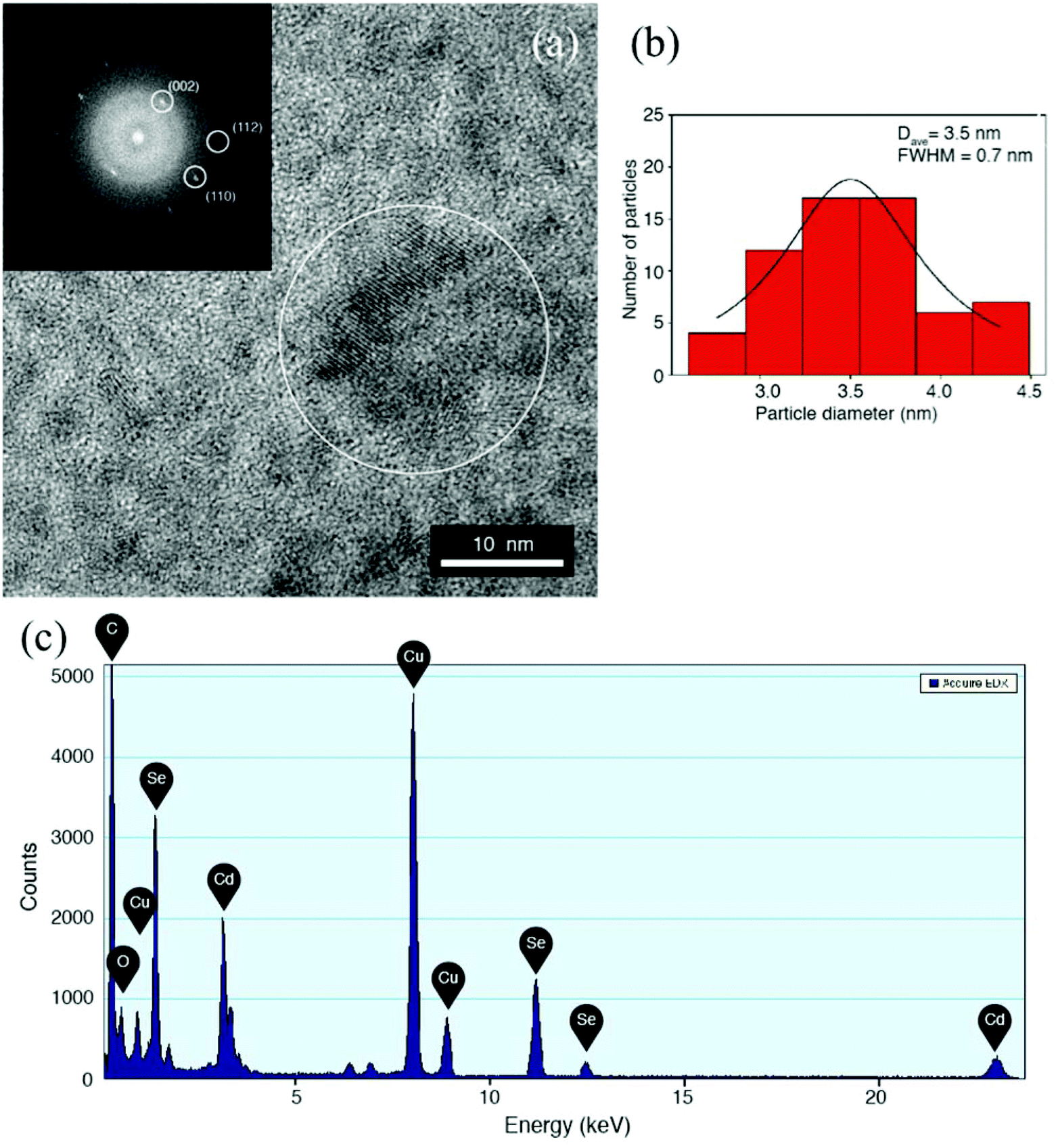 | ||
| Fig. 5 (a) High-resolution TEM image of QDs generated by thermal baking of the TPBI/precursor film at 160 °C for 15 minutes. (Inset) FFT of the highlighted area, showing lattice reflections from (002), (110) and (112) planes of CdSe crystal lattice. (b) Histogram of the particles diameter as obtained by the analysis of the TEM micrographs. (c) EDS spectrum for the film, showing Cd and Se presence (Cu originating from the TEM grid). | ||
Fig. 6a shows a typical topographic image of the nanocomposite films of TPBI and CdDMASe precursors before baking the sample obtained by AFM. The RMS roughness measured onto 10 × 10 μm2 area is about 57 nm as shown in the figure. This rather high value is due to the presence of isolated globular aggregates onto the surface. After baking the films at 160 °C for 15 minutes the RMS roughness reduces to 1.3 nm as shown in Fig. 6b. Baking at higher temperatures leads to higher RMS roughness of 4.3 nm as shown in Fig. 6c. From the AFM images it is not possible to observe the single QDs in the backed samples but we can gather information only about clusters. The cluster distribution in the baked samples resulted to be 61 ± 3.6 cluster per μm2 (each cluster is about 80 nm in size) and 40.6 ± 1.5 cluster per μm2 (each cluster is about 130 nm in size) at 160 °C and 170 °C respectively (Fig. 6b and c). These data suggest that the temperature rise induces the aggregation of QDs, because the cluster size increases from 80 to 130 nm and at the same time the surface coverage shifts from about 30% to 50%. These results are in correlation with the results obtained by TEM and PLQY measurements and suggest that QDs can be formed under different baking conditions but the nanoparticle aggregation takes place at higher temperatures with a consequent decrease in QD PLQY as it was previously observed. In comparison to our earlier published work21 where we used a polymer blended with this precursor, here we have shown that the thermolysis also works well with a small charge transporting molecule, and go on to demonstrate laser photo-patterning.
 | ||
| Fig. 6 AFM images of the TPBI/CdSe blends (a) before baking, (b) after baking at 160 °C for 15 minutes and (c) after baking at 170 °C for 15 minutes. The RMS reduces from 57 nm before baking to 1.3 nm after baking at 160 °C for 15 minutes. The RMS increases further at higher temperatures to 4.3 nm for baking at 170 °C for 15 minutes. | ||
Photo-patterning of nanocomposite films of TPBI and CdDMASe precursors
For photopatterning the samples were prepared in the same way as for photophysical studies. The laser treatment of the nanocomposite films was performed using a picosecond laser generating light at a wavelength of 266 nm which matches absorption of the precursor having the dominant absorption in the region of 250–280 nm. The first step was to explore the effect of the laser irradiation dose on the blend films. The effect of both pulse energy and number of pulses was explored by illuminating a grid of dots by increasing pulse energies (1 nJ to 15 nJ) in one direction and increasing number of pulses (20 to 10240) in the perpendicular direction. The resistance of the materials to the laser irradiation dose (damage, ablation, burning) was investigated to find the appropriate regime for laser patterning (without damage). The diameters of laser-modified spots on the material were measured by optical microscopy. Fig. 7a shows the fluorescence microscopy image of a sample where we have written a test grid in which the number of pulses changes along the x-axis and the pulse energy changes along the y-axis. The product of the number of pulses and the pulse energy gives the total laser irradiation dose. Fig. 7a illustrates clearly that at higher irradiation doses the film is destroyed. At lower intensity different colour intensities of light emission were observed by naked eye. This is interesting for its potential to allow laser writing of the colour of light emission. As the colour is directly related to the particle size, it also shows that the conditions of laser writing can control the particle size. The fluorescence emission was observed mainly around the center of the laser-irradiated spot. | ||
| Fig. 7 (a) Fluorescence microscopy image of the TPBI/CdDMASe precursor after laser irradiation by a grid of laser spots with distance between spots 50 μm, number of pulses on the x-axis and pulse energy on the y-axis; (b) laser scanning at different mean power settings, 100 kHz, 0.75 nm, hatch 5 μm; (c) LAMP logo, with laser parameters: 1.05 mW, 100 kHz, 10.5 nJ, 0.75 mm s−1, hatch 3 μm. | ||
Fig. 7b shows the stripes generated by laser scanning at different mean power settings of 100 kHz, 0.75 nm and 5 μm hatches. The highest and lowest intensities of irradiation lead to absence of fluorescence. This is because the highest intensity ablates the film, whilst the lowest intensity does not convert the precursor to nanoparticles. The intermediate intensities give strong fluorescence, further demonstrating the potential for laser writing. The threshold values for laser irradiation doses, which were able to induce modification of materials or damage of the films and materials, were estimated from Fig. 7a and b. This indicates that there is a processing window for laser patterning where material modification occurs below the film damage threshold. The fluorescence and absorption spectra were also recorded and results were similar to results obtained by thermal baking the samples. Using the optimized laser scanning parameters deduced from Fig. 7b, a moderate laser power of 1.05 mW was selected to write the LAMP project logo in a blend sample and the resulting fluorescence image is shown in Fig. 7c. The image scale bar is 100 μm. Here the mechanism of CdSe formation is due to the rise of temperature induced by laser pulse absorbed by precursors in the polymer blend. The temperature reached by the polymer blend can be estimated by simulation of heat transfer, considering the material parameter and is consistent with the baking conditions as discussed earlier. The intensity of coloring and yellow-red-brown color of the samples noticed by the naked eye were dependent also on the laser irradiation dose.
The laser-assisted synthesis of CdSe nanoparticles in solution recently reported by Lin et al.35 shows that nanoparticle formation is a function of the temperature and of the energy absorbed from the photons supplied to the solution by the laser. Fragouli et al.36 have shown that the laser wavelength in combination with the polymer matrix plays a crucial role in laser decomposition of a single source precursor, strongly affecting the optical properties of the resulting CdS QDs. Our results now show that the DLP technique is a convenient and flexible tool due to its path-directed and maskless fabrication process, providing a powerful new approach for patterning light-emitting materials on surfaces for applications in displays, lighting and sensing.
Conclusion
In summary, we have demonstrated laser writing of emissive QDs in a conjugated small molecule matrix using a picosecond laser. The dots form in situ from the action of the laser on the QD precursor. We have shown that conventionally used electron transport materials like TPBI in optoelectronic devices can be used together with single source precursors to form emissive QDs either by thermolysis or laser irradiation. Our results show that our in situ method of fabricating emissive QDs gives materials with reasonably high PLQY. We also demonstrated the use of time/temperature or irradiation time/laser power to achieve size (and spectroscopic) tuning of the final particles. The observed correlations between the QD size and laser process parameters illustrate the potential of the proposed QD formation technique to control organic/precursor composites for the production of light-emitting devices.Acknowledgements
We acknowledge financial support from the FP7 LAMP project “Laser Induced Synthesis of Polymeric Nanocomposite Materials and Development of Micro-patterned Hybrid Light Emitting Diodes (LED) and Transistors (LET)” (Grant No. 247928). AKB and IDWS also acknowledge financial support from the EPSRC Programme grant “Challenging the limits of photonics: Structured light” EP/J01771X/1. In addition IDWS acknowledges a Royal Society Wolfson Research Merit Award.Notes and references
- W. U. Huynh, J. J. Dittmer and A. P. Alivisatos, Science, 2002, 295, 2425–2427 CrossRef CAS PubMed.
- G. Yu and A. J. Heeger, J. Appl. Phys., 1995, 78, 4510–4515 CrossRef CAS PubMed.
- S. Coe, W.-K. Woo, M. Bawendi and V. Bulovic, Nature, 2002, 420, 800–803 CrossRef CAS PubMed.
- Y. Yuan, Q. Dong, B. Yang, F. Guo, Q. Zhang, M. Han and J. Huang, Sci. Rep., 2013, 3 CAS.
- S. H. Ko, I. Park, H. Pan, C. P. Grigoropoulos, A. P. Pisano, C. K. Luscombe and J. M. J. Fréchet, Nano Lett., 2007, 7, 1869–1877 CrossRef CAS PubMed.
- M. P. Aldred, A. E. A. Contoret, S. R. Farrar, S. M. Kelly, D. Mathieson, M. O'Neill, W. C. Tsoi and P. Vlachos, Adv. Mater., 2005, 17, 1368–1372 CrossRef CAS PubMed.
- J. C. Garno, Y. Yang, N. A. Amro, S. Cruchon-Dupeyrat, S. Chen and G.-Y. Liu, Nano Lett., 2003, 3, 389–395 CrossRef CAS.
- V. Strong, Y. Wang, A. Patatanyan, P. G. Whitten, G. M. Spinks, G. G. Wallace and R. B. Kaner, Nano Lett., 2011, 11, 3128–3135 CrossRef CAS PubMed.
- Y. Son, J. Yeo, H. Moon, T. W. Lim, S. Hong, K. H. Nam, S. Yoo, C. P. Grigoropoulos, D.-Y. Yang and S. H. Ko, Adv. Mater., 2011, 23, 3176–3181 CrossRef CAS PubMed.
- L. Cao, S. Yang, W. Gao, Z. Liu, Y. Gong, L. Ma, G. Shi, S. Lei, Y. Zhang, S. Zhang, R. Vajtai and P. M. Ajayan, Small, 2013, 9, 2905–2910 CrossRef CAS PubMed.
- M. Sakamoto, T. Tachikawa, M. Fujitsuka and T. Majima, Chem. Mater., 2008, 20, 2060–2062 CrossRef CAS.
- Z. B. Sun, X. Z. Dong, W. Q. Chen, S. Nakanishi, X. M. Duan and S. Kawata, Adv. Mater., 2008, 20, 914–919 CrossRef CAS PubMed.
- K. R. Justin Thomas, J. T. Lin, Y. T. Tao and C. W. Ko, J. Am. Chem. Soc., 2001, 123, 9404–9411 CrossRef PubMed.
- S. Ren, L.-Y. Chang, S.-K. Lim, J. Zhao, M. Smith, N. Zhao, V. Bulović, M. Bawendi and S. Gradečak, Nano Lett., 2011, 11, 3998–4002 CrossRef CAS PubMed.
- S. Yang, C.-F. Wang and S. Chen, J. Am. Chem. Soc., 2011, 133, 8412–8415 CrossRef CAS PubMed.
- M. Y. Odoi, N. I. Hammer, K. Sill, T. Emrick and M. D. Barnes, J. Am. Chem. Soc., 2006, 128, 3506–3507 CrossRef CAS PubMed.
- J. C. Ribierre, T. Aoyama, T. Muto and P. André, Org. Electron., 2011, 12, 1800–1805 CrossRef CAS PubMed.
- D. V. Talapin, J.-S. Lee, M. V. Kovalenko and E. V. Shevchenko, Chem. Rev., 2009, 110, 389–458 CrossRef PubMed.
- H. C. Leventis, S. P. King, A. Sudlow, M. S. Hill, K. C. Molloy and S. A. Haque, Nano Lett., 2010, 10, 1253–1258 CrossRef CAS PubMed.
- F. Antolini, T. Di Luccio, A. M. Laera, L. Mirenghi, E. Piscopiello, M. Re and L. Tapfer, Phys. Status Solidi B, 2007, 244, 2768–2781 CrossRef CAS PubMed.
- A. K. Bansal, F. Antolini, M. T. Sajjad, L. Stroea, R. Mazzaro, S. G. Ramkumar, K. J. Kass, S. Allard, U. Scherf and I. D. W. Samuel, Phys. Chem. Chem. Phys., 2014, 16, 9556–9564 RSC.
- V. Resta, A. M. Laera, A. Camposeo, E. Piscopiello, L. Persano, D. Pisignano and L. Tapfer, J. Phys. Chem. C, 2012, 116, 25119–25125 CAS.
- G. Kedarnath, S. Dey, V. K. Jain, G. K. Dey and B. Varghese, Polyhedron, 2006, 25, 2383–2391 CrossRef CAS PubMed.
- N. C. Greenham, I. D. W. Samuel, G. R. Hayes, R. T. Phillips, Y. A. R. R. Kessener, S. C. Moratti, A. B. Holmes and R. H. Friend, Chem. Phys. Lett., 1995, 241, 89–96 CrossRef CAS.
- M. A. Malik, M. Afzaal and P. O'Brien, Chem. Rev., 2010, 110, 4417–4446 CrossRef CAS PubMed.
- O. F. Z. Khan and P. O'Brien, Polyhedron, 1991, 10, 325–332 CrossRef.
- W. S. Rees and G. Kräuter, J. Mater. Res., 1996, 11, 3005–3016 CrossRef CAS.
- S. Dey, V. K. Jain, S. Chaudhury, A. Knoedler and W. Kaim, Polyhedron, 2003, 22, 489–491 CrossRef CAS.
- L. Stroea, A. K. Bansal, I. D. W. Samuel, S. Kowalski, S. Allard, U. Scherf, L. Ortolani, S. Cavallini, S. Toffanin and F. Antolini, Sci. Adv. Mater., 2015, 7, 1–14 CrossRef CAS PubMed.
- J. G. Brennan, T. Siegrist, P. J. Carroll, S. M. Stuczynski, P. Reynders, L. E. Brus and M. L. Steigerwald, Chem. Mater., 1990, 2, 403–409 CrossRef CAS.
- K. Osakada and T. Yamamoto, J. Chem. Soc., Chem. Commun., 1987, 1117–1118, 10.1039/C39870001117.
- P. Reiss, E. Couderc, J. De Girolamo and A. Pron, Nanoscale, 2011, 3, 446–489 RSC.
- Y. Park and R. C. Advincula, Chem. Mater., 2011, 23, 4273–4294 CrossRef CAS.
- A. M. Smith and S. Nie, Acc. Chem. Res., 2009, 43, 190–200 CrossRef PubMed.
- Y.-W. Lin, M.-M. Hsieh, C.-P. Liu and H.-T. Chang, Langmuir, 2004, 21, 728–734 CrossRef PubMed.
- D. Fragouli, P. P. Pompa, M. Kalyva, G. Caputo, L. Tapfer, R. Cingolani and A. Athanassiou, J. Phys. Chem. C, 2010, 114, 13985–13990 CAS.
| This journal is © The Royal Society of Chemistry 2015 |