
Manual assembly of nanocrystals for enhanced photoelectrochemical efficiency of hematite film†
Hyun Gil
Cha
,
Myung Jong
Kang
,
In Chul
Hwang
,
Hyunsung
Kim
*,
Kyung Byung
Yoon
and
Young Soo
Kang
*
Korea Center for Artificial Photosynthesis and Department of Chemistry, Sogang University, Seoul, 121-742, Korea. E-mail: kimhs@sogang.ac.kr; yskang@sogang.ac.kr
First published on 26th February 2015
Abstract
To improve the optoelectronic properties of hematite film as a photoanode, hematite film was orientated on the (012) plane by the secondary growth of organized microcrystals. The resultant film showed promising photoelectrochemical effects compared with a randomly oriented one, with a maximum photocurrent of 0.8 mA cm−2 at 1.23 V vs. RHE under the illumination of 1 sun.
Designing the morphology or exposed facets of photocatalyst crystals has received intense interest due to theoretical predictions that high energy facets show higher photocatalytic activity than low surface energy facets. Several groups have substantiated the above theoretical prediction by the successful synthesis of certain facet-exposed photocatalytic crystals, which were used to evaluate of the role of the crystal facet in a real photocatalyst reaction.1 In this regard, the morphology and the controlled crystal-facet synthesis of semiconductors for photocatalysts are becoming attractive issues, because of the enhanced or optimized photocatalytic properties obtained by tailoring the surface atomic structures.2,3 Several studies have extended this route to controlled crystal facet synthesis without a capping agent. For example, Lu et al. found that {001} facets of anatase TiO2 are much more reactive than {101} facets for H2 production,4 and Zhi et al. demonstrated that hematite nanorods with {110} facets are much more photoreactive than other facets such as {001} and {012} for the photodegradation of an organic dye.5
From the viewpoint of a photoelectrochemical cell (PEC) for utilizing solar light, photoanodes or photocathodes with a particular photoactive facet exposed are highly desirable. Although specific element doping has shown great potential in achieving high solar-energy conversion efficiency, an oriented thin film as a photoelectrode with a certain photoactive facet can be an alternative way to improve PEC efficiency by facilitating transport/collection of photo-generated electrons and holes based on anisotropic charge carrier mobility in hematite.
Hematite (α-Fe2O3),6 the most stable iron oxide, is non-toxic, abundant and low-cost, possessing n-type semiconducting properties under ambient conditions and a low band gap (∼2.1 eV)7 that allows for the absorption of a significant portion of the incident visible solar spectrum as well as sufficient chemical and photo-electrochemical (PEC) stability in alkaline aqueous electrolytes.8 Therefore, it is a potentially viable photoanode for use in solar water splitting, thereby producing oxygen. However, the reported efficiencies of hematite photoanodes are significantly lower than the predicted value due to low conductivity, short excited-state lifetimes (<10 ps),9 poor oxygen evolution reaction kinetics, and short hole diffusion lengths (2–4 nm).10
In this work, we report methods for the assembly of nano- and micro-sized crystals with plane orientation using straightforward manual assembly (rubbing method)11 and secondary growth12 of seed layers in a hydrothermal reaction via oriented attachment13 for the fabrication of transparent and plane oriented hematite film in FTO glass (F:SnO2 glass) (Fig. S1, ESI†).
Significantly, an unprecedented (012) plane oriented hematite film showed high PEC performance compared to a randomly oriented film without doping. The photocurrent onset potential of the (012) plane orientated hematite film shows a cathodic shift of ca. 0.1 V compared with the randomly orientated film, and achieves a maximum photocurrent density of 0.8 mA cm−2 at 1.23 V vs. RHE.
Theoretical calculations suggest that the Fe2O3 (001) and (012) surfaces have similar surface energies, with the energy of the (012) surface slightly lower by ∼0.1 J m−2 in hematite, which can contribute to the selection of a synthetic method to obtain the largest exposed surface area of the highest photoactive facet.14
Monodisperse hematite pseudocubes (Fig. 1(a-1) and Fig. S2, ESI†) with a diameter of ∼550 nm were prepared as the building blocks for the orientated crystals by a simple hydrothermal reaction according to modified previous reports.15 From the cross-sectional TEM image and SAED pattern in Fig. S2(b and c) (ESI†), the hematite crystal was bound entirely by {012} facets, because it consisted of rod-shaped subunits by orientated attachment in both longitudinal and lateral directions of the rod-shaped subunits. The crystal structure of the synthesized hematite crystals has been characterized as pure α-Fe2O3 phase (JCPDS card no. 33-0664) by analysis of X-ray diffraction pattern (XRD) in Fig. 1(a). FTO glass was spin-coated with polyethyleneimine (PEI) in ethanol; hematite crystals were then rubbed gently with a finger on the PEI coated substrate. Hematite crystals were formed by hydrogen bonding among the two layers of hematite hydroxyl groups and PEI on the FTO glass.
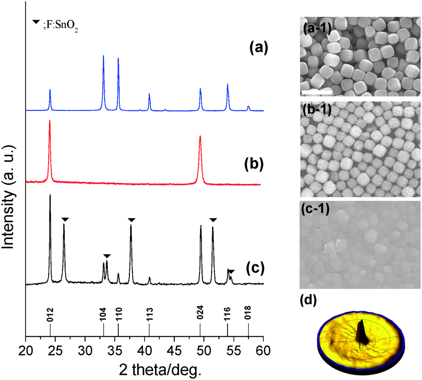 | ||
| Fig. 1 XRD patterns and SEM images of hematite crystals (a, a-1), arranged hematite crystals on an amorphous glass substrate (b, b-1) and secondary grown hematite continuous film on the FTO glass (c, c-1), grown at 150 °C for 4 h and annealed at 500 °C for 3 h. (d) (012) XRD pole figure of secondary grown hematite continuous film. All scale bars are 1 μm. | ||
PEI should be removed by calcination at 500 °C for 3 h,16 in order not only to improve adhesion between the hematite crystals and the FTO glass but also to remove ineffective ones which would hinder charge transportation.17 After the rubbing process, diffraction lines appeared only at 2θ values of 24.15° and 49.46°, corresponding to the (012) and (012) plane of the crystals as shown by analysis of the XRD pattern in Fig. 1(b). This means that the film was orientated along the (012) plane. Calcined hematite crystals on FTO glass readily allow continuous (012) plane growth with gaps filled between crystals and the surface of FTO glass by secondary growth through orientated attachment.15 The SEM image and XRD pattern of hematite films after secondary growth are shown in Fig. 1(c, c-1). XRD patterns of secondary grown hematite film with different reaction times show that the intensities of the (012) and (024) peaks gradually increase, from 1.1 to 2.85 times higher, with increasing reaction time (Fig. S3(a), ESI†), with respect to the intensity of the dominant peak at 26.60° from the FTO glass substrate, although other peaks from hematite were found due to the roughness of the FTO glass. This implies that the gap filling among hematite crystals occurs along with an increase in film thickness, with maintenance of the (012) plane orientation, after secondary growth. The thickness of hematite film after secondary growth for 4 h was ∼750–800 nm as shown in Fig. 2(a).
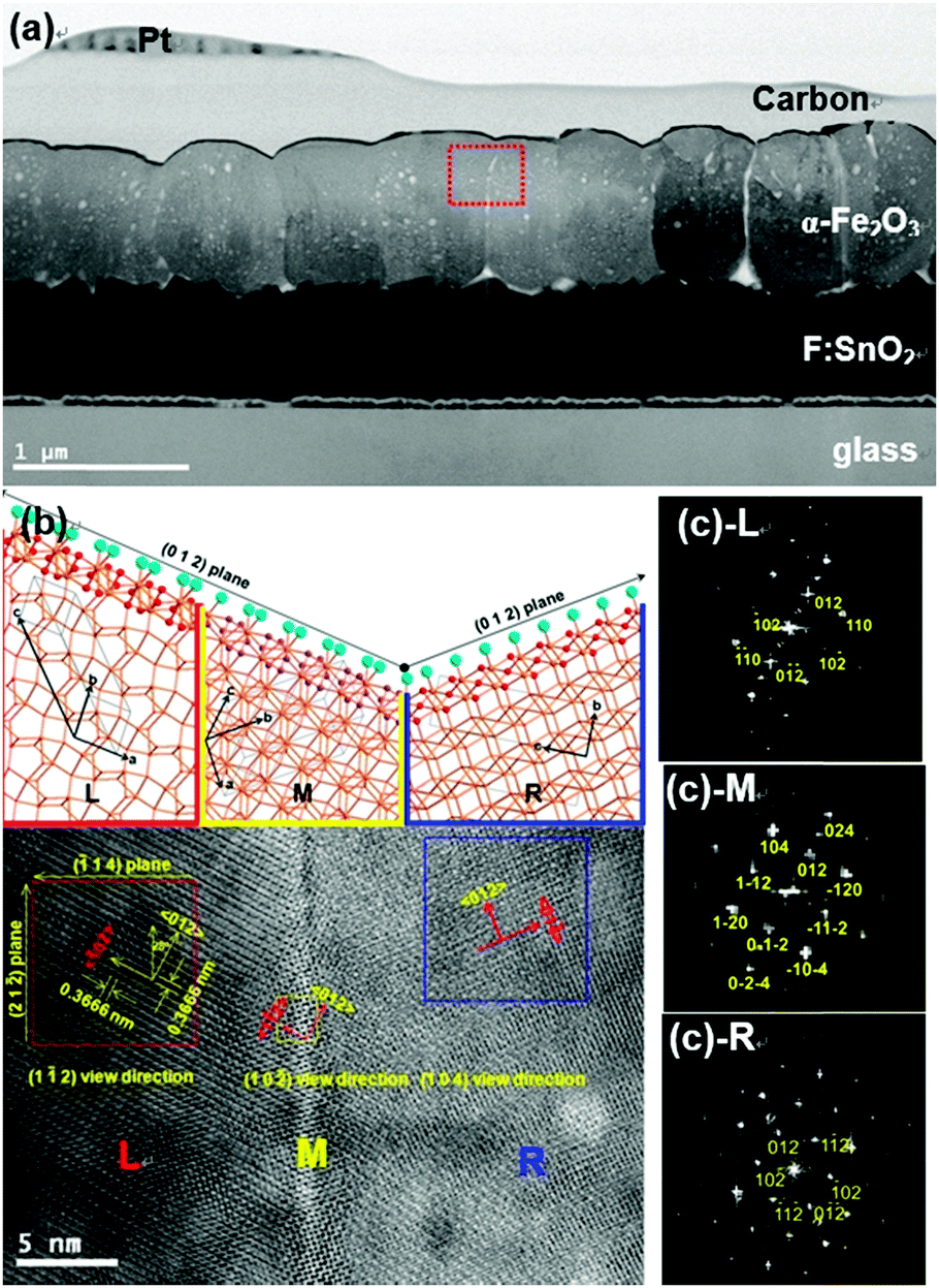 | ||
| Fig. 2 (a) Cross-sectional TEM image of a piece of the (012) plane orientated hematite film on the FTO, (b) HRTEM image and (c) fast-Fourier transformation (FFT) diffraction patterns of selected square areas L, M, and R-zone (L; left; M; middle; R; right). The atomic network structure shown is the introduced lattice structure and orientation from (b) and demonstrates hydroxyl groups on the (012)-plane surface in hematite film. The orange, red, and blue spheres are representative of iron atoms, oxygen atoms, and the hydroxyl group, respectively. | ||
The XRD pole figure is a well-established technique to provide crystal growth orientation on the surface (Fig. 1(d) and Fig. S4, ESI†). The (012) XRD pole figure reveals maximum intensity at 0° tilt angle. This indicates that most of the (012) planes are parallel to the substrate. In the case of the (104) pole figure, no definite features are observed, indicating the absence of the (104) plane parallel to the substrate. As expected, the plane without one-axis growth orientation gives an off-peak intensity, which is invariant of the tilt angle. On the other hand, a ring pattern is observed at around 46.7°, which is attributed to the planes with an interfacial angle between the (012) and (104) planes. Therefore, pole figure results have shown that the obtained secondary grown hematite film has a (012) plane orientation. The randomly oriented hematite film showed a dominant orientation along the (104) plane (Fig. S5, ESI†).
A detailed crystallographic relationship was revealed by HRTEM and related fast-Fourier transformation (FFT) electron diffraction patterns (EDP). A TEM image showed a piece of hematite continuous film with individual (012) plane orientated crystals, which was located at a different position on the rough FTO glass (Fig. 2(a)). The HRTEM images shown in Fig. 2(b), taken from the red, orange, and blue square areas, and individual SAED patterns, contain parts along [1−12] (L), [10−2] (M), and [104] (R) zone axis, respectively (Fig. 2(b) and (c)). The discontinuous lattice plane with left and right sides present among the lattice fringes suggests the growth of film initiated the arrangement of hematite crystals, which located on the rough surface of FTO glass. The growth direction of all positions is along their 〈012〉 axis.
The (012) plane orientated film possessed short Fe–O bond lengths, ∼0.19 nm (Fig. 2(b)), which results in the improvement of charge transport along the (012) plane.18 In addition, the well-connected continuous crystal film enhanced inter-particle electron transportation and crystal structure deformation.19 The randomly orientated hematite film of ca. 750 nm thickness is shown in Fig. S6 (ESI†). The SAED patterns of the crystal and interface between crystals of the random film are consistent with single and poly-crystal features, respectively. It is a direct indication of recombination loss of photogenerated electrons in the photoanode, hindering electron transportation from the electrode to back contact, because recombination mainly occurs due to mismatched interfaces in the film such as internal defects.
In the Fe 2p and O 1s core-level X-ray photoelectron spectroscopy (XPS) spectra of the hematite crystals and oriented hematite film (Fig. S7(a and b), ESI†), the Fe 2p3/2 peaks appear at a binding energy of about 711.4 eV, which is the typical value for Fe3+ in α-Fe2O3. Instead of this, we observed a value of 708.54 eV, corresponding to the peak intensity of the difference between the oriented hematite film and the randomly oriented hematite crystals. This revealed that there is evidence for an additional Fe species, which has oxygen deficiencies at a binding energy of ∼708 eV, on the (012) plane oriented hematite continuous film.20 This is also reflected in the O 1s spectra of both samples (Fig. S12(c), ESI†), which show three different types of peaks, corresponding to structural O2−, water (H2O), and a broad peak consisting of OH or O–C groups. We observed surface OH groups on the (012) oriented continuous film at ∼299 eV, which bonded with the oxygen deficient Fe species with relatively short bond lengths between the Fe and O atoms.
A UV-vis study is a facile method to characterize the thickness of a hematite film. Therefore, random and (012) plane orientated hematite films were measured and the results are shown in Fig. S8 (ESI†). The absorption is similar for both the random and (012) plane orientated samples, which suggests that the thicknesses of hematite are similar. Moreover, higher magnification TEM images were also measured and showed continuous film formation (see Fig. S6, ESI†).
The photoelectrochemical performances of random and (012) plane orientated hematite were first compared by measuring a photocurrent density–potential (J–V) plot under AM 1.5G (100 mW cm−2) illumination in 1 M NaOH (pH 13.6). Fig. 3(a) shows that both random and (012) plane orientated hematite electrodes are n-type and generate anodic photocurrents by the consumption of photoinduced holes for water oxidation, serving as photoanodes. While the random orientated hematite photoanode shows a photocurrent density of less than 0.2 mA cm−2 at 1.23 V vs. RHE, the (012) plane orientated hematite film showed drastically enhanced performance and generated photocurrent densities of almost 1 mA cm−2 at a potential of 1.23 V vs. RHE, as shown in Fig. 3(b). Compared to the randomly orientated electrode, the (012) plane orientated hematite film showed a significantly shifted cathodic potential of about 0.1 VRHE. In addition, the photocurrent density was increased about 4 times. J–V curves of the films grown for different secondary growth times under light illumination were recorded (Fig. S9, ESI†). The photocurrent values were enhanced with increasing growth time, which is related to the extent of gap filling among crystals. This enhancement can be attributed to the increased charge transport in the plane orientated film. We note that the arranged hematite crystal photoelectrodes without secondary growth did not show any photovoltaic effect (Fig. S9, ESI†). The highest photocurrent density was obtained from the secondary grown hematite film for 4 h, being 0.8 mA cm−2 at 1.23 VRHE, and this photocurrent density value lasted over 2 hours (Fig. 3 and Fig. S10, ESI†). When the secondary growth time exceeds 4 h, the photocurrent density decreases by more than 50% due to the formation of small particles of mismatched crystals on the hematite film. The junction of main hematite crystal and these small particles possibly generates electron trap sites and results in the reduction of the photovoltaic effect (Fig. S11, ESI†).
 | ||
| Fig. 3 Photocurrent vs. potential curves and transient photocurrent of the (012) plane and random orientated hematite continuous films in 1 M NaOH (pH 13.6) when the light is on and off at a potential of 1.23 VRHE. | ||
Electrochemical impedance spectroscopy (EIS) was used to investigate the charge transfer process at the semiconductor–electrolyte interface, as shown in Fig. S12 (ESI†). We measured the EIS spectra of the (012) plane orientated hematite film at close to the onset potential for water oxidation. From the results of the EIS spectra at −0.2 VAg/AgCl under dark and light illumination in Fig. S12 (ESI†), the radii of low frequency response become smaller after (012) orientation in the hematite film, compared with the randomly orientated film in dark conditions and light illumination conditions. This means that the interface charge transfer rate increases in the (012) orientated hematite film. The enhanced charge transfer rate results from one-axis orientated crystallinity, due to enhanced electron mobility, inter-particle electric connectivity, and low recombination loss of electrons for water oxidation.
In summary, a novel process for the formation of (012) plane-oriented hematite film has been achieved by the assembly of pseudocubes with {012} facets and a secondary growth process. Compared with the pristine hematite photoanode, the obtained (012) plane-oriented continuous hematite film shows an increased photocurrent density of 0.8 mA cm−2 at 1.23 V vs. RHE without the incorporation of dopants or an oxygen evolution catalyst. The enhancement of photocurrent density is attributed to a high electron/hole diffusivity between the Fe and O atoms and interparticle electronic connectivity. This allows low energy consumption for water oxidation. This work demonstrates a simple and effective method for the largest exposure of the highest photoactive (012) plane as a photoanode for use in PEC water oxidation.
This work was supported by the Korea Center for Artificial Photosynthesis (KCAP) located in Sogang University funded by the Minister of Science, ICT and Future Planning (MSIP) through the National Research Foundation of Korea (No. 2009-0093885) and the Brain Korea 21 Plus Project 2014.
Notes and references
- Y. Bi, S. Ouyang, N. Umezawa, J. Cao and J. Ye, J. Am. Chem. Soc., 2011, 133, 6490 CrossRef CAS PubMed.
- Y. Qiu, S. Leung, Q. Zhang, B. Hua, Q. Lin, Z. Wei, K. Tsui, Y. Zhang, S. Yang and Z. Fan, Nano Lett., 2014, 14, 2123–2129 CrossRef CAS PubMed.
- J. Li, Y. Qiu, Z. Wei, Q. Lin, Q. Zhang, K. Yan, H. Chen, S. Xiao, Z. Fan and S. Yang, Energy Environ. Sci., 2014, 7, 3651–3658 CAS.
- H. Yang, C. Sun, S. Qiao, J. Zou, G. Liu, S. Smith, H. Cheng and G. Lu, Nature, 2008, 453, 638 CrossRef CAS PubMed.
- X. Zhou, J. Lan, G. Liu, K. Deng, Y. Yang, G. Nie, J. Yu and L. Zhi, Angew. Chem., 2012, 51, 178 CrossRef CAS PubMed.
- R. M. Cornell and U. Schwertmann, The Iron Oxides: Structure, Properties, Reactions, Occurrences, and Uses, Wiley-VCH, Weinheim, 2nd edn, 2003 Search PubMed.
- (a) J. H. Kennedy and K. W. Frese, J. Electrochem. Soc., 1978, 125, 723 CrossRef CAS; (b) M. P. Dareedwards, J. B. Goodenough, A. Hamnett and P. R. Trevellick, J. Chem. Soc., Faraday Trans., 1983, 79, 2027 RSC; (c) Z. Sun, H. Yuan, Z. Liu, B. Han and X. Zhang, Adv. Mater., 2005, 17, 2993 CrossRef CAS; (d) A. B. Murphy, P. R. F. Barnes, L. K. Randeniya, I. C. Plumb, I. E. Grey, M. D. Horne and J. A. Lasscock, Int. J. Hydrogen Energy, 2006, 31, 1999 CrossRef CAS; (e) H. G. Cha, J. Song, H. S. Kim, W. Shin, K. B. Yoon and Y. S. Kang, Chem. Commun., 2011, 47, 2441 RSC.
- R. L. Spray, K. J. McDonald and K. S. Choi, J. Phys. Chem. C, 2011, 115, 3497 CAS.
- (a) A. G. Joly, J. R. Williams, S. A. Chambers, G. Xiong, W. P. Hess and D. M. Laman, J. Appl. Phys., 2006, 99, 53521 CrossRef; (b) N. J. Cherepy, D. B. Liston, J. A. Lovejoy, H. M. Deng and J. Z. Zhang, J. Phys. Chem. B, 1998, 102, 770 CrossRef CAS.
- O. Khaselev and J. A. Turner, Science, 1998, 280, 425 CrossRef CAS PubMed.
- J. S. Lee, J. H. Kim, Y. J. Lee, N. C. Jeong and K. B. Yoon, Angew. Chem., Int. Ed., 2007, 46, 3087 CrossRef CAS PubMed.
- Z. Lai, G. Bonilla, I. Diaz, J. G. Nery, K. Sujaoti, M. A. Amat, E. Kokkoli, O. Terasaki, R. W. Thompson, M. Tsapatsis and D. G. Vlachos, Science, 2003, 300, 456 CAS.
- J. S. Chun, T. Zhu, C. M. Li and X. W. Lou, Angew. Chem., Int. Ed., 2011, 50, 650 CrossRef PubMed.
- P. Liao and E. A. Carter, J. Mater. Chem., 2010, 20, 6703 RSC.
- H. Colfen and M. Antonietti, Angew. Chem., Int. Ed., 2005, 44, 5576 CrossRef PubMed.
- N. N. Khanh and K. B. Yoon, J. Am. Chem. Soc., 2009, 131, 14228 CrossRef CAS PubMed.
- M. G. Kim, J. W. Hennek, H. S. Kim, M. G. Kanatzidis, A. Facchetti and T. J. Marks, J. Am. Chem. Soc., 2012, 134, 11583 CrossRef CAS PubMed.
- N. Iordanova, M. Dupuis and K. M. Rosso, J. Chem. Phys., 2005, 122, 144305 CrossRef CAS PubMed.
- S. Saretni-Yarahmadi, K. G. U. Wijayantha, A. A. Tahir and B. Vaidhyanathan, J. Phys. Chem. C, 2009, 113, 4768 Search PubMed.
- G. Wang, Y. Ling, D. A. Wheeler, K. E. N. Geroge, K. Horsley, C. Heske, J. Z. Zhang and Y. Li, Nano Lett., 2011, 11, 3503–3509 CrossRef CAS PubMed.
Footnote |
| † Electronic supplementary information (ESI) available: Experimental details, TEM images, X-ray diffraction patterns, X-ray photoelectron spectroscopy, UV-Vis spectroscopy and Nyquist plots are provided. See DOI: 10.1039/c5cc00200a |
| This journal is © The Royal Society of Chemistry 2015 |