
 Open Access Article
 This Open Access Article is licensed under a Creative Commons Attribution-Non Commercial 3.0 Unported Licence
Enhancing interfacial charge transfer in mesoporous MoS2/CdS nanojunction architectures for highly efficient visible-light photocatalytic water splitting†
Chrysanthi
Patriarchea
,
Ioannis
Vamvasakis
,
Eirini D.
Koutsouroubi
and
Gerasimos S.
Armatas
 *
*
Department of Materials Science and Technology, University of Crete, Heraklion 70013, Greece. E-mail: garmatas@materials.uoc.gr
First published on 23rd December 2021
Abstract
Modulating the heterojunction interfaces at the nanoscale is paramount to developing effective photocatalysts. Nanodimensional heterostructures, essentially, expose a large fraction of active edge sites, which, along with excellent electronic communication, can result in high solar energy to chemical fuel conversion efficiencies. In this work, mesoporous heterojunction architectures made of ultrasmall MoS2 nanolayers (ca. 10–15 nm in lateral size) and sub 5 nm sized CdS nanocrystals have been prepared through a polymer-templated oxidative aggregation of CdS nanocrystals followed by a wet-chemical deposition of exfoliated MoS2 nanosheets on the CdS surface. Thorough chemical, morphological and structural investigations by electron microprobe analysis, X-ray diffraction, electron microscopy, X-ray photoelectron spectroscopy and N2 physisorption prove that the MoS2-modified CdS nanocatalysts are composed of a porous network of connected cubic CdS nanocrystals and 2H-phase MoS2 nanosheets and possess a high internal BET surface area (ca. 159–225 m2 g−1) and uniform pores (ca. 6–9 nm in diameter). Photocatalytic studies coupled with UV–vis/NIR, photoluminescence and electrochemical impedance spectroscopy measurements indicate that the nanoscale MoS2/CdS junctions provide more efficient electronic connectivity and charge carrier dissociation across the catalyst interfaces, resulting in a remarkable enhancement in the photocatalytic H2 production activity. The optimized MoS2/CdS catalyst at 20 wt% MoS2 content achieves a H2 production rate up to ∼0.4 mmol h−1 (or ∼19 mmol h−1 g−1 mass activity) with remarkable stability under visible light irradiation, corresponding to an overall 6.7× enhancement of H2 generation efficiency relative to the unmodified CdS. We also obtained an apparent quantum yield (AQY) of 51.2% for the hydrogen generation reaction using monochromatic light of 420 nm.
1. Introduction
Over the last few years, various renewable technologies have been used to effectively produce chemical fuels, such as hydrogen which is a promising alternative target for clean chemical energy source.1,2 Among them, solar hydrogen production by water-splitting photocatalysis has emerged as a particularly propitious approach because of the low cost, easy maintenance and environmental effectiveness.3 Thus far, a great variety of semiconducting materials, including metal oxides4 and sulfides,5,6 have been applied for catalytic hydrogen fuel generation. These materials satisfy the most important criteria of effective photocatalysts, such as substantial photon absorption (bandgap energy ∼2–2.8 eV) and favourable reduction and oxidation band positions.7–9 Metal sulfides, especially CdS, have been extensively studied due to their narrow bandgap (ca. 2.3–2.6 eV) and high negative conduction band (CB) level relative to the thermodynamic H+ reduction potential (−0.41 V, pH 7).10–12 However, the practical use of these materials is still plagued by photochemical corrosion and low photon-to-hydrogen conversion efficiency. To improve the photocatalytic activity of CdS, various strategies have been developed, including heterojunctions, core–shell structures, doping with metal or non-metal elements and loading of co-catalysts. For example, numerous reports have shown that electron-accepting co-catalysts, such as noble metals Pd and Pt on a CdS support, can mitigate charge recombination and thus accelerate the surface reaction for hydrogen evolution.13,14 Moreover, considering the high cost and limited availability of noble metals, inexpensive Earth-abundant metal-based co-catalysts have been recently examined.15,16After the revolution of graphene, transition metal dichalcogenides (TMDs), with the formula MX2 where M is Mo, W, etc. and X is S, Se, and Te, have also received attention as ideal co-catalysts for the photocatalytic H2 evolution reaction.17 Among TMDs, 2D molybdenum disulfide (MoS2), consisting of stacked S–Mo–S layers weakly bonded by van der Waals forces, has attracted significant attention owing to the low cost and excellent optical, physical and electronic properties.18 In the bulk or multilayer form, MoS2 has an indirect energy gap of about 1.3 eV, which transitions to a direct gap of 1.9 eV for a single monolayer. Besides the thermodynamically stable hexagonal 2H phase (semiconducting phase), MoS2 also adopts two metastable phases, that is, the rhombohedral 3R (semiconducting phase) and trigonal 1T (metallic phase) structure.19 Among these polytypes, 2H-MoS2 although exhibits lower mobility for transporting charge carriers than the metallic 1T-MoS2, shows better stability and interesting semiconducting properties that are useful for applications in light energy conversion and opto-electronics.20 Also, the 2H phase of MoS2 can exhibit better photocatalytic activities than the semiconducting 3R counterpart due to the unexfoliated structure of 3R-MoS2. In particular, the three-layered (3R) MoS2 form adopts a relatively more stable stacking structure between the S–Mo–S layers, which can result in lower accessibility of the reactants to the interlayer active sites.21 For this purpose, considering the semiconducting properties of MoS2, there have been extensive studies on various heterostructures using 2H-MoS2 as the co-catalyst for improved H2 production yield.22,23 For instance, Zhang et al. demonstrated the selective growth of single-layer MoS2 nanoflakes, with a 4–10 nm lateral size, on the Cd-rich (0001) surface of wurtzite CdS particles.24 This catalyst was reported to undergo photocatalytic reduction of water in the presence of lactic acid as the hole scavenger, yielding a H2 evolution rate of 1.47 mmol h−1 g−1. Song's group successfully prepared a 2D/2D heterojunction by assembling ultrathin MoS2 sheets and exfoliated CdS nanolayers through an adsorption–calcination process.25 They found that the optimal photocatalyst presented a maximum photocatalytic H2 production activity of 18.43 mmol h−1 g−1. More recently, Fujishima and coworkers coupled 2D MoS2 thin sheets as H2 evolution catalysts with CdS microspheres by a template-free solvothermal method.26 The nanostructured core–shell CdS@MoS2 particles showed high carrier transport efficiency and a remarkable H2 production activity of 4.16 mmol h−1 g−1 under natural solar light.
In the previous work, we have described the synthesis of mesoporous networks of small-sized CdS nanocrystals (NCs) through a polymer-assisted self-assembly method.27 These materials compared to the isolated nanoparticles and conventional porous solids have shown adequate photocatalytic properties, which resulted from the strong electronic communication between the constituent nanoparticles and the large exposed surface area of the assembled structure. Such CdS NC-linked structures combine a number of interesting features, such as a 3D open-pore structure, high internal surface area, visible light absorption and excellent structural stability.28 In this study, we report the synthesis of new high surface-area mesoporous frameworks consisting of CdS NCs (ca. 4–5 nm in diameter) and exfoliated 2H-MoS2 nanosheets (NSs) with an ultrasmall lateral size (ca. 10–15 nm) and evaluate their performance as catalysts for water splitting and H2 evolution under visible light. The 2D/3D MoS2/CdS nano-heterostructures with various loadings of MoS2 NSs, namely from 5 to 25 wt%, were synthesized through a facile deposition method. By using a combination of spectroscopic and electrochemical techniques, we provide an in-depth understanding of the structural, electronic and photochemical characteristics of the obtained catalysts. We demonstrate that the nanoscale dimension of the MoS2/CdS contacts minimizes electron–hole recombination and increases the electron density and mobility at the MoS2/CdS junction, yielding accelerated water reduction kinetics. Owing to these characteristics, the optimized catalyst with 20 wt% MoS2 NSs exhibits a significant enhancement of the photocatalytic activity, yielding an apparent quantum yield (AQY) of 51.2% for H2 evolution at 420 nm, a record efficiency for MoS2-modified CdS photocatalysts, to the best of our knowledge.
2. Experimental section
2.1 Synthesis of catalysts
For comparison purposes, MoS2 microflakes were also synthesized following a similar procedure, but using (NH4)6Mo7O24·4H2O (0.0275 mmol) as the Mo source.
![[thin space (1/6-em)]](https://www.rsc.org/images/entities/char_2009.gif) :isopropanol (IPA) solution (2:1 v/v, 30 mL) in a 50 mL beaker. The suspension was ultrasonicated for 2 h until a homogeneous black solution of exfoliated MoS2 NSs was formed. In a separate vial, mesoporous CdS NCAs (80 mg) were dispersed in a H2O:IPA solution (2:1 v/v, 5 mL) under vigorous stirring at RT. Finally, the suspension of exfoliated MoS2 NSs was added gradually to the CdS NCA dispersion and the resulting green mixture was left under stirring and low heat (50–60 °C) for slow evaporation of the solvents. The respective 5, 10, 15 and 25 wt% MoS2-modified CdS samples were synthesized following a similar procedure using the stoichiometric amount of MoS2 NSs for each case.
:isopropanol (IPA) solution (2:1 v/v, 30 mL) in a 50 mL beaker. The suspension was ultrasonicated for 2 h until a homogeneous black solution of exfoliated MoS2 NSs was formed. In a separate vial, mesoporous CdS NCAs (80 mg) were dispersed in a H2O:IPA solution (2:1 v/v, 5 mL) under vigorous stirring at RT. Finally, the suspension of exfoliated MoS2 NSs was added gradually to the CdS NCA dispersion and the resulting green mixture was left under stirring and low heat (50–60 °C) for slow evaporation of the solvents. The respective 5, 10, 15 and 25 wt% MoS2-modified CdS samples were synthesized following a similar procedure using the stoichiometric amount of MoS2 NSs for each case.
A bulk-like MoS2-modified CdS catalyst (designated as 20-MoS2/CdS_b) was also prepared by depositing 20 wt% of MoS2 microflakes on the surface of mesoporous CdS.
2.2 Photocatalytic water splitting study
The photocatalytic H2 evolution experiments were performed in an air-tight Pyrex glass cell with 20 mg of catalyst suspended in 20 mL of aqueous solution containing 0.25 M Na2SO3 and 0.35 M Na2S (except otherwise noted). Before irradiation, the suspension was bubbled with argon for 40 min. The reactor was illuminated using a 300 W Xe lamp (Variac Cermax) with a UV-cutoff filter (λ ≥ 420 nm) and the reaction temperature was thermostated to 20 ± 2 °C by a water-cooling system. During the experiment, 100 μL of gas was collected from the reactor's headspace and the generated H2 was measured using a gas chromatograph (Shimadzu GC-2014, TCD, with Ar as the carrier gas).The apparent quantum yield (AQY) was estimated by measuring the amount of hydrogen evolved at λ = 420 ± 10 nm irradiation wavelength, according to the following equation:

The intensity of light was measured using a StarLite power meter equipped with a FL400A-BB-50 thermal sensor (Ophir Optronics Ltd).
2.3 Characterization methods
X-Ray diffraction was performed on a Panalytical X'pert Pro MPD instrument with Cu-Kα radiation (λ = 1.5418 Å), operated at 45 kV and 40 mA. Energy-dispersive X-ray spectroscopy was performed on a JEOL JSM 6390 LV scanning electron microscope (SEM) equipped with an Oxford INCA PentaFETx3 detector (Oxfordshire, UK). For EDS analysis, because of the overlap of Mo-Lα and S-Kα lines, the samples were annealed at 800 °C in air for 3 h in order to detect the Mo:Cd atomic ratios, and the measurements were performed on at least five different regions of each sample using 20 kV acceleration voltage and 100 s accumulation time. Transmission electron microscopy measurements were performed with a JEOL JEM-2100 instrument (LaB6 filament) operating at 200 kV. The samples were prepared by dispersing fine powders in ethanol using sonication and then drop-casting on a holey carbon-coated Cu grid. X-ray photoelectron spectroscopy (XPS) was conducted on a SPECS spectrometer using a Phoibos 100 1D-DLD electron analyzer and Al Kα radiation as the energy source (1486.6 eV). Binding energy values were corrected with reference to the C 1s (284.8 eV) signal of adventitious carbon. UV–vis/near IR diffusion reflectance spectra were recorded with a Shimadzu UV-2600 spectrophotometer, using BaSO4 powder as a 100% reflectance reference. The diffuse reflectance data were transformed with the Kubelka–Munk function [α/S = (1 − R)2/(2R), where R is the measured reflectance and α and S are the absorption and scattering coefficients, respectively] into absorption spectra. N2 adsorption–desorption isotherms were obtained at −196 °C with a Quantachrome NOVA 3200e system. Prior to analysis the samples were heated at 80 °C under low pressure (<10−5 Torr) to remove residual solvents and water. The surface areas were determined from the adsorption data (P/P0 range 0.04–0.22) using the Brunauer–Emmett–Teller (BET) method, and the total pore volumes were calculated from the adsorbed N2 amount at P/P0 = 0.98. The pore size distribution plots were calculated from the absorption data using the non-local density functional theory (NLDFT) fitting model. Room temperature photoluminescence and decay curve analysis were performed with an Edinburgh FS5 spectrofluorometer.
2.4 Electrochemical measurements
Mott–Schottky plots, Nyquist plots and current–voltage (J–V) curves were measured in a 0.5 M Na2SO4 electrolyte (pH = 7) using a single-channel potentiostat–galvanostat (Princeton Applied Research VersaSTAT 4) equipped with a three-electrode cell, consisting of a sample-coated FTO working electrode, an Ag/AgCl (saturated KCl) reference electrode, and a Pt-wire counter electrode. The working electrodes were prepared as follows: 10 mg of each sample were dispersed in a 2-propanol/DI water solution (1:2 v/v, 1 mL). Then, 20 μL Nafion solution (5 wt%) was added and the mixture was ultrasonicated for 15 min and left under stirring for 24 h. When a uniform suspension was formed, 100 μL of the solution was dropped on a fluorinated tin oxide (FTO, 10 Ω sq−1) substrate (effective surface 1 cm2) and the film was dried under heat at 40–50 °C for 1 h.
The space-charge capacitance (Csc) of the semiconductor/electrolyte interface was measured at 1 kHz, with 10 mV AC voltage amplitude and the obtained flat-band potentials were converted to the reversible hydrogen electrode (RHE) scale using the equation: ERHE = EAg/AgCl + 0.197 V, where ERHE is the potential in the RHE scale and EAg/AgCl is the measured potential in the Ag/AgCl scale.
The donor density (ND) of the as-prepared materials was calculated according to the Mott–Schottky equation: ND = Csc2·2·(E − EFB)/ε·ε0·e0, where, CSC is the space charge capacitance, EFB is the flat band potential, E is the applied potential, ND is the donor density of the electrode material, ε is the dielectric constant (8.9 for CdS), ε0 is the vacuum permittivity (8.8542 × 10⁻¹⁴ F cm−1), e0 is the elementary charge (1.602 × 10⁻¹⁹ C) and the term (E − EFB)·CSC2 is the reciprocal of the slope of the Mott–Schottky plot.
For Nyquist plots, the current output was recorded between 1 Hz and 1 MHz with a 10 mV AC perturbation, under open-circuit potential. The EIS data were fitted to an equivalent circuit model using ZView Software.
3. Results and discussion
3.1 Materials synthesis and characterization
Porous networks of connected CdS NCs and 2H-MoS2 NSs were produced using a polymer-templated oxidative aggregating method followed by a wet-chemical deposition process. Initially, 2D nanolayers of 2H-MoS2 were prepared through a hydrothermal sulfurization reaction, using Na7[PMo11O39] and thioacetamide (CH3CSNH2) as the Mo and S source, respectively.31 After annealing to a certain temperature, thioacetamide begins to decompose and evolve H2S that is capable of transforming MoOxn− species into MoS2. The X-ray diffraction (XRD) pattern of as-made MoS2 NSs, in Fig. S1,† indicates the successful chemical transformation of phosphomolybdate clusters into MoS2 under our liquid-phase conditions; all the diffraction peaks can be assigned to the hexagonal (2H) structure of MoS2. Besides, the broadened XRD diffractions point to the nanoscale dimension of the MoS2 layers. Nanoporous networks of CdS NC assemblies (NCAs) were prepared based on a method described in a recent study, which involves the oxidative coupling of thiol-capped CdS nanoparticles with the assistance of a tri-block copolymer (Pluronic F-127) surfactant. MoS2 modification of the mesoporous CdS structure was realized by depositing the liquid exfoliated MoS2 NSs onto the surface of CdS NCAs. Following this process, several n-MoS2/CdS NCAs with different compositions of grafted MoS2, namely n = 5, 10, 15, 20 and 25 wt%, were prepared. The Mo/Cd atomic ratios of the as-prepared materials were determined by elemental analysis with energy dispersive X-ray spectroscopy (EDS). All the EDS spectra affirm that the Mo content in MoS2/CdS NCAs is very close to the nominal composition of the samples (within an 8% deviation), suggesting the complete binding of MoS2 to the CdS surface (Fig. S2,† and Table 1).| Catalyst | MoS2 contenta (wt%) | BET surface area (m2 g−1) | Pore volume (cm3 g−1) | Pore size (nm) | Energy gap (eV) |
|---|---|---|---|---|---|
| a Based on EDS analysis. | |||||
| CdS NCAs | — | 225 | 0.34 | 9.1 | 2.71 |
| 5-MoS2/CdS | 5.4 | 196 | 0.26 | 8.1 | 2.71 |
| 10-MoS2/CdS | 10.8 | 185 | 0.23 | 6.6 | 2.71 |
| 15-MoS2/CdS | 15.9 | 176 | 0.23 | 6.6 | 2.68 |
| 20-MoS2/CdS | 21.7 | 166 | 0.22 | 6.6 | 2.68 |
| 25-MoS2/CdS | 26.2 | 159 | 0.20 | 6.1 | 2.63 |
| 20-MoS2/CdS_b | 21.5 | 169 | 0.23 | 7.6 | 2.67 |
The crystallinity and surface chemistry of the as-synthesized materials were examined by X-ray diffraction (XRD) and X-ray photoelectron spectroscopy (XPS). As shown in Fig. 1a, the XRD patterns of CdS and MoS2/CdS NCAs display three Bragg diffraction peaks at 2θ scattering angles of 20°–60°, which can be indexed to the (111), (220) and (311) diffractions of the zinc blende phase of CdS (JCPDS no. 42-1411). Besides, the peak widening of the XRD diffractions implies the formation of CdS particles with a very small grain size; indeed, peak-width analysis using the Scherrer equation gave an average CdS domain size of ∼2.3 nm. Note that, after MoS2 deposition, CdS still maintains its crystallinity, indicating that MoS2 nanolayers are mainly studded on the CdS surface. In XRD patterns, however, no additional peak is identified after MoS2 deposition, even in the XRD plot of the composite sample with 25 wt% MoS2, which is due to the good dispersion and nanoscale size of the MoS2 layers.
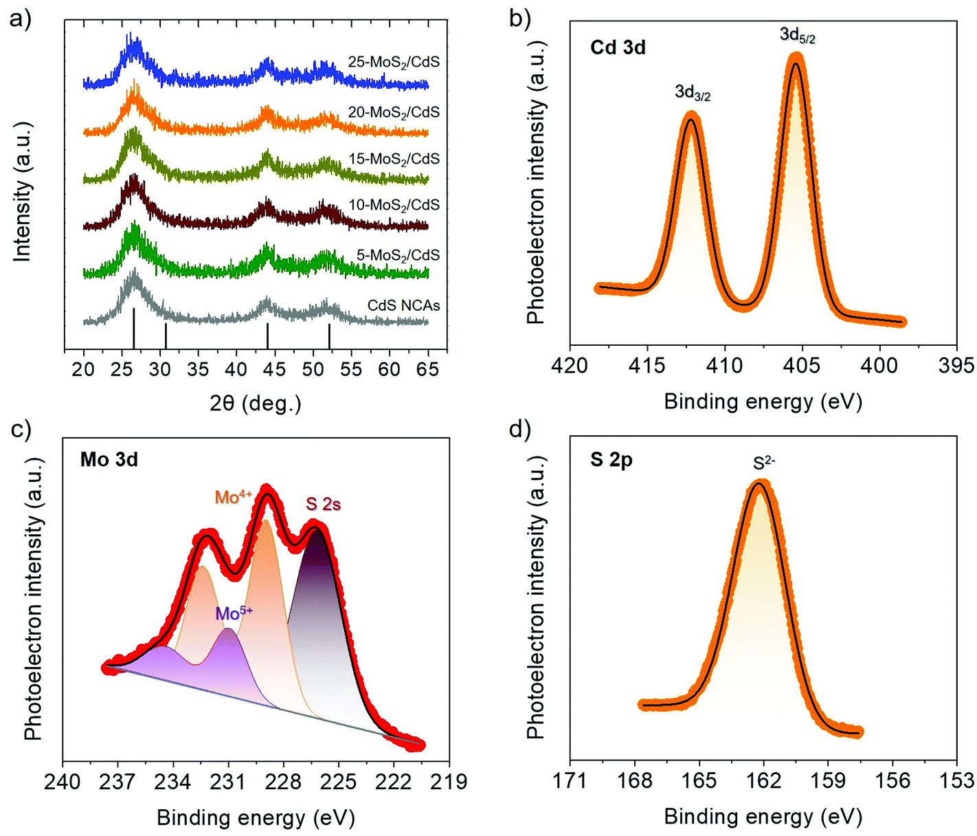 | ||
| Fig. 1 (a) XRD plots for the mesoporous CdS and MoS2/CdS NCAs. The standard diffraction data of the zinc blende CdS according to the JCPDS card no. 42-1411 are also shown (black bars). (b–d) Typical XPS core-level spectra of the Cd 3d (b), Mo 3d (c) and S 2p (d) region for the 20-MoS2/CdS catalyst. | ||
Typical XPS spectra of the best catalyst (20-MoS2/CdS) are shown in Fig. 1b–d. The XPS Cd 3d spectrum, in Fig. 1b, presents a doublet peak at 405.3 and 412.2 ± 0.2 eV binding energies, corresponding to the Cd 3d5/2 and Cd 3d3/2 core level lines of Cd2+ in CdS, respectively.32 The XPS spectrum of the Mo 3d scan confirmed the presence of Mo4+ species in MoS2, showing two peaks at 229.1 ± 0.2 eV (3d5/2) and 232.4 ± 0.2 eV (3d3/2) binding energies with a spin-obit splitting of 3.3 eV (Fig. 1c), in line with other reports.33 Besides the prominent Mo4+ 3d signal, there exists a weak doublet peak at a relatively higher binding energy (231 ± 0.2 eV and 234.4 ± 0.2 eV), which can be assigned to unsaturated Mo4+ atoms and/or higher oxidation state of Mo5+ species due to mild surface oxidation after the synthesis process.34 As for the singlet peak observed at 226.6 ± 0.2 eV, this is associated with the S 2s signal of sulfides (S2−).35 Furthermore, the XPS S 2p spectrum (Fig. 1d) exhibited a prominent peak at 162.2 ± 0.3 eV that is characteristic of the S2− ions in metal sulfides.36 Quantitative analysis of the XPS spectra also indicated a Mo-to-Cd atomic ratio close to 20.4:79.6 that corresponds to a ∼22.1 wt% MoS2 content, which is comparable to the composition obtained by EDS.
The morphology of the title materials was recorded via transmission electron microscopy (TEM), and the representative TEM images for the 20-MoS2/CdS sample are shown in Fig. 2. The images reveal that the framework of 20-MoS2/CdS is composed of approximately 4–5 nm sized CdS interconnected nanoparticles (Fig. 2a). In addition, from the high-resolution TEM (HRTEM) observation in Fig. 2b, some layered particles with a lateral dimension of around 10–15 nm can be discerned on the surface of CdS. A careful inspection reveals a layer-to-layer distance of ∼6.5 Å that reasonably correlates to the (002) planes of MoS2 NSs. This suggests a small enlargement of the interlayer distance of MoS2 NSs with respect to the bulk MoS2 (6.2 Å), which is due primarily to the small lateral size of the MoS2 layers. A similar effect was previously observed for other MoS2 nanostructures.37 Taken together with XPS characterization of the surface structure, these results confirm that small-size MoS2 NSs are anchored on the surface of linked CdS nanoparticles and, importantly, with a close contact that is advantageous for interfacial charge transfer and separation.
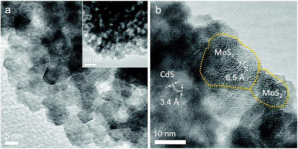 | ||
| Fig. 2 Representative (a) TEM and (b) HRTEM images of the 20-MoS2/CdS NCAs catalyst. | ||
The N2 physisorption method was applied to determine the porosity of the as-synthesized materials. The nitrogen adsorption and desorption isotherms and associated pore size distribution of the mesoporous 20-MoS2/CdS NCAs are compared as shown in Fig. 3a to those of unmodified CdS NCAs. The respective plots for the other MoS2-modified catalysts (i.e., with 5, 10, 15 and 25 wt% MoS2 content) are depicted in Fig. S3.† All samples display characteristic type-IV isotherms with a H2-type hysteresis loop (according to the International Union of Pure and Applied Chemistry classification), recommending mesoporous solids with interconnected pores.38 The resulting mesoporous MoS2/CdS architectures exhibit Brunauer–Emmett–Teller (BET) surface areas of 159–196 m2 g−1 and pore volumes of 0.20–0.26 cm3 g−1, which are slightly smaller than the values of the CdS pristine sample (225 m2 g−1 and 0.28 cm3 g−1, respectively). The pore width in these materials was estimated by applying the non-local density functional theory (NLDFT) fitting model on the adsorption data.39 The results reveal that all the samples have a quite narrow distribution of pore sizes with a peak maximum at ∼9.1 nm for CdS NCAs and ∼6.1–8.1 nm for the MoS2-modified catalysts (insets of Fig. 3a and S3†). The slight decrease in the porosity of composite materials with increasing MoS2 content can be attributed to the successful deposition of MoS2 NSs on the pore walls of mesoporous CdS, which is consistent with our TEM observations. The textural parameters for all the prepared materials are summarized in Table 1.
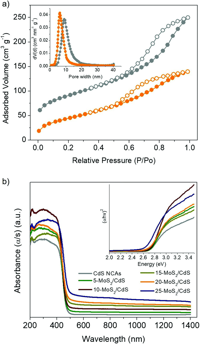 | ||
| Fig. 3 (a) N2 adsorption–desorption isotherms of the mesoporous CdS (gray symbols) and 20-MoS2/CdS (orange symbols) NCAs. The isotherm data of CdS NCAs are shifted by 30 cm3 g−1 for clarity. Inset: the NLDFT pore size distribution plots calculated from the adsorption data. (b) UV–vis/NIR diffuse reflectance spectra of mesoporous CdS and MoS2/CdS NCAs with 5, 10, 15, 20 and 25 wt% MoS2 content. Inset: the corresponding Tauc plots for direct bandgap semiconductors. | ||
To determine the optical absorption properties of CdS and MoS2/CdS NCAs, ultraviolet–visible/near-IR (UV–vis/NIR) diffuse reflectance spectroscopy was performed. As shown in Fig. 3b, the mesoporous CdS NCAs show an absorption edge of ∼457 nm (2.71 eV) due to the intrinsic electron transition from the valence band (VB) to the CB in CdS NCs. Note that, compared with typical bulk CdS (it has a bandgap of 2.4 eV), CdS NCAs exhibit a notable blue shift in the interband absorption, which probably results from the quantum confinement effect arising from the very small size of the constituent CdS NCs (ca. 4–5 nm in size according to TEM observations). Meanwhile, the absorption edge position of the MoS2-modified materials undergoes a small downshift upon increasing the concentration of MoS2. In particular, the bandgap energy (Eg) of the MoS2/CdS NCAs estimated according to the Tauc method [(αhv)2 ∝ (hv − Eg), where, α is the absorption coefficient and hv is the energy of incident photons] falls in the range of 2.63 to 2.71 eV, see the inset of Fig. 3b and Table 1. The tiny, yet noteworthy, small reduction of the energy bandgap is ascribed to the strong interactions between the CdS NCs and MoS2 layers, which allows electron transport across the interface to take place. Moreover, the MoS2-modified samples also showed a significant absorption tail in the 480–1400 nm range, which is most likely due to the visible and NIR light response of MoS2 NSs. Indeed, the intensity of this absorption progressively increases with increasing MoS2 content in composite samples and also correlates well with the absorption spectrum of MoS2 (Fig. S4†). The MoS2 NSs exhibit an energy gap of 1.62 eV that is greater than the typical bandgap of bulk MoS2 (∼1.3 eV), probably due to the small size and few-layered structure of the as-synthesized MoS2 nanolayers.
3.2 Photocatalytic evolution of H2
The photocatalytic H2 evolution activities of the different nanocatalysts were investigated under visible light irradiation (λ ≥ 420 nm), using an aqueous solution containing Na2S/Na2SO3 as the sacrificial reagent. Fig. 4a compares the rates of H2 production over the different MoS2-modified catalysts; the H2 evolution rates were determined during the first 2 h of illumination. It can be seen that bare CdS NCAs exhibit relatively poor H2 production performance (0.06 mmol h−1), which is primarily related to the fast recombination of photoexcited electron–hole pairs. On the contrary, MoS2 modification of catalysts led to a significant increase in photocatalytic activity, which is by a factor of 6.3× compared to CdS NCAs. In particular, the H2 evolution activity scales almost linearly with the MoS2 content and reaches a maximum (0.39 mmol h−1) at 20 wt%. The deposition of an excessive amount of MoS2 (25 wt%) apparently results in the light shading effect on CdS nanoparticles and/or the formation of interfacial charge-carrier recombination centers, leading to a decrease in the H2 production rate (0.29 mmol h−1). It should be noted that when MoS2 NSs were used as catalysts, no evolution of H2 was observed under the examined conditions (results not shown). Also, blank experiments in the absence of light or catalyst did not show any evolution of H2, indicating that H2 is produced by a photocatalytic reaction.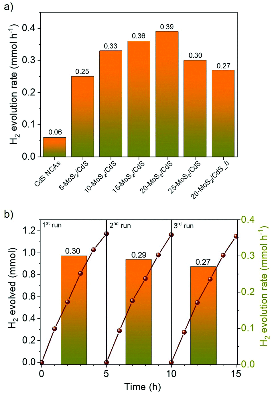 | ||
| Fig. 4 (a) H2 production rates for the mesoporous CdS and MoS2/CdS NCAs. The H2 evolution rate of the catalyst with 20 wt% bulk MoS2 (20-MoS2/CdS_b) is also given. (b) Photocatalytic recycling tests of the 20-MoS2/CdS NCAs. The columns show the H2 production rates of the 5 h time intervals. Reaction conditions: 20 mg catalyst (or 30 mg for recycling study), 20 mL aqueous solution of 0.35 M Na2S and 0.25 M Na2SO3, 300 W Xenon light source with a cut-off filter (λ ≥ 420 nm), 20 ± 2 °C. | ||
Besides chemical composition, morphological effects are an important aspect of the efficiency of the MoS2/CdS nanocatalysts. To elucidate this, we also prepared a reference catalyst by depositing 20 wt% of bulk MoS2 flakes (ca. 1.2–3 μm in lateral size)31 on the surface of mesoporous CdS NCAs (designated as 20-MoS2/CdS_b), and their H2 evolution performance was assessed under identical conditions (i.e., using 20 mg of the 20-MoS2/CdS_b catalyst dispersed in 0.35 M Na2S and 0.25 M Na2SO3 aqueous solution; λ ≥ 420 nm light radiation, 20 ± 2 °C). EDS analysis indicated that this catalyst contains 21.5 wt% MoS2 (Fig. S5a†). Also, it possesses almost identical textural and optical characteristics to those of the nanostructured 20-MoS2/CdS analogue, as inferred by XRD, N2 physisorption and UV–vis/NIR measurements, see Figs. S5b–d† and Table 1. Interestingly, the resultant 20-MoS2/CdS_b catalyst showed a 1.4× decrease of the H2 evolution performance (0.27 mmol h−1) over that of the 20-MoS2/CdS nanocatalyst (Fig. 4a), despite exhibiting very similar chemical composition, porosity and light absorption abilities. Therefore, the pronounced enhancement in the photocatalytic performance of 20-MoS2/CdS NCAs is clearly associated with the nanoscale interfacial contact between MoS2 nanolayers and CdS NCs, which probably contributes to an increased concentration of exposed S-edge sites of MoS2 and better electronic communication within the heterostructure. In general, reduction of the MoS2 layer size could increase the number of bridging S22− and terminal S2− edge atoms, which are the catalytic active sites in MoS2.40 As for the facile electron transfer from CdS to MoS2, this is further supported by photoluminescence and electrochemical studies (see below).
To optimize the reaction parameters, various photocatalytic H2 evolution tests were carried out using different sacrificial hole scavengers and mass loadings of the 20-MoS2/CdS catalyst. To this end, a series of sacrificial reagents, namely phenol, methanol, triethanolamine, triethylamine, lactic acid and Na2S/Na2SO3, were examined in 20 mL of water that contained a fixed amount of catalyst. As shown in Fig. S6,† we obtained optimal results with the S2−/SO3− mixture and used this sacrificial reagent during further studies. In general, S2− and SO3− ions not only enable H2 production by consuming the surface-reaching holes, but also S2− can replenish sulfur defects in metal sulfide materials originating from anodic photocorrosion.41 Also, photocatalytic tests using different concentrations of the 20-MoS2/CdS catalyst indicated that the rate of H2 evolution increases with increasing catalyst dose up to 1 g L−1 (Fig. S7†). We interpret this as the saturation in light absorption by the catalyst particles. For higher catalyst concentrations (1.5 g L−1), the slight reduction in the H2 production rate (0.30 mmol h−1) can be attributed to the light scattering effect of the catalyst particles. Overall, under the optimum reaction conditions (1 g L−1 catalyst dose; Na2S/Na2SO3 aqueous solution), 20-MoS2/CdS NCAs catalyze water splitting with a H2 production rate of ∼0.4 mmol h−1 (or ∼19 mmol h−1 g−1 mass activity) and a calculated apparent quantum yield (AQY) of 51.2% at 420 ± 10 nm. To the best of our knowledge, this efficiency far exceeds that of other MoS2-modified CdS photocatalysts in previous reports. A comparison of the H2 evolution activities of various MoS2-modified CdS photocatalysts is presented in Table S1.†
Except for high photocatalytic activity, the mesoporous 20-MoS2/CdS NCAs also exhibited persistent stability under the studied conditions. The stability of the catalyst was evaluated by repeated catalytic measurements for three cycles. Between each run, the catalyst was collected by centrifugation and re-suspended in a fresh Na2S/Na2SO3 solution. Also, before each catalytic test, the reaction mixture was bubbled with Ar gas for at least 30 min, so that no H2 and O2 gases were detected by gas-chromatography (GC). As shown in Fig. 4b, 20-MoS2/CdS presents a quite stable H2 evolution rate, retaining approximately 90% of its initial activity after three runs. Nevertheless, a small decline of the H2 production rate during the third run may be caused by minor photocorrosion and/or mass loss of catalyst during the recycling tests. EDS and N2 physisorption measurements were performed to verify the stability of the reused catalyst. The EDS spectra indicated a Mo/Cd atomic ratio of 19.9:80.1 that corresponds to a MoS2 content of about 21.6 wt%, while N2 physisorption data showed a surface area of 156 m2 g−1, pore size ∼6 nm and pore volume of 0.16 cm3 g−1 (Fig. S8†), very close to the values obtained from the fresh catalyst. Moreover, no change in the chemical state of elements in 20-MoS2/CdS NCAs was observed after the stability test, as shown by XPS spectra (see Fig. S9†), substantiating the excellent stability of the catalyst during the photocatalytic reactions.
3.3 Role of MoS2 NSs in the photochemical activity
To rationalize the role of MoS2 NSs on the catalytic performance and to better understand the charge-transfer dynamics at the nanoscale MoS2/CdS interfaces, we used electrochemical impedance spectroscopy (EIS). Fig. 5a depicts Mott–Schottky plots (1/CSC2versus applied voltage E curves) of the mesoporous CdS and MoS2/CdS NCAs; all the examined materials were drop-cast as thin films on a fluorinated tin oxide (FTO) glass substrate. From these plots, the flat band potentials (EFB) of the samples were determined using the tangent lines of the 1/Csc2 − E curves. As shown in Table 2, the obtained EFB values of MoS2/CdS NCA catalysts range from −0.68 V to −0.75 V, whereas the EFB position of CdS NCAs locates at −0.84 V; all electrochemical potentials are reported versus the reversible hydrogen electrode (RHE) at pH 7. Moreover, the positive slopes of the 1/Csc2 − E plots express that electrons are the majority charge-carriers (n-type conductivity) in these materials. By combining the EFB potentials with the respective bandgaps (as obtained from optical UV-vis/NIR spectroscopy), we obtained the band-edge potentials for each catalyst and the respective band-edge diagrams are presented in Fig. 5b. More specifically, for the calculation of band diagrams we have considered that the EFB level is located very close to the CB minimum of heavily doped n-type semiconductors and thus the VB potential (EVB) was obtained by adding the energy gap (Eg) to the EFB level; the calculated EVB values for each catalyst are listed in Table 2. As seen from the band diagrams, the EFB level progressively undergoes an anodic shift from −0.84 V to −0.68 V with increasing the MoS2 NS content on the surface of CdS. Moreover, as deduced from the magnitude of the slopes of 1/CSC2vs. E plots, MoS2 modification also increases the donor density (ND) of the catalysts. The measured ND values for the MoS2/CdS NCAs range from 1.17 to 1.70 × 1017 cm−3, which are significantly larger than that obtained for the unmodified CdS NCAs (5.87 × 1016 cm−3), as shown in Table 2. The observed anodic shift at the EFB position of MoS2/CdS NCAs can be interpreted by the lower EFB of MoS2 NSs (i.e., −0.68 V vs. RHE, as determined through Mott–Schottky measurements, see Fig. S10a†) compared to that of CdS mesoporous. This results in the formation of an internal electric field across the MoS2/CdS junction (upon contact) that drives electrons from CdS to MoS2 until the Fermi levels reach equilibrium; for heavily n-doped semiconductors (such as CdS NCs and MoS2 NSs), we assume that the Fermi level is located near to the CB edge position. Such an electron flow forms a depletion layer at the CdS surface, which lowers the CB energy potential closer to that of MoS2. Indeed, the intrinsic electric field at the contact interface can result in an increase in charge separation and, therefore, in electron donor density (ND) at the MoS2/CdS junctions, which is in line with the above Mott–Schottky analysis results.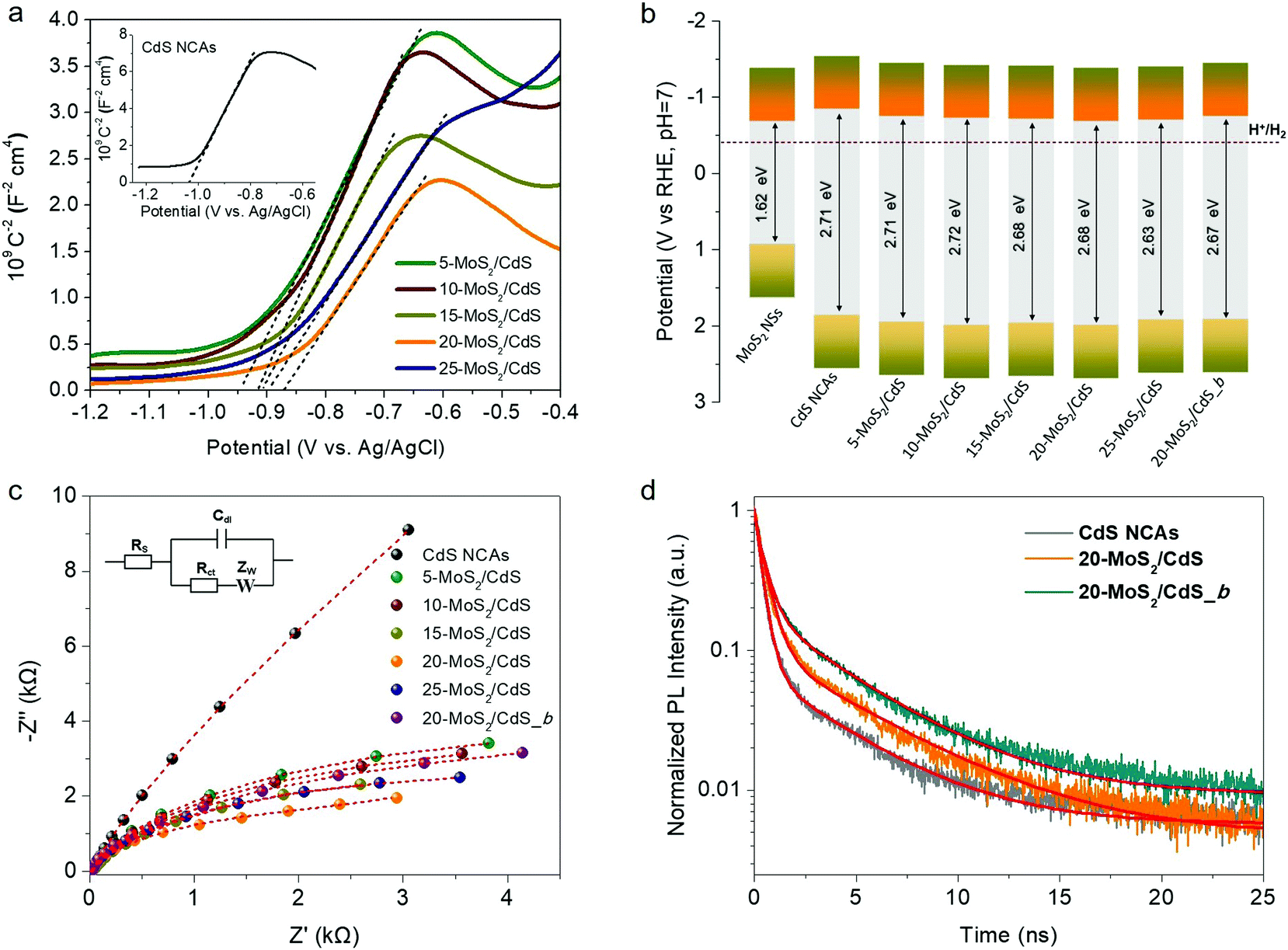 | ||
| Fig. 5 (a) Mott–Schottky plots of the MoS2-modified CdS NCAs (inset: the Mott–Schottky plot of CdS NCAs). (b) Band-edge positions and (c) Nyquist plots for MoS2 NSs, CdS NCAs and various MoS2-modified CdS NCAs (inset: equivalent circuit model Rs[Cdl/(Rct + Zw]). (d) Comparative time-resolved photoluminescence (TRPL) decay profiles of pristine CdS and MoS2-modified CdS NCAs with 20 wt% MoS2 NSs (20-MoS2/CdS) and MoS2 bulk flakes (20-MoS2/CdS_b). | ||
| Catalyst | E FB | E VB | Donor density (ND, cm−3) | R ct (kΩ) |
|---|---|---|---|---|
| (V vs. RHE, pH 7) | ||||
| MoS2 NSs | −0.68 | 0.94 | 6.89 × 10¹⁷ | |
| CdS NCAs | −0.84 | 1.87 | 5.87 × 10¹⁶ | 13.5 |
| 5-MoS2/CdS | −0.75 | 1.96 | 1.17 × 10¹⁷ | 6.3 |
| 10-MoS2/CdS | −0.72 | 2.00 | 1.22 × 10¹⁷ | 5.6 |
| 15-MoS2/CdS | −0.71 | 1.97 | 1.43 × 10¹⁷ | 5.3 |
| 20-MoS2/CdS | −0.68 | 2.00 | 1.70 × 10¹⁷ | 2.7 |
| 25-MoS2/CdS | −0.69 | 1.94 | 1.65 × 10¹⁷ | 4.5 |
| 20-MoS2/CdS_b | −0.75 | 1.92 | 1.13 × 10¹⁷ | 5.2 |
Moreover, the charge transfer properties of the prepared catalysts were also studied by EIS Nyquist plots. Fig. 5c shows the Nyquist plots of pristine and MoS2-modified CdS samples recorded in the 0.5 M Na2SO4 electrolyte under open circuit conditions over a frequency span from 1 Hz to 1 MHz. A typical Randles equivalent circuit was used to fit the experimental data consisting of a solution resistance (Rs), a charge-transfer resistance (Rct), a double layer capacitance (Cdl) and a diffusional resistance element (Zw) (see the inset of Fig. 5c), and the results of the fitting parameters are given in Table S2.† Fitting results indicated that the MoS2-modified catalysts have Rct values of ∼2.7–6.3 kΩ, which are significantly lower than that of CdS NCAs (∼13.5 kΩ) (Table 2), suggesting a more favorable charge transfer across the MoS2/CdS junctions. Subsequently, this process contributes to the improved photocatalytic efficiency of the MoS2-modified catalysts. It is worth mentioning that among diverse MoS2/CdS catalysts, 20-MoS2/CdS NCAs possessed the lowest resistance in carrier mobility (∼2.7 kΩ), which associates well with their remarkable photocatalytic H2 evolution performance. Notably, the bulk reference catalyst (20-MoS2/CdS_b) manifests a relatively higher Rct value (∼5.2 kΩ) than the nanostructured analogue (20-MoS2/CdS), thereby suggesting more sluggish charge transfer kinetics, despite having similar composition and band edge positions (see Fig. 5b and Fig. S10b†). In addition, as shown in Table 2, the charge carrier density of 20-MoS2/CdS_b is lower than that of 20-MoS2/CdS according to the Mott–Schottky equation (1.13 × 10¹⁷vs. 1.70 × 1017 cm−1), suggesting an inferior electronic contact between the bulk MoS2 layers and CdS nanostructure. This observation agrees with Nyquist charge-transfer resistance measurements and confirms that the nanoscale dimensionality of the MoS2 layers has a prominent impact on the charge separation dynamics at the MoS2/CdS interfaces. This is also elaborated by the photoluminescence (PL) study of catalysts under 375 nm excitation wavelength. As shown in Fig. S11,† the 20-MoS2/CdS catalyst shows a weaker PL emission at ∼460 nm (corresponding to the near band-edge excitonic relaxation) than the pristine CdS and bulk 20-MoS2/CdS_b samples, indicating better mitigation of electron–hole recombination by the nanoscale MoS2/CdS junctions.
The dynamics of charge-carrier recombination in these materials was also investigated using time-resolved photoluminescence (TRPL) decay measurements upon monochromatic excitation at 375 nm. To extract the PL lifetimes, we used a biexponential function [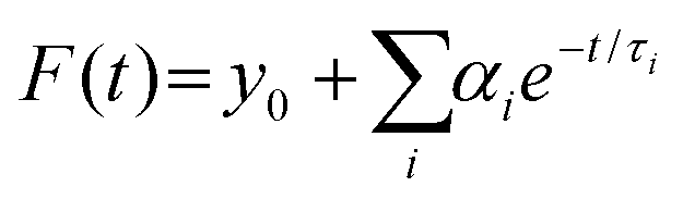 , i = 1, 2] to fit the PL decay data, where αi denotes the amplitude fractions
 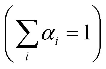 and τi is the carrier lifetime (Fig. 5d); we used a two-component equation describing the surface and possible defect-mediated (fast) and bulk (slow) radiative charge-carrier recombination, respectively. Through this fitting analysis the average lifetimes (τav) of mesoporous CdS, 20-MoS2/CdS and 20-MoS2/CdS_b catalysts were determined as 3.12, 4.15 and 3.46 ns, respectively; the fitting parameters of the PL decay curves are listed in Table S3.† Once again, TRPL results evidence that the formation of MoS2/CdS nanojunctions has a prominent impact on the charge-transfer kinetics at the catalyst interface, promoting a better separation of charge carriers and a more efficient utilization of the long-lived photoexcited electrons for the H2 evolution reaction, in line with the respective decrease of PL intensity shown in Fig. S11.† This is also apparent in the current density–voltage (J–V) data provided in Fig. S12,† which indicates a substantially lower proton reduction potential (by 0.18 V) in MoS2-modified catalysts compared to the pristine CdS. The observed positive shift in the onset potential with MoS2 deposition can be ascribed to the increased charge separation at the MoS2/CdS interface and the lower energy barrier for H2 evolution at the MoS2 edge sites. Moreover, in comparison to the bulk reference catalyst (20-MoS2/CdS_b), 20-MoS2/CdS NCAs exhibited a quick current response, implying more rapid reaction kinetics caused by the low dimensionality of MoS2 layers and increased amount of active MoS2 edge-sites. For example, the current density at an applied voltage of −1.1 V versus Ag/AgCl is greatly enhanced from 0.65 mA cm−2 to 1.34 mA cm−2 with 20-MoS2/CdS_b and 20-MoS2/CdS catalyst, respectively.
According to the above analysis, a possible reaction mechanism for the photocatalytic H2 evolution reaction by MoS2/CdS nanocatalysts was suggested, as presented in Scheme 1. Light irradiation first excites the electrons from the VB of CdS and MoS2 to their respective CB, producing photogenerated carriers. Subsequently, due to the lower CB potential of MoS2 than CdS and the intrinsic electric field formed at their contact interface, electrons are transferred from CdS to the active edge sites of MoS2 NSs, where they efficiently reduce H+ to H2. The smooth charge transfer and abated electron–hole recombination, which are effectively induced by the nanoscale MoS2/CdS junctions, would provide prolonged lifetime and thus more possibilities for electrons to engage in catalytic proton reduction. In parallel, the photoexcited holes on the surface of CdS and/or MoS2 oxidize the sacrificial reagents (such as S2− and SO32−). Evidence of such charge-transfer pathways within the MoS2/CdS nanojunction network was found from EIS and TRPL studies.
 | ||
| Scheme 1 Expected charge transfer during photocatalytic H2 production on mesoporous MoS2/CdS NCAs under visible light excitation. | ||
4. Conclusions
In summary, nanojunction networks of sub 5 nm sized CdS NCs and ultrasmall MoS2 NSs (ca. 10–15 nm in lateral size) with different compositions have been successfully synthesized by depositing MoS2 NSs on the surface of mesoporous CdS NC assemblies. The chemical composition, crystallinity and morphology of the prepared catalysts were confirmed by electron microprobe analysis, X-ray diffraction, electron microscopy, N2 porosimetry and X-ray photoelectron spectroscopy measurements. These mesoporous structures have a proper electronic structure that allows spatial separation and transport of charge carriers across the MoS2/CdS nano-interfaces and promotes high H2 production efficiency of the photoexcited electrons. Evidence for this was provided by photoluminescence and electrochemical impedance spectroscopy. Owing to these unique characteristics, the MoS2/CdS nanojunction network with the optimized MoS2 content (20 wt%) attains a 6.3× and 1.4× increase in the H2 production rate compared to bare mesoporous CdS and the bulk MoS2/CdS analogue, respectively. It also presents an energy conversion efficiency of 51.2% at 420 ± 10 nm, which is one of the highest reported for MoS2-modified CdS catalysts. The recycling test indicated persistent H2 evolution activity and excellent chemical and structural stability of the nanoparticle-assembled structure. The results of this study provide an understanding of the charge transfer dynamics at the MoS2/CdS nanoscale junctions and support the potential viability of the present MoS2-modified CdS nano-architectures as photocatalysts for clean energy conversion.Author contributions
Ch. Patriarchea: investigation, formal analysis, writing – original draft; I. Vamvasakis: investigation, formal analysis, writing – original draft; E. D. Koutsouroubi: investigation, formal analysis; G. S. Armatas: conceptualization, supervision, resources, writing – review and editing.Conflicts of interest
There are no conflicts to declare.Acknowledgements
This work was supported by the Hellenic Foundation for Research and Innovation H.F.R.I. (ELIDEK) under the “First Call for H.F.R.I. Research Projects to support Faculty Members & Researchers and the Procurement of High-cost research equipment grant” (project number: 400).Notes and references
- M. G. Walter, E. L. Warren, J. R. McKone, S. W. Boettcher, Q. Mi, E. A. Santori and N. S. Lewis, Solar water splitting cells, Chem. Rev., 2010, 110, 6446–6473 CrossRef CAS PubMed.
- D. G. Nocera, The artificial leaf, Acc. Chem. Res., 2012, 45, 767–776 CrossRef CAS PubMed.
- Y. Tachibana, L. Vayssieres and J. R. Durrant, Artificial photosynthesis for solar water-splitting, Nat. Photonics, 2012, 6, 511–518 CrossRef CAS.
- S. J. A. Moniz, S. A. Shevlin, D. J. Martin, Z.-X. Guo and J. Tang, Visible-light driven heterojunction photocatalysts for water splitting – a critical review, Energy Environ. Sci., 2015, 8, 731–759 RSC.
- Y. Liu, H. Wang, X. Yuan, Y. Wu, H. Wang, Y. Z. Tan and J. W. Chew, Roles of sulfur-edge sites, metal-edge sites, terrace sites, and defects in metal sulfides for photocatalysis, Chem. Catal., 2021, 1, 44–68 CrossRef.
- Y. Liu, P. D. Kanhere, C. L. Wong, Y. Tian, Y. Feng, F. Boey, T. Wu, H. Chen, T. J. White, Z. Chen and Q. Zhang, Hydrazine-hydrothermal method to synthesize three-dimensional chalcogenide framework for photocatalytic hydrogen generation, J. Solid State Chem., 2010, 183, 2644–2649 CrossRef CAS.
- A. Kudo and Y. Miseki, Heterogeneous photocatalyst materials for water splitting, Chem. Soc. Rev., 2009, 38, 253–278 RSC.
- S. Chen, T. Takata and K. Domen, Particulate photocatalysts for overall water splitting, Nat. Rev. Mater., 2017, 2, 17050 CrossRef CAS.
- X.-Q. Qiao, Z.-W. Zhang, Q.-H. Li, D. Hou, Q. Zhang, J. Zhang, D.-S. Li, P. Feng and X. Bu, In situ synthesis of n–n Bi2MoO6 & Bi2S3 heterojunctions for highly efficient photocatalytic removal of Cr(vi), J. Mater. Chem. A, 2018, 6, 22580–22589 RSC.
- Y.-J. Yuan, D. Chen, Z.-T. Yu and Z.-G. Zou, Cadmium sulfide-based nanomaterials for photocatalytic hydrogen production, J. Mater. Chem. A, 2018, 6, 11606–11630 RSC.
- L. Cheng, Q. Xiang, Y. Liao and H. Zhang, CdS-Based photocatalysts, Energy Environ. Sci., 2018, 11, 1362–1391 RSC.
- L. Nie and Q. Zhang, Recent progress in crystalline metal chalcogenides as efficient photocatalysts for organic pollutant degradation, Inorg. Chem. Front., 2017, 4, 1953–1962 RSC.
- M. Luo, W. Yao, C. Huang, Q. Wu and Q. Xu, Shape-controlled synthesis of Pd nanoparticles for effective photocatalytic hydrogen production, RSC Adv., 2015, 5, 40892–40898 RSC.
- I. Vamvasakis, B. Liu and G. S. Armatas, Size effects of platinum nanoparticles in the photocatalytic hydrogen production over 3D mesoporous networks of CdS and Pt nanojunctions, Adv. Funct. Mater., 2016, 26, 8062–8071 CrossRef CAS.
- K. Chang, M. Li, T. Wang, S. Ouyang, P. Li, L. Liu and J. Ye, Drastic layer-number-dependent activity enhancement in photocatalytic H2 evolution over nMoS2/CdS (n ≥ 1) under visible light, Adv. Energy Mater., 2015, 5, 1402279 CrossRef.
- I. Vamvasakis, I. T. Papadas, T. Tzanoudakis, C. Drivas, S. A. Choulis, S. Kennou and G. S. Armatas, Visible-light photocatalytic H2 production activity of β-Ni(OH)2-modified CdS mesoporous nanoheterojunction networks, ACS Catal., 2018, 8, 8726–8738 CrossRef CAS.
- R. Tong, K. W. Ng, X. Wang, S. Wang, X. Wang and H. Pan, Two-dimensional materials as novel co-catalysts for efficient solar-driven hydrogen production, J. Mater. Chem. A, 2020, 8, 23202–23230 RSC.
- A. K. Singh, P. Kumar, D. J. Late, A. Kumar, S. Patel and J. Singh, 2D layered transition metal dichalcogenides (MoS2): Synthesis, applications and theoretical aspects, Appl. Mater. Today, 2018, 13, 242–270 CrossRef.
- S. Manzeli, D. Ovchinnikov, D. Pasquier, O. V. Yazyev and A. Kis, 2D transition metal dichalcogenides, Nat. Rev. Mater., 2017, 2, 17033 CrossRef CAS.
- L. Wang, X. Liu, J. Luo, X. Duan, J. Crittenden, C. Liu, S. Zhang, Y. Pei, Y. Zeng and X. Duan, Self-optimization of the active site of molybdenum disulfide by an irreversible phase transition during photocatalytic hydrogen evolution, Angew. Chem., 2017, 129, 7718–7722 CrossRef.
- M. R. Saber, G. Khabiri, A. A. Maarouf, M. Ulbricht and A. S. G. Khalil, A comparative study on the photocatalytic degradation of organic dyes using hybridized 1 T/2H, 1 T/3R and 2H MoS2 nano-sheets, RSC Adv., 2018, 8, 26364–26370 RSC.
- A. B. Laursen, S. Kegnæs, S. Dahl and I. Chorkendorff, Molybdenum sulfides—efficient and viable materials for electro - and photoelectrocatalytic hydrogen evolution, Energy Environ. Sci., 2012, 5, 5577–5591 RSC.
- Z. Liang, R. Shen, Y. H. Ng, P. Zhang, Q. Xiang and X. Li, A review on 2D MoS2 cocatalysts in photocatalytic H2 production, J. Mater. Sci. Technol., 2020, 56, 89–121 CrossRef.
- Z.-W. Zhang, Q.-H. Li, X.-Q. Qiao, D. Hou and D.-S. Li, One-pot hydrothermal synthesis of willow branch-shaped MoS2/CdS heterojunctions for photocatalytic H2 production under visible light irradiation, Chin. J. Catal., 2019, 40, 371–379 CrossRef CAS.
- M. Xiong, J. Yan, B. Chai, G. Fan and G. Song, Liquid exfoliating CdS and MoS2 to construct 2D/2D MoS2/CdS heterojunctions with significantly boosted photocatalytic H2 evolution activity, J. Mater. Sci. Technol., 2020, 56, 179–188 CrossRef.
- S. R. Kadam, S. W. Gosavi, B. B. Kale, N. Suzuki, C. Terashima and A. Fujishima, Unique CdS@MoS2 core shell heterostructure for efficient hydrogen generation under natural sunlight, Sci. Rep., 2019, 9, 12036 CrossRef PubMed.
- I. Vamvasakis, K. S. Subrahmanyam, M. G. Kanatzidis and G. S. Armatas, Template-directed assembly of metal–chalcogenide nanocrystals into ordered mesoporous networks, ACS Nano, 2015, 9, 4419–4426 CrossRef CAS PubMed.
- I. T. Papadas, I. Vamvasakis, I. Tamiolakis and G. S. Armatas, Templated self-assembly of colloidal nanocrystals into three-dimensional mesoscopic structures: A perspective on synthesis and catalytic prospects, Chem. Mater., 2016, 28, 2886–2896 CrossRef CAS.
- I. Vamvasakis, A. Trapali, J. Miao, B. Liu and G. S. Armatas, Enhanced visible-light photocatalytic hydrogen production activity of three-dimensional mesoporous p-CuS/n-CdS nanocrystal assemblies, Inorg. Chem. Front., 2017, 4, 433–441 RSC.
- S. Pathan and A. Patel, Novel heterogeneous catalyst, supported undecamolybdophosphate: synthesis, physico-chemical characterization and solvent-free oxidation of styrene, Dalton Trans., 2011, 40, 348–355 RSC.
- E. D. Koutsouroubi, I. Vamvasakis, I. T. Papadas, C. Drivas, S. A. Choulis, S. Kennou and G. S. Armatas, Interface engineering of MoS2-modified graphitic carbon nitride nano-photocatalysts for an efficient hydrogen evolution reaction, ChemPlusChem, 2020, 85, 1379–1388 CrossRef CAS PubMed.
- J. Yuan, J. Wen, Q. Gao, S. Chen, J. Li, X. Li and Y. Fang, Amorphous Co3O4 modified CdS nanorods with enhanced visible-light photocatalytic H2-production activity, Dalton Trans., 2015, 44, 1680–1689 RSC.
- N. M. D. Brown, N. Cui and A. McKinley, An XPS study of the surface modification of natural MoS2 following treatment in an RF-oxygen plasma, Appl. Surf. Sci., 1998, 134, 11–21 CrossRef CAS.
- P. A. Spevack and N. S. McIntyre, A Raman and XPS investigation of supported molybdenum oxide thin films. 2. Reactions with hydrogen sulfide, J. Phys. Chem., 1993, 97, 11031–11036 CrossRef CAS.
- A. Syariati, S. Kumar, A. Zahid, A. Ali El Yumin, J. Ye and P. Rudolf, Photoemission spectroscopy study of structural defects in molybdenum disulfide (MoS2) grown by chemical vapor deposition (CVD), Chem. Commmun., 2019, 55, 10384–10387 RSC.
- D. Barreca, A. Gasparotto, C. Maragno and E. Tondello, Nanostructured cadmium sulfide thin films by XPS, Surf. Sci. Spectra, 2002, 9, 46–53 CrossRef CAS.
- Z. Chen, D. Cummins, B. N. Reinecke, E. Clark, M. K. Sunkara and T. F. Jaramillo, Core–shell MoO3−MoS2 nanowires for hydrogen evolution: A functional design for electrocatalytic materials, Nano Lett., 2011, 11, 4168–4175 CrossRef CAS PubMed.
- M. Thommes, Physical adsorption characterization of nanoporous materials, Chem. Ing. Tech., 2010, 82, 1059–1073 CrossRef CAS.
- P. I. Ravikovitch, D. Wei, W. T. Chueh, G. L. Haller and A. V. Neimark, Evaluation of pore structure parameters of MCM-41 catalyst supports and catalysts by means of nitrogen and argon adsorption, J. Phys. Chem. B, 1997, 101, 3671–3679 CrossRef CAS.
- L. R. L. Ting, Y. Deng, L. Ma, Y.-J. Zhang, A. A. Peterson and B. S. Yeo, Catalytic activities of sulfur atoms in amorphous molybdenum sulfide for the electrochemical hydrogen evolution reaction, ACS Catal., 2016, 6, 861–867 CrossRef CAS.
- N. Buehler, K. Meier and J. F. Reber, Photochemical hydrogen production with cadmium sulfide suspensions, J. Phys. Chem., 1984, 88, 3261–3268 CrossRef CAS.
Footnote |
| † Electronic supplementary information (ESI) available: Comparative catalytic data; XRD, UV-vis/NIR and EIS plots of MoS2 NSs; catalytic data and EIS, TRPL, EDS, XPS, PL, J-V and N2 physisorption plots of CdS and various MoS2-modified CdS NCAs. See DOI: 10.1039/d1qi01278a |
| This journal is © the Partner Organisations 2022 |