
 Open Access Article
 This Open Access Article is licensed under a
 Creative Commons Attribution 3.0 Unported Licence
Probing the energy levels of perovskite solar cells via Kelvin probe and UV ambient pressure photoemission spectroscopy†
J. R.
Harwell
a,
T. K.
Baikie
ab,
I. D.
Baikie
b,
J. L.
Payne
c,
C.
Ni
c,
J. T. S.
Irvine
c,
G. A.
Turnbull
*a and
I. D. W.
Samuel
*a
aOrganic Semiconductor Centre, SUPA, School of Physics and Astronomy, University of St Andrews, North Haugh, St Andrews, Fife KY16 9SS, UK. E-mail: gat@st-andrews.ac.uk; idws@st-andrews.ac.uk
bKP Technology Ltd, Burn Street, Wick, Caithness KW1 5EH, UK
cEaSTChem, School of Chemistry, St Andrews University, North Haugh, KY16 9SS, UK
First published on 7th July 2016
Abstract
The field of organo-lead halide perovskite solar cells has been rapidly growing since their discovery in 2009. State of the art devices are now achieving efficiencies comparable to much older technologies like silicon, while utilising simple manufacturing processes and starting materials. A key parameter to consider when optimising solar cell devices or when designing new materials is the position and effects of the energy levels in the materials. We present here a comprehensive study of the energy levels present in a common structure of perovskite solar cell using an advanced macroscopic Kelvin probe and UV air photoemission setup. By constructing a detailed map of the energy levels in the system we are able to predict the importance of each layer to the open circuit voltage of the solar cell, which we then back up through measurements of the surface photovoltage of the cell under white illumination. Our results demonstrate the effectiveness of air photoemission and Kelvin probe contact potential difference measurements as a method of identifying the factors contributing to the open circuit voltage in a solar cell, as well as being an excellent way of probing the physics of new materials.
Introduction
In the last 5 years, methylammonium lead halide perovskite solar cells have shown a rapid rise in performance to become one of the most promising new photovoltaic technologies. Methylammonium lead iodide (CH3NH3PbI3) and its variants exhibit strong absorption coefficients, high charge diffusion lengths, low exciton binding energies, and large ambipolar electron and hole mobilities.1–4 These favourable properties have allowed the efficiency of perovskite solar cells to increase from 4% in 20095 to more than 20% in 2015,6 showing that perovskites have the potential to play a major role in the next generation of photovoltaics. Since their emergence, much of the research on perovskite solar cells has focussed on the device architecture – using a wide range of hole and electron transporters in an attempt to achieve maximum efficiency.7–9 While this work has led to large improvements in power conversion efficiency, new approaches are required to better understand the device physics.The design of suitable device structures requires knowledge of the energy levels of each layer in the device. These must be favourable for electrons and holes to move to their respective contacts whilst minimising the energy lost due to carrier thermalisation. Both the highest occupied molecular orbital (HOMO) and Fermi levels (Ef) need to be considered, including how the latter is affected by the presence of other materials and light. This has been very important for the understanding of bulk heterojunctions in organic photovoltaics.10 Energy level alignment is also very important for perovskite solar cells, and so we report here a comprehensive study of the energy levels and Fermi levels of each component layer in a commonly used architecture of perovskite solar cell. We use UV ambient pressure photoemission spectroscopy (UV-APS) to accurately determine the HOMO of each material, and Kelvin probe to measure the surface Fermi level (or work function) in the dark and under white light illumination, i.e. surface photovoltage. Using this combination of techniques we gain an insight into how each layer affects the Fermi level of other layers as well as how their presence affects the white light response of the entire stack. The device architecture under study is a planar heterojunction TiO2/CH3NH3PbI3/2,2′,7,7′-tetrakis[N,N-di(4-methoxyphenyl)amino]-9,9′-spirobifluorene (spiro-OMeTAD) device using the lead acetate solution deposition method described by Zhang et al.11 The lead acetate route was chosen because it gives extremely reproducible films of high smoothness and quality whilst being processed in a nitrogen atmosphere with no need for humidity control, thus minimising variation between samples.
Experimental/theory
The instruments
Kelvin probe contact potential difference (CPD) measurements, as shown in Fig. 1(a), allow us to determine the Fermi level of a system to a resolution of 1–3 meV. This can provide useful insight into the properties of the material when combined with knowledge of the HOMO and LUMO, as the Fermi level is strongly affected by doping and the presence of other layers, while the HOMO and LUMO remain largely constant. In a doped semiconductor, the presence of p or n doping shifts the work function towards the HOMO or LUMO respectively. Thus measuring the Fermi level gives us a measure of the type and strength of doping in a material. The CPD technique can also be used to measure changes in the sample under illumination. This is valuable as it allows one to perform measurements on solar cell materials in what will be their standard operating state, as well as providing the ability to observe the surface photovoltage (SPV) due to the flattening of the bands12,13 in real time. This area of research is receiving increased interest, and some groups are already using Kelvin probe force microscopy – a separate but similar technique – to observe charge imbalance in perovskite solar cells under short circuit conditions.14 A preliminary study on the spectral response of the SPV of a perovskite solar cell has been performed.15 However the lead chloride deposition route used in that study gives rough and non-uniform films varying between 400 nm and 900 nm thickness. This results in a very small photovoltage by comparison to the expected voltage of a cell of this type.15 In our work we use a lead acetate deposition route, leading to smooth films and a surface photovoltage in line with the state-of-the-art devices of this structure, allowing us to make more direct links to real world operation.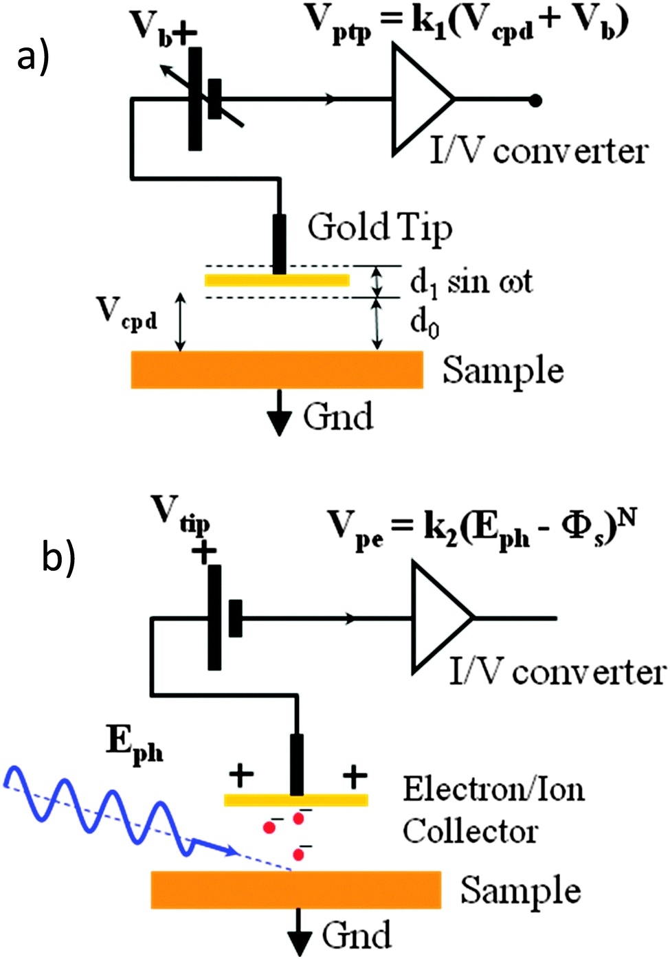 | ||
| Fig. 1 (a) Kelvin probe contact potential difference measurement: a vibrating gold tip (Kelvin probe) at potential Vb is suspended distance d0 above a grounded sample. The peak-to peak amplitude of the time-varying voltage from the tip Vptp is proportional to the sum of Vb and the contact potential difference Vcpd between the inner face of the vibrating tip and the sample surface. Off-null signal detection allows determination of Vcpd to within 1–3 meV. (b) UV – ambient pressure photoemission spectroscopy. The grounded sample is illuminated by a tuneable deep UV light source of photon energy Eph. Electrons are liberated at the sample surface, interact with air molecules16 to produce negative ions, which are collected by the positively biased tip (Vtip) a distance d0 away. The output voltage of the trans-impedance amplifier is proportional to (Eph − Φs)N, where N is 0.33 for semiconductors. | ||
UV-APS meanwhile exploits the photoelectric effect by measuring the number of photoelectrons that are emitted from a sample illuminated by tuneable monochromatic UV light. Photoelectrons are only emitted from the sample if the photon energy is greater than the depth of the HOMO, and so the HOMO can be determined by scanning the excitation photon energy and measuring the photocurrent. This measurement is usually carried out under ultra-high vacuum, as under ambient pressure the mean free path of the electrons (∼1 μm) is too short to reach the detector. However when measuring in ambient pressure, because the electrons are stopped very close to the surface of the sample, a cloud of charge builds up which creates O2−, OH− and N2− ions. These ions have a much larger mean free path than the electrons, so they can migrate to the sensor electrode to create a measurable current if a tip potential of +10 V is applied, thus allowing us to measure the emitted photocurrent indirectly. This method has previously been used by Baikie et al.16 to accurately measure the Fermi level of common metals, with close agreement to literature values.
A convenient feature of the apparatus is that the same sensor can be used for both Kelvin probe and UV-APS measurements. It is known that high energy UV light can damage a sample, particularly when it is in atmosphere as in this measurement. The applied intensity of UV light in this case is very low, but in order to be sure that there was no degradation of the sample, CPD measurements of the sample were taken before and after any APS measurement. In all cases in this report there was no change in Fermi level within margin of error, so it can be concluded that the sample is not degraded by the measurement.
Device fabrication
To fabricate the samples, pre-patterned Fluorine doped tin oxide (FTO) substrates were cleaned by sonicating in a solution of Helmanex detergent, acetone, and then isopropanol, before being dried and then plasma ashed for 3 minutes. To deposit the TiO2 layer, the samples were spin coated in air at 1500 RPM with a mildly acidic 1![[thin space (1/6-em)]](https://www.rsc.org/images/entities/char_2009.gif) :10 volume ratio solution of titanium isopropoxide and ethanol. The samples were then heated in stages to 100 °C, 150 °C, 325 °C, and 450 °C before finally being held at 500 °C for 30 min. The CH3NH3PbI3 precursor solution was made from methylammonium iodide and lead acetate at a 3:1 molar ratio dissolved in dimethyl formamide at a total concentration of 400 mg ml−1. A small amount (3 μl per ml) of hypophosphoric acid was added and the solution was spin coated at 2000 RPM for 45 s before being left at room temperature for 10 minutes then annealed at 100 °C for 5 minutes. The resultant perovskite layer was 150 nm thick. Spiro-OMeTAD was deposited from an 80 mg ml−1 solution in chlorobenzene containing additives of 11.6 μl per ml tert-butyl pyridine and 33.2 μl per ml of 0.61 M Li-TFSI solution in acetonitrile. Samples were then left in a desiccator overnight to oxygen dope before testing. To make solar cells, 80 nm silver contacts were deposited by evaporation at a rate of 0.1 nm s−1 under a vacuum of 10−6 mBar. All spin coating was done in a nitrogen filled glovebox. Once fabricated, all samples to be measured were stored in a desiccator until immediately prior to use.
:10 volume ratio solution of titanium isopropoxide and ethanol. The samples were then heated in stages to 100 °C, 150 °C, 325 °C, and 450 °C before finally being held at 500 °C for 30 min. The CH3NH3PbI3 precursor solution was made from methylammonium iodide and lead acetate at a 3:1 molar ratio dissolved in dimethyl formamide at a total concentration of 400 mg ml−1. A small amount (3 μl per ml) of hypophosphoric acid was added and the solution was spin coated at 2000 RPM for 45 s before being left at room temperature for 10 minutes then annealed at 100 °C for 5 minutes. The resultant perovskite layer was 150 nm thick. Spiro-OMeTAD was deposited from an 80 mg ml−1 solution in chlorobenzene containing additives of 11.6 μl per ml tert-butyl pyridine and 33.2 μl per ml of 0.61 M Li-TFSI solution in acetonitrile. Samples were then left in a desiccator overnight to oxygen dope before testing. To make solar cells, 80 nm silver contacts were deposited by evaporation at a rate of 0.1 nm s−1 under a vacuum of 10−6 mBar. All spin coating was done in a nitrogen filled glovebox. Once fabricated, all samples to be measured were stored in a desiccator until immediately prior to use.
Device testing
Measurements were taken using the KP Technology APS03 instrument, comprising UV-APS, scanning Kelvin probe (SKP) and surface photovoltage (SPV) sub-systems. The 2 mm diameter tip had a gold-alloy coating, and in contact potential difference (CPD) mode vibrates at 70 Hz with an amplitude of approximately 0.2 mm at an average height of 1 mm from the sample surface. UV-APS measurements were recorded immediately afterwards at this position, with a stationary tip. For UV-APS the sample is illuminated with a 4–5 mm diameter light spot derived from a tuneable monochromated D2 lamp (4–7 eV). The raw photoemission data are corrected for detector offset; intensity normalised then processed by a cube root power law. In Fig. 2 the photocurrent data are filtered with a Savitzky–Golay filter17 in order to remove the noise in the baseline signal where there is no photoemission. A comparison of the filtered and unfiltered data is shown in Fig. S1 (ESI†). The energy resolution in CPD mode is 1–3 meV and 50–100 meV in UV-APS mode.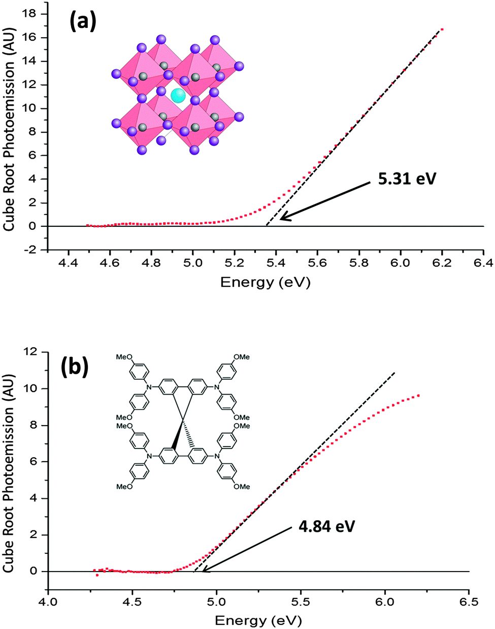 | ||
| Fig. 2 (a) Ambient pressure photoemission spectroscopy data for CH3NH3PbI3 on an FTO substrate. (b) Ambient pressure photoemission spectroscopy data for spiro-OMeTAD on an FTO substrate. The HOMO levels are determined by extrapolating the linear part of the curve down to the baseline signal level. The structures of the materials are shown in the inset of their respective graphs. | ||
For SPV measurements homogeneous illumination across the 10 × 10 mm2 sample was provided by a 150 W quartz halogen lamp coupled through a fibre optic and focussed onto the sample. The sample was mounted on a 3-axis motorised translation with 0.317 micron positioning resolution and the main enclosure provides both Faraday cage and light shield functions. Prior to mounting, the samples were held in a desiccator and conveyed to the APS-03 equipment using anti-static precautions. Dark CPD measurements were taken before absolute WF determination, which confirmed a stable Fermi level before and after exposure to monochromatic UV light, suggesting no surface charging or degradation. The UV-APS exposure time was approximately 100 s.
The exact routine of measurement for a given sample is as follows: samples are removed from the desiccator and a dark CPD measurement immediately performed, to be completed after 5 minutes of air exposure. The sample is then studied with air photoemission, and then with dark CPD again immediately after the UV exposure in order to confirm that there is no change in the sample over the course of the measurement. Surface photovoltage measurements are then performed before a final dark CPD measurement is taken to provide further confirmation that the sample is not changing. The total duration of air exposure is between 30 and 90 minutes for a full study. Measurements which showed a drift in work function over time were to be discarded. We are very confident that there was no degradation because any degradation of the samples would result in a drift in the sample work function over the course of the measurement, and because partial degradation would be visible in the air photoemission spectrum. Even though the samples spend relatively little time exposed to atmosphere, and no change is observed during the measurement, it is a concern for the CH3NH3PbI3 that a thin layer of PbI2 could quickly form on the surface on removal from the desiccator and affect the measurements. Since the APS probes up to 100 nm into the sample, a thin contaminant would not dominate the measurement and instead one would expect to see a second photoemission peak appear, corresponding to PbI2. No PbI2 peak is observed here, lending further evidence that the sample is not degraded in this way.
Results and discussion
A. HOMO and LUMO levels
Fig. 2(a) and (b) respectively show the photoemission spectra of CH3NH3PbI3 and spiro-OMeTAD (doped with bis(trifluoromethane) sulfonimide lithium (Li-TFSI) and tert-butylpyridine (TBP)) films on fluorine doped tin oxide (FTO) substrates. The photoemission is corrected to adjust for the lamp spectrum, and plotted on a cube root scale. It is empirically known that, in most semiconductors, the density of photoemission current increases with the cube root of the photon energy above the ionisation potential.18,19 Therefore a plot of the cube root of the photoemission against photon energy forms a straight line, which is extrapolated to the baseline signal to obtain the HOMO energy. In spiro-OMeTAD the threshold for photoemission is at a photon energy of 4.84 ± 0.05 eV, which corresponds to a HOMO at −4.84 ± 0.05 eV, while the CH3NH3PbI3 HOMO is at −5.31 ± 0.05 eV. The same results were obtained (within the experimental error) when a TiO2 layer was beneath them, providing the substrate was properly grounded. It is important to note that the photoemission from the underlying FTO and glass is several orders of magnitude weaker than that of CH3NH3PbI3 or spiro-OMeTAD, so we can be sure that the observed photoemission comes only from the intended material. No photoemission spectrum from TiO2 could be obtained, as its HOMO of −7.4 eV20 is deeper than our UV source was able to excite.CH3NH3PbI3 has been previously shown through ultra-high vacuum UV photoemission spectroscopy (UPS) to have a HOMO level between −5.4 eV21 and −5.3 eV,22 which closely matches our UV-APS value of −5.31 eV. This shows that the HOMO is not significantly affected by performing the measurement at ambient pressure. In addition, the UPS measurements are consistent between studies which fabricate the CH3NH3PbI3 under inert conditions and studies which fabricate in ambient conditions, showing that if there is a fast degradation process in air then it does not directly affect photoemission measurements.
To date, most literature measurements on the HOMO of spiro-Ometad come from cyclic voltammetry in solution, which reports values between −5.0 eV23 and −5.2 eV.24,25 Our value of −4.84 eV, measured in film, is significantly different and much more relevant to devices. It is well known that the ionisation potential can be different in solution from that in film due to polarisation effects.26 The significance of this result is that spiro-OMeTAD may not be as well matched to the perovskite HOMO of −5.31 eV as previously thought, meaning that there could be room for further optimisation.
B. CPD measurements
To investigate the layers using CPD, we first deposited single layers of spiro-OMeTAD, CH3NH3PbI3, and TiO2 onto separate FTO substrates in order to measure their Fermi levels in isolation from each other. CPD gives measurements relative to a gold reference sample of known Fermi level −4.87 eV (measured by UV-APS), rather than an absolute value. Hence the isolated CPDs of spiro-OMeTAD, CH3NH3PbI3, and TiO2 came to +100 mV, +229 mV, and −284 mV respectively, corresponding to Fermi levels of −4.97 eV, −5.10 eV, and −4.59 eV. For spiro-OMeTAD, the CPD results show that the Fermi level of spiro-OMeTAD lies almost exactly on top of the HOMO level, suggesting very strong p doping of the layer by the lithium salt. This concurs with literature reports from X ray photoelectron spectroscopy, that the presence of the Li-TFSI dopant in spiro-OMeTAD strongly shifts the Fermi level towards the HOMO,27 turning it into a hole transporter. It can also be seen that TiO2 is mildly n-doped as its Fermi level (−4.6 eV) is close to the known LUMO of −4.1 eV,20 while CH3NH3PbI3 appears to have p doping, as its Fermi level (−5.10 eV) deviates significantly from the bandgap centre of −4.65 eV. This is interesting as CH3NH3PbI3 made using lead chloride or lead iodide preparation routes tends to be n doped, with a work function of around 4.2 eV.28 This difference highlights how different processing techniques can give perovskite films with very different properties. The type of doping in CH3NH3PbI3 has previously been shown to be controlled by the dominant vacancy in the crystal – CH3NH3+ and Pb2+ vacancies lead to p doping while I− vacancies lead to n doping.29,30 Lead acetate as a precursor tends to create film morphologies with smaller crystal grains than other routes and also uses a 3:1 ratio of methylammonium iodide to lead acetate, so in this situation the lead is likely to be the ion in deficiency, which could result in Pb2+ vacancies and thus a perovskite that is more p doped than ones made by other routes. Additionally, the presence of the hypophosphorous acid additive has also been shown to help reduce the presence of metallic lead in the material, as well as to passivate trap states which normally form at the grain boundaries.31 This could also have an impact on the work function, so it is unsurprising that the observed Fermi level is different in this case.
C. Multilayer structures
The measurement was then applied to understand three multi-layered samples made of FTO/TiO2/CH3NH3PbI3, FTO/CH3NH3PbI3/spiro-OMeTAD, and FTO/TiO2/CH3NH3PbI3/spiro-OMeTAD. We found that the CPD of CH3NH3PbI3 changes from +229 mV (−5.10 eV) when on FTO alone, to −219 mV (−4.65 eV) when on TiO2. Since CPD measurements do not probe deeply into a sample's surface, the change must arise from charge flowing from the lower layer into the top layer, thereby changing the Fermi level. Similar but much less pronounced effects were observed when spiro-OMeTAD is deposited on CH3NH3PbI3, in that the Fermi level is “pulled” towards the Fermi level of the layer below. The Fermi level of the spiro-OMeTAD is increased by 55 meV as opposed to being decreased by more than 400 meV in the former case. A summary of the above results is shown in Table 1.| Material | HOMO level (eV) | LUMO level (eV) | Stable Fermi level (eV) |
|---|---|---|---|
| FTO (cleaned) | −4.9 | N/A | −4.9 |
| TiO2 (on FTO)20 | −7.4 | −4.1 | −4.6 |
| CH3NH3PbI3 (on FTO) | −5.3 | −3.7 | −5.1 |
| CH3NH3PbI3 (on TiO2) | −5.3 | −3.7 | −4.7 |
| Spiro-OMeTAD (on FTO) | −4.9 | −1.9 | −4.9 |
| Spiro-OMeTAD (on CH3NH3PbI3) | −4.9 | −1.9 | −4.9 |
These Fermi level “pulling” effects can be explained by band bending in the semiconductor layers. In semiconductors where the carrier concentration is low, the interface depletion region can extend across much of the thickness of the top material, causing the observed surface Fermi level to be shifted when compared to that of the material in isolation. In the case of CH3NH3PbI3 on TiO2, the depletion region in CH3NH3PbI3 has been previously measured by Kelvin probe force microscopy to be up to 300 nm thick.32 Given that the CH3NH3PbI3 layer in this experiment is only 150 nm thick, the depletion region is more than large enough to affect the surface work function of the CH3NH3PbI3, and the observed Fermi level is reduced and “pulled” towards the Fermi level of TiO2. The effect is similar, but less pronounced in spiro-OMeTAD because the carrier concentration in spiro-OMeTAD is higher, and its Fermi level is more closely matched to CH3NH3PbI3. In conjugated polymers a similar effect was observed by Tengstedt et al.33 who found that, due to a low carrier concentration, the observed Fermi level of the polymer was never deeper than that of its conducting substrate because the depletion region extends all the way through the organic layer. The materials in this study do not go to this extreme as their carrier concentration is higher than in most organics, however the depletion region is still large enough to alter the surface fermi level. It is worth noting that the TiO2 layer is very thin (20–40 nm) and as such is likely to be more affected by the underlying layer than the Spiro or CH3NH3PbI3 layers. This could explain why the observed work function (4.6 V) sits further below the LUMO (4.1 V) than one would expect for an n doped semiconductor. Perovskites have also been observed to have their Fermi levels strongly affected by the substrate they are deposited on, with n-type substrates shifting the Fermi energy towards the LUMO,28 which is consistent with our observations.
D. Surface photovoltage
After measuring the energy levels of the isolated materials and stacks of materials in the dark, we wanted to learn about the influence of light. We therefore illuminated our samples with white light in order to make surface photovoltage measurements. A stack of FTO/TiO2/CH3NH3PbI3/spiro-OMeTAD – essentially a complete solar cell minus the silver top contact – was fabricated, and its CPD was measured both in dark conditions and under illumination, as shown in Fig. 3(a). In the dark, the CPD was stable at +175 mV (−5.05 eV), but when the light was turned on the CPD dropped rapidly to −886 meV (−3.98 eV) – a change of more than 1050 meV. When the light was switched off, the Fermi level returned to its initial value with a slow decay (∼10 s) for the final part of the recovery which may be due to trapped or slow charges within the device. The process was repeated several times once the CPD had fully returned to its original value, and was shown to be very repeatable, with little change between cycles. The magnitude of the photovoltage shift, like the open circuit voltage of a solar cell, was strongly dependent on film quality, and as such it varied from sample to sample with a range of 750 mV to 1050 mV for the five sample batches studied.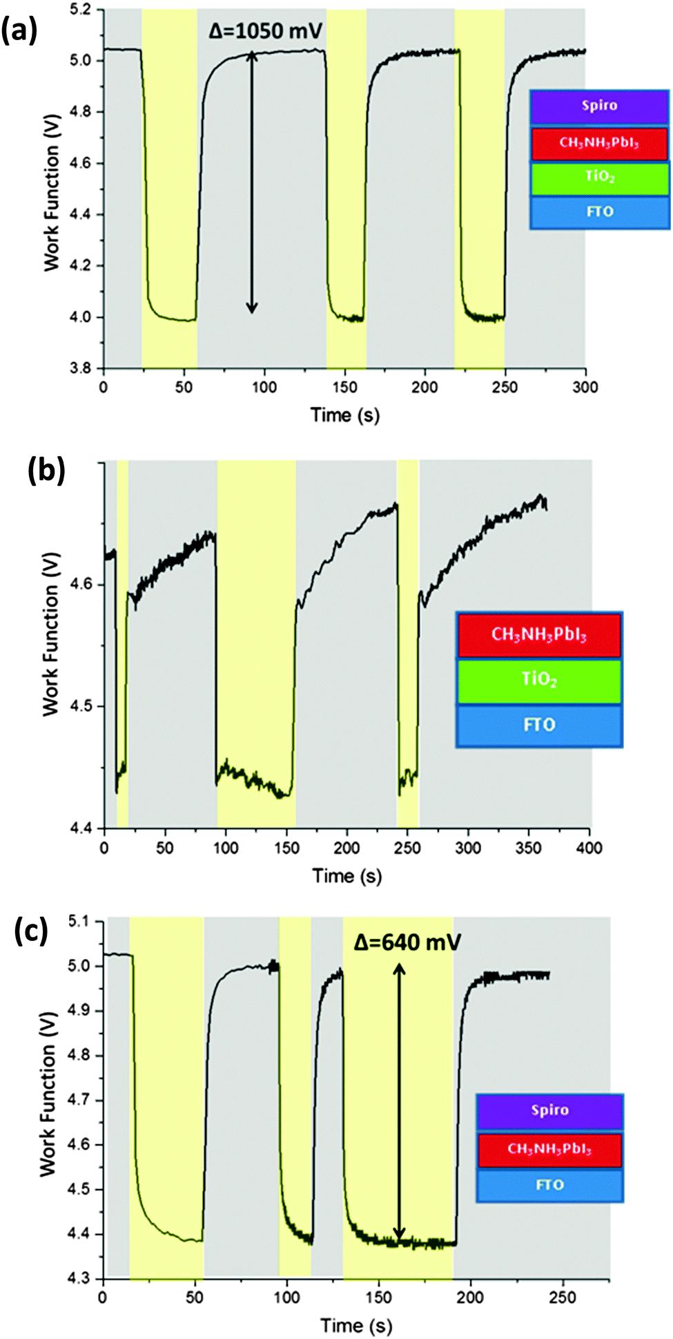 | ||
| Fig. 3 Light response of different stacks. In the yellow regions the light is on, while in the grey regions the light is off. (a) Shows the light response of a completed solar cell stack, (b) shows a stack with the spiro-OMeTAD layer omitted, and (c) shows a stack with the TiO2 omitted. The data is corrected from raw data to give absolute work function. | ||
In order to investigate the importance of each layer, different device architectures with layers removed were studied. The omission of either the TiO2 layer or the spiro-OMeTAD layer in the stack significantly reduced the magnitude of the photovoltage response, as can be seen in Fig. 3(b) and (c). For an FTO/TiO2/CH3NH3PbI3 stack (without spiro-OMeTAD), the Fermi level lowered by only about 200 meV under illumination, while in an FTO/CH3NH3PbI3/spiro-OMeTAD stack (missing TiO2) the shift was about 640 meV. It is worth noting that the CH3NH3PbI3 is much less stable when it is not covered with a spiro-OMeTAD capping layer, and so the CH3NH3PbI3 in the TiO2/CH3NH3PbI3 stack was observed to have a significant change in Fermi level with each light pulse. It is known that CH3NH3PbI3 is more vulnerable to degradation when under illumination,34 and this leads us to conclude that for this sample under illumination the observed Fermi level change was due to degradation to PbI2 in this sample, so it was not analysed further. We emphasise that there was no evidence of degradation in the other samples under this measurement, and that this degradation effect was only observed under illumination from high intensity light, and not during the dark CPD or air photoemission. As mentioned earlier, all other samples were stable for the duration of the measurement.
The measured surface photovoltage of the full stack of materials (1050 meV) is within the expected range for the open circuit voltage of a cell of this type (0.9 to 1.07 V). Fig. 4(a) shows a summary of all the HOMO, LUMO, and Fermi levels of all the materials in the stack when isolated from each other. Fig. 4(b) shows the equilibrium energies of the materials when electrically connected. Since the FTO layer is grounded, the Fermi level of all the materials are “pinned” to this energy causing the bands to bend at each interface. This results in a potential gradient for holes to move towards the spiro-OMeTAD, and for the electrons to move towards the TiO2. When the sample is illuminated, photogenerated electrons and holes move down the potential gradients and into the TiO2 and spiro-OMeTAD respectively, causing the Fermi levels to change, and a surface photovoltage to form. In the ideal situation dynamic equilibrium is reached when the build-up of charge has caused the bands to flatten completely, meaning no further charge builds up, and the surface photovoltage stabilises. The surface photovoltage represents the total Fermi level shift in the layers, and is equal in magnitude to the maximum open circuit voltage of the cell. Since the Fermi level of TiO2 is offset from the CH3NH3PbI3 by 450 mV, while the spiro-OMeTAD is offset by 650 mV, the bands will flatten completely once the TiO2 has shifted by 450 mV with respect to the CH3NH3PbI3, and the spiro-OMeTAD has shifted by 650 mV with respect to the CH3NH3PbI3. Thus the maximum Fermi level shift, and hence maximum open circuit voltage in the sample is 1100 meV. In the real sample, recombination losses prevent the surface photovoltage (SPV) reaching equilibrium at this point, and so the observed SPV of 1050 mV is slightly smaller than in the ideal situation. To our knowledge, the highest Voc observed in a solar cell of this design is 1070 mV,35 showing that if recombination is minimised then it is possible to get very close to the theoretical maximum of this model. It is also worth noting that, when we consider the FTO/CH3NH3PbI3/spiro-OMeTAD sample, the change in Fermi level under illumination is 640 meV. This is very close to the 650 meV change one would expect if one were to consider the band flattening between just the CH3NH3PbI3 and the spiro-OMeTAD, showing that our model is also able to explain the behaviour of the device structure with layers removed.
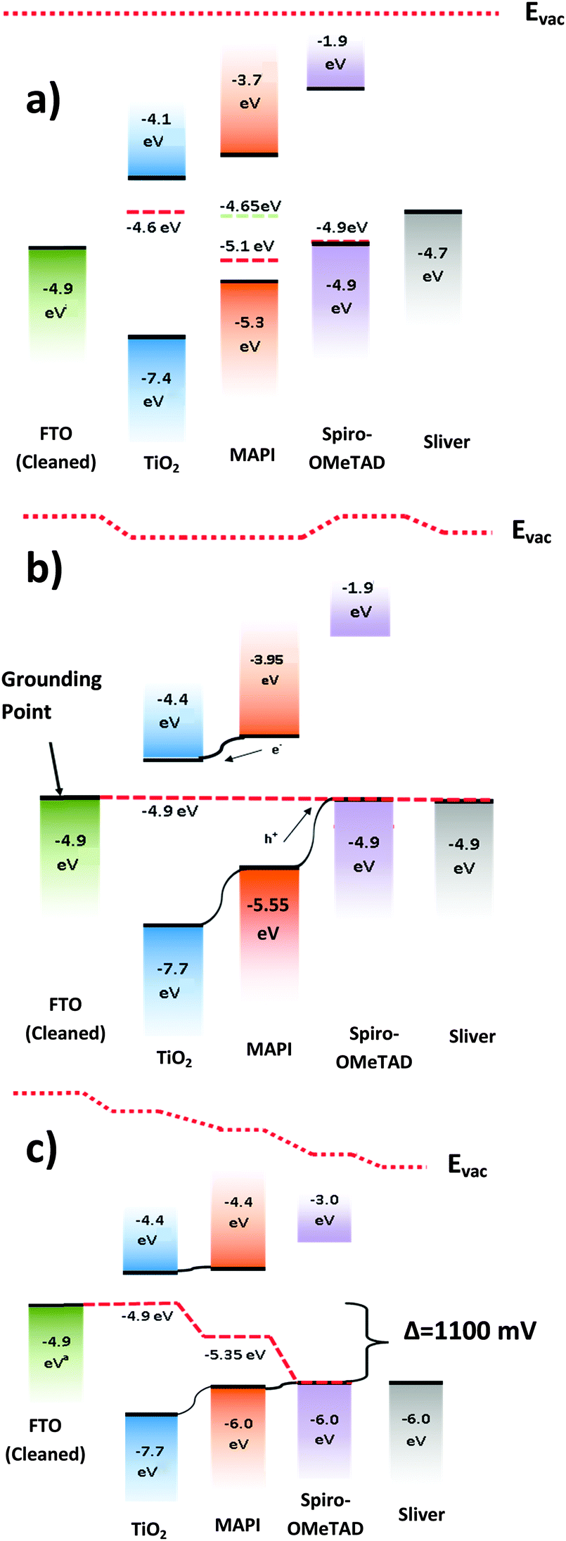 | ||
| Fig. 4 (a) A summary of the energy levels of the materials in isolation from each other. Red dashed lines show the Fermi levels measured in isolation, while the green dashed line shows the Fermi level for CH3NH3PbI3 (abbreviated to MAPI) when on a TiO2 substrate. (b) The solar cell at open circuit in dark conditions-the vacuum level has shifted for each layer so that the Fermi levels are aligned. There is a potential gradient for electrons to flow to the TiO2 and holes to the spiro-OMeTAD. (c) The cell under illumination – the vacuum levels shift until equilibrium is reached the band offset between the layers is flattened, removing the potential gradient for electrons and holes. The result is a Fermi level shift equal to the maximum open circuit voltage of the cell. | ||
Conclusions
In conclusion we have used a combination of ambient pressure photoemission and Kelvin probe contact potential difference measurements to get a detailed map of the energy levels of important and commonly used materials in perovskite solar cells. Using these data we are able to construct a band bending diagram of the workings of this cell, allowing us to make a prediction of the maximum open circuit voltage. We tested this prediction by studying the structure when under high intensity white light illumination, which allowed us to witness the band evolution of the solar cell in real time. By observing each layer both in isolation and as part of a stack, we are able to observe the effect of band bending on each material, as well as how critical each layer is to device performance. This insight, combined with the ability to quickly and reproducibly measure a wide variety of materials under ambient pressure, makes Kelvin probe and UV-APS powerful tools in the process of designing new solar cell materials and understanding the behaviour of multi-component stacks of optoelectronic materials.Acknowledgements
This work was supported by the Engineering and Physical Sciences Research Council (grant codes EP/M506631/1, EP/K015540/01, EP/K022237/1 and EP/M025330/1). IDWS and JTSI acknowledge Royal Society Wolfson research merit awards. The research data underpinning this manuscript can be found at http://dx.doi.org/10.17630/64e61735-c15f-4cd8-9edb-f950d21627b9.References
- S. D. Stranks, G. E. Eperon, G. Grancini, C. Menelaou, M. J. P. Alcocer, T. Leijtens, L. M. Herz, A. Petrozza and H. J. Snaith, Science, 2013, 342, 341–344 CrossRef CAS PubMed.
- V. D'Innocenzo, G. Grancini, M. J. P. Alcocer, A. R. S. Kandada, S. D. Stranks, M. M. Lee, G. Lanzani, H. J. Snaith and A. Petrozza, Nat. Commun., 2014, 5, 3586 Search PubMed.
- Q. Q. Lin, A. Armin, R. C. R. Nagiri, P. L. Burn and P. Meredith, Nat. Photonics, 2015, 9, 106–112 CrossRef CAS.
- X. Y. Chin, D. Cortecchia, J. Yin, A. Bruno and C. Soci, Nat. Commun., 2015, 6, 7383 CrossRef CAS PubMed.
- A. Kojima, K. Teshima, Y. Shirai and T. Miyasaka, J. Am. Chem. Soc., 2009, 131, 6050–6051 CrossRef CAS PubMed.
- W. S. Yang, J. H. Noh, N. J. Jeon, Y. C. Kim, S. Ryu, J. Seo and S. I. Seok, Science, 2015, 348, 1234–1237 CrossRef CAS PubMed.
- Y. L. Guo, C. Liu, K. Inoue, K. Harano, H. Tanaka and E. Nakamura, J. Mater. Chem. A, 2014, 2, 13827–13830 CAS.
- Q. Hu, J. Wu, C. Jiang, T. H. Liu, X. L. Que, R. Zhu and Q. H. Gong, ACS Nano, 2014, 8, 10161–10167 CrossRef CAS PubMed.
- Q. F. Xue, Z. C. Hu, J. Liu, J. H. Lin, C. Sun, Z. M. Chen, C. H. Duan, J. Wang, C. Liao, W. M. Lau, F. Huang, H. L. Yip and Y. Cao, J. Mater. Chem. A, 2014, 2, 19598–19603 CAS.
- K. Akaike, N. Koch, G. Heimel and M. Oehzelt, Adv. Mater. Interfaces, 2015, 2, 1500232 Search PubMed.
- W. Zhang, M. Saliba, D. T. Moore, S. K. Pathak, M. T. Horantner, T. Stergiopoulos, S. D. Stranks, G. E. Eperon, J. A. Alexander-Webber, A. Abate, A. Sadhanala, S. H. Yao, Y. L. Chen, R. H. Friend, L. A. Estroff, U. Wiesner and H. J. Snaith, Nat. Commun., 2015, 6, 6142 CrossRef CAS PubMed.
- K. Schwarzburg and F. Willig, J. Phys. Chem. B, 1999, 103, 5743–5746 CrossRef CAS.
- V. Ramamurphy and K. S. Schanze, Semiconductor Photochemistry And Photophysics, Marcel Dekker Inc., 2003, vol. 10 Search PubMed.
- V. W. Bergmann, S. A. L. Weber, F. J. Ramos, M. K. Nazeeruddin, M. Gratzel, D. Li, A. L. Domanski, I. Lieberwirth, S. Ahmad and R. Berger, Nat. Commun., 2014, 5, 5001 CrossRef CAS PubMed.
- L. Barnea-Nehoshtan, S. Kirmayer, E. Edri, G. Hodes and D. Cahen, J. Phys. Chem. Lett., 2014, 5, 2408–2413 CrossRef CAS PubMed.
- I. D. Baikie, A. Grain, J. Sutherland and J. Law, Phys. Status Solidi C, 2015, 12, 259–262 CrossRef CAS.
- A. Savitzky and M. J. E. Golay, Anal. Chem., 1964, 36, 1627–1639 CrossRef CAS.
- I. D. Baikie, A. C. Grain, J. Sutherland and J. Law, Energy Procedia, 2014, 60, 48–56 CrossRef CAS.
- I. D. Baikie, A. C. Grain, J. Sutherland and J. Law, Appl. Surf. Sci., 2014, 323, 45–53 CrossRef CAS.
- G. M. Liu, W. Jaegermann, J. J. He, V. Sundstrom and L. C. Sun, J. Phys. Chem. B, 2002, 106, 5814–5819 CrossRef CAS.
- P. Schulz, E. Edri, S. Kirmayer, G. Hodes, D. Cahen and A. Kahn, Energy Environ. Sci., 2014, 7, 1377–1381 CAS.
- P. Docampo, J. M. Ball, M. Darwich, G. E. Eperon and H. J. Snaith, Nat. Commun., 2013, 4, 2761 Search PubMed.
- T. Leijtens, I. K. Ding, T. Giovenzana, J. T. Bloking, M. D. McGehee and A. Sellinger, ACS Nano, 2012, 6, 1455–1462 CrossRef CAS PubMed.
- Y. K. Song, S. T. Lv, X. C. Liu, X. G. Li, S. R. Wang, H. Y. Wei, D. M. Li, Y. Xiao and Q. B. Meng, Chem. Commun., 2014, 50, 15239–15242 RSC.
- H. R. Li, K. W. Fu, A. Hagfeldt, M. Gratzel, S. G. Mhaisalkar and A. C. Grimsdale, Angew. Chem., Int. Ed., 2014, 53, 4085–4088 CrossRef CAS PubMed.
- J. L. Bredas, Mater. Horiz., 2014, 1, 17–19 RSC.
- R. Scholin, M. H. Karlsson, S. K. Eriksson, H. Siegbahn, E. M. J. Johansson and H. Rensmo, J. Phys. Chem. C, 2012, 116, 26300–26305 Search PubMed.
- E. M. Miller, Y. X. Zhao, C. C. Mercado, S. K. Saha, J. M. Luther, K. Zhu, V. Stevanovic, C. L. Perkins and J. van de Lagemaat, Phys. Chem. Chem. Phys., 2014, 16, 22122–22130 RSC.
- L. A. Frolova, N. N. Dremova and P. A. Troshin, Chem. Commun., 2015, 51, 14917–14920 RSC.
- Q. Wang, Y. C. Shao, H. P. Xie, L. Lyu, X. L. Liu, Y. L. Gao and J. S. Huang, Appl. Phys. Lett., 2014, 105, 163508 CrossRef.
- W. Zhang, S. Pathak, N. Sakai, T. Stergiopoulos, P. K. Nayak, N. K. Noel, A. A. Haghighirad, V. M. Burlakov, D. W. deQuilettes, A. Sadhanala, W. Z. Li, L. D. Wang, D. S. Ginger, R. H. Friend and H. J. Snaith, Nat. Commun., 2015, 6, 10030 CrossRef CAS PubMed.
- C. S. Jiang, M. J. Yang, Y. Y. Zhou, B. To, S. U. Nanayakkara, J. M. Luther, W. L. Zhou, J. J. Berry, J. van de Lagemaat, N. P. Padture, K. Zhu and M. M. Al-Jassim, Nat. Commun., 2015, 6, 8397 CrossRef CAS PubMed.
- C. Tengstedt, W. Osikowicz, W. R. Salaneck, I. D. Parker, C. H. Hsu and M. Fahlman, Appl. Phys. Lett., 2006, 88, 053502 CrossRef.
- Y. Han, S. Meyer, Y. Dkhissi, K. Weber, J. M. Pringle, U. Bach, L. Spiccia and Y. B. Cheng, J. Mater. Chem. A, 2015, 3, 8139–8147 CAS.
- M. Z. Liu, M. B. Johnston and H. J. Snaith, Nature, 2013, 501, 395–398 CrossRef CAS PubMed.
Footnote |
| † Electronic supplementary information (ESI) available. See DOI: 10.1039/c6cp02446g |
| This journal is © the Owner Societies 2016 |