DOI:
10.1039/D5TC00610D
(Paper)
J. Mater. Chem. C, 2025,
13, 11427-11437
Synthesis, characterization and OFET performance of A–D–A semiconducting small molecules functionalized with perylene diimide groups†
Received
12th February 2025
, Accepted 27th April 2025
First published on 12th May 2025
Abstract
Organic semiconductor molecules have been utilized in commercial applications owing to their outstanding advantages, such as tunable absorption spectra and electronic energy levels, and superior thermal stability. Three perylene diimide (PDI)-based small molecules have been synthesized and their chemical–physical, electrochemical and organic field effect transistor (OFET) properties have been characterized. Three different central IDT electron donor cores symmetrically functionalized with PDI electron-acceptor moieties and flanked in the terminal positions with alkyl groups were purposely designed. All the molecules consist of a PDI group as the acceptor (A) unit and indacenodithiophene (IDT) as the donor (D) unit. The impact of the acceptor–donor–acceptor (A–D–A) structures on the photoelectric performance of the molecules was investigated. The conjugated molecules exhibit full coverage absorption in the visible light spectrum, implying that they could be utilized for more potential applications in optoelectronic devices. All the molecules exhibited good thermal stability and typical n-type semiconductor behavior with a highest electron mobility of up to 2.09 × 10⁻¹ cm2 V−1 s−1 when Ion/Ioff = 104. S-PDI-IDT-2 exhibited ambipolar transport properties, with a hole transportation mobility on the order of 10−3.
1. Introduction
Organic semiconductors (OSCs) are key materials that have been applied in various organic electronic devices, such as OFETs and organic photovoltaics (OPVs)1–18 because of their low-cost, large-area fabrication, excellent mechanical flexibility and the ease with which their energy levels can be modulated through organic synthesis. In recent years, organic electronic products have received increasing attention in the fields of flexible displays and wearable devices. Among the many known electron acceptors, non-fullerene materials, such as PDI and its derivatives in particular have been researched extensively due to their low energy levels, high carrier mobility and other unique advantages associated with their charge carrier transport behaviors and photoelectric performance.5,8,10–17,19–43 However, the electron transfer pathways in PDI are restricted because of its self-aggregation behavior. Breaking this self-aggregation to achieve a twisted molecular geometry is an effective method to overcome this problem. Therefore, the molecular arrangement and stacking properties of PDI should be optimized by molecular design and investigation.44–46 IDT has been used as an electron-donating unit because IDT has a well-conjugated fused ring structure and branched hexylphenyl groups, which suppress the strong aggregation between the molecules, whilst the strong electron-donating ability of IDT leads to stronger intramolecular charge transfer (ICT).47–51
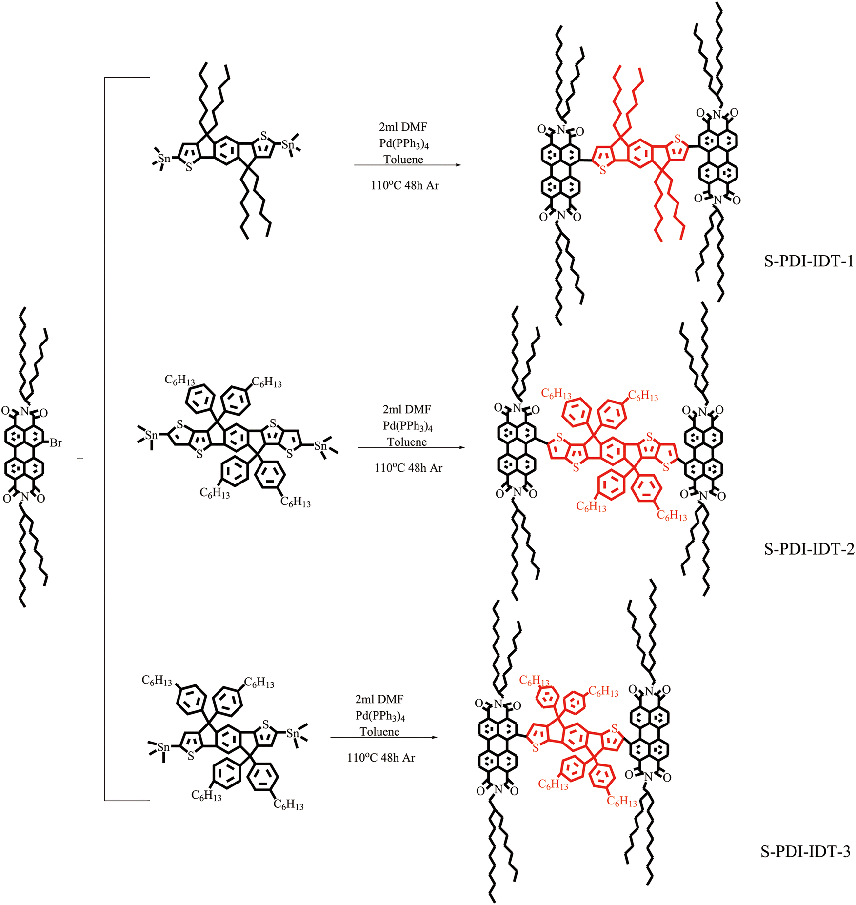
In this work, three molecules with branched alkyl chains were successfully synthesized via Stille coupling. The chemical structures are shown in Scheme 1. Three kinds of electron donor with IDT as the central core and symmetrically functionalized with PDI electron-acceptor moieties were purposely designed and a further extension of the molecular conjugation could be obtained via the use of cross coupling reactions in the preparation of the molecules. It was possible to obtain tailored tuning of the molecular orbitals energies and to achieve the optimization of the hole and electron mobilities of the OFETs by combining IDT units with PDI units. A–D–A structures were built and constructed as channels for efficient electron transport that allow electrons to be more delocalized, leading to a red shift and the extension of absorption bands.52 All the molecules were thoroughly characterized in terms of their thermal, structural, optical, and electrochemical properties. The molecules were finally processed as thin films and applied as active layers in OFETs to investigate their charge transport properties. The carrier mobility was tested in a glove box and all the examinations revealed that the three molecules exhibited n-type semiconductor transport capabilities. In the bottom gate/top contact (BGTC) OFET devices fabricated from the molecules, the molecules S-PDI-IDT-1, S-PDI-IDT-2 and S-PDI-IDT-3 demonstrated the highest charge mobilities of 4.59 × 10⁻² cm2 V−1 s−1, 4.59 × 10⁻² cm2 V−1 s−1 and 2.09 × 10⁻¹ cm2 V−1 s−1 in the glove box. GIWAXS and AFM were conducted to explore the microstructure of the thin films.
 |
| | Scheme 1 Synthesis of the three molecules. | |
2. Results and discussion
2.1. Synthesis and characterization
N,N′-Bis(2-octyldodecyl)-1-bromoperylene,3,4,9,10-tetracarboxylic diimide (PDI-Br), (4,4,9,9-tetrahexyl-4,9-dihydro-s-indaceno[1,2-b:5,6-b′]-dithiophene-2,7-diyl)bis(trimethylstannane) (IDT-1), 1,1′-[6,6,12,12-tetrakis(4-hexylphenyl)-6,12-dihydrodithieno[2,3-d:2′,3′-d′]-s-indaceno[1,2-b:5,6-b′]dithiophene-2,8-diyl]bis[1,1,1-trimethylstannane] (IDT-2), and (4,4,9,9-tetrakis(4-hexylphenyl)-4,9-dihydro-s-indaceno[1,2-b:5,6-b′]dithiophene-2,7-diyl)bis(trimethylstannane) (IDT-3) were obtained through direct purchase from Derthon Optoelectronic Materials Science Technology Co. Ltd, and were used without further purification. PDI-Br was reacted with IDT-1, IDT-2, and IDT-3via a Stille coupling reaction in nitrogen for 48 h in toluene solvent using 2 mL of dimethylformamide (DMF) and Pd(PPh3)4 (24 mg, 0.02 mmol). The molecules were dissolved in chloroform with minimum solvent and then methanol was added dropwise to the solution for precipitation. The crude products were further refined via column chromatography with a mixture of petroleum ether and dichloromethane (1![[thin space (1/6-em)]](https://www.rsc.org/images/entities/char_2009.gif) :1–1:1.5) as the eluent, yielding the target molecules S-PDI-IDT-1, S-PDI-IDT-2, and S-PDI-IDT-3. The structures of the molecules are displayed in Scheme 1 (for detailed 1H NMR data for each molecule see Fig. S4, S10, and S16 (ESI†). For detailed 13C NMR data for each molecule see Fig. S5, S11 and S17 (ESI†). For detailed high resolution mass spectrometry data for each molecule see Fig. S6, S12 and S18, ESI†).
:1–1:1.5) as the eluent, yielding the target molecules S-PDI-IDT-1, S-PDI-IDT-2, and S-PDI-IDT-3. The structures of the molecules are displayed in Scheme 1 (for detailed 1H NMR data for each molecule see Fig. S4, S10, and S16 (ESI†). For detailed 13C NMR data for each molecule see Fig. S5, S11 and S17 (ESI†). For detailed high resolution mass spectrometry data for each molecule see Fig. S6, S12 and S18, ESI†).
Thermogravimetric analysis (TGA) and differential scanning calorimetry (DSC) were carried out to characterize the thermal properties under a nitrogen atmosphere. Fig. 1(a) shows that all the molecules exhibit excellent thermal stability with decomposition temperatures (Td, 5% weight loss) of 459.82 °C, 472.31 °C, and 476.88 °C, which were all above 300 °C, thus demonstrating that the three molecules could be used for device preparation (for detailed data for each molecule see Fig. S2, S8 and S14, ESI†). The DSC curves in Fig. 1(b) of S-PDI-IDT-1 and S-PDI-IDT-3 show that there are no significant melting or crystallization transition peaks in the temperature range of 30–300 °C. An endothermic peak was observed in the DSC curve of S-PDI-IDT-2 at a temperature of 273 °C. For detailed data for each molecule see Fig. S3, S9 and S15 (ESI†). It is suggested that the molecules were nearly amorphous with no crystalline regions.
 |
| | Fig. 1 (a) TGA and (b) DSC analysis of the molecules measured at scan rate of 10 °C min−1 under an N2 atmosphere. | |
2.2. Optical and electrochemical properties and theoretical calculations
The UV-Vis-NIR absorption spectra of the molecules are shown in Fig. 2, and detailed data are shown in Table 1. The spectral absorption at 300–450 nm was attributed to the π–π* transition. The main absorption peaks that fall within the range of 300–450 nm for S-PDI-IDT-1, S-PDI-IDT-2, and S-PDI-IDT-3 were 389 nm, 428 nm and 389 nm in solution and 387 nm, 427 nm and 394 nm in the film state, respectively. A–D–A push–pull interactions between the A unit and D unit of the molecules contribute to a broad absorption in the range of 600–900 nm (for detailed data for each molecule see Fig. S1, S7 and S13, ESI†). The maximum absorption peaks (λmax) in the low-energy region were 684, 686, and 657 nm in solution and 704, 724, and 689 nm in the film state for S-PDI-IDT-1, S-PDI-IDT-2, and S-PDI-IDT-3, respectively. The film state exhibited a red-shift within the range of 20–30 nm. The absorption observed at these high wavelengths was attributed to the unique molecular architecture of the molecules as characterized by their tailored A–D–A groups. In another published manuscript53 in which the same monomers were polymerized and examined as n-type OFET semiconductors, the λmax of the polymer in the published manuscript was redshifted compared with the molecules due to the conjugation length of the polymer increasing. The absorption wavelengths exhibited by the molecules were distinctly modulated by the conjugated structure of the A–D–A groups. Therefore, an enhancement in the donor cores of IDT results in a shift of the absorption spectrum towards a higher λmax value. Observation of the structure of the three molecules shows that the conjugated plane of the IDT in S-PDI-IDT-1 is relatively small when compared to the other two molecules, and its possesses a higher λonset value in the absorption spectrum, which may be related to the regularity of its spatial molecular conformation.
 |
| | Fig. 2 Normalized UV-Vis-NIR absorption spectra of the molecules in chloroform (a) and in thin-film states spin-cast from chloroform solutions on quartz substrates (b). | |
Table 1 Molecular parameters and electrochemical properties
| Molecules |
λ
max
[nm] |
λ
onset [nm] |
E
optgb [eV] |
λ
max
[nm] |
| Solution |
Film |
Solution |
Film |
|
The maximum absorption peaks in the low-energy region.
E
optg = 1240/λonset (in the film).
The maximum absorption peaks in the range 300–450 nm.
|
|
S-PDI-IDT-1
|
684 |
704 |
853 |
1.45 |
389 |
387 |
|
S-PDI-IDT-2
|
686 |
724 |
822 |
1.51 |
428 |
427 |
|
S-PDI-IDT-3
|
657 |
689 |
826 |
1.50 |
389 |
394 |
The conjugated molecules exhibit absorption profiles that cover the full visible light spectrum. However, the optimal conformation of IDT-PDI was also highly twisted, and the dihedral angle between the IDT and PDI planes was ca. 50°, which results in molecular absorptions of less than 1000 nm.51 The information on the geometry, electronic structure, molecular conformation and molecular orbitals (HOMO and LUMO) of the three molecules was analyzed using density-functional theory with the B3LYP hybrid function and 6-311G(d,p) basis set. Gaussian 16 was applied to perform the theoretical molecular computations. Fig. 3 firmly confirms that the calculated dihedral angles between the IDT and PDI planes are 51.17°, 52.71° and 51.44°.
 |
| | Fig. 3 Optimal conformations of S-PDI-IDT-1 (a), S-PDI-IDT-2 (b), and S-PDI-IDT-3 (c), in which the alkyl groups are simplified to methyl groups. | |
From the calculated images (see Fig. 4) of the HOMO and LUMO of the molecules, it was seen that the HOMO energy levels were distributed on the central aromatic ring because the central IDT core remains electron-rich. The theoretical band gaps were 1.81 eV, 1.66 eV, and 1.79 eV for S-PDI-IDT-1, S-PDI-IDT-2, and S-PDI-IDT-3, respectively, which was slightly higher than the optical bandgap. Fig. 4 shows that the theoretically calculated HOMO levels were found to be −5.29 eV, −5.11 eV and −5.25 eV and the LUMO levels were found to be −3.48 eV, −3.45 eV and −3.46 eV for S-PDI-IDT-1, S-PDI-IDT-2, and S-PDI-IDT-3, respectively. From the perspective of the molecular structure, S-PDI-IDT-2 and S-PDI-IDT-3 had more side chains with benzene rings on the middle IDT plane compared to S-PDI-IDT-1, resulting in an increase in the steric hindrance of the molecules. Furthermore, the length of the middle IDT planes for S-PDI-IDT-3 was significantly smaller than that of S-PDI-IDT-2, resulting in a larger steric hindrance of the endcap PDI group. Thus, the distribution of the LUMO energy levels in the molecule was uneven, with a preferential distribution towards one side of the PDI. It also can be seen that the calculated LUMO for S-PDI-IDT-2 has its electron density localized less symmetrically than S-PDI-IDT-1. This is the reason that the steric hindrance of the molecule plays a vital role in its behavior.
 |
| | Fig. 4 Theoretically calculated HOMO and LUMO electron density distributions of (a) S-PDI-IDT-1, (b) S-PDI-IDT-2 and (c) S-PDI-IDT-3. | |
The energy levels were determined via cyclic voltammetry (CV) measurements in deoxygenated dichloromethane. The CV plots and the energy levels are shown in Fig. 5. The optical band gaps (Eoptg, eV) of the three molecules were calculated from the boundary absorption values using the formula given in Table 1. The calculated Eoptg values of the molecules were 1.45 eV for S-PDI-IDT-1, 1.51 eV for S-PDI-IDT-2, and 1.50 eV for S-PDI-IDT-3. Generally, greater conjugation and more rigid planes are beneficial for building electron transport channels. However, a comparison of S-PDI-IDT-2 with S-PDI-IDT-3 shows that the λonset values were almost the same, which indicates that the highly twisted conformation dominated the molecular absorption. The values of the HOMO and LUMO energy levels are summarized in Table 2. According to the CV plots in Fig. 5a, S-PDI-IDT-1, S-PDI-IDT-2, and S-PDI-IDT-3 displayed onset reduction potentials (Eonsetred) of −0.83 eV, −0.72 eV, and −0.74 eV, respectively. The LUMO energy levels of all the molecules were −3.57 eV, −3.68 eV and −3.57 eV for S-PDI-IDT-1, S-PDI-IDT-2 and S-PDI-IDT-3, respectively. All values were probably around −3.6 eV. Unfortunately, no peaks were observed in the oxidation scans of the molecules, except for the case of S-PDI-IDT-3. The HOMO energy values were extracted from the optical bandgap. The calculated HOMO energy levels were −5.02 eV, −5.19 eV and −5.16 eV. The energy level diagram of the molecules is depicted in Fig. 5b. The calculated HOMO values are quite similar, suggesting that the primary contribution to the HOMO comes from the central molecular core. Among the three molecules, S-PDI-IDT-1 retained the lowest band gap resulting in behavior where the charge transport in the OFET devices is dominated by electronic transmission.54,55
 |
| | Fig. 5 CVs (a) and energy level diagrams (b) of the three molecules. | |
Table 2 Molecules parameters and electrochemical properties
| Molecule |
E
LUMO
(eV) |
E
HOMO
(eV) |
E
onsetox (eV) |
E
onsetred (eV) |
E
LUMO
(eV) |
E
HOMO
(eV) |
E
g
(eV) |
|
E
LUMO = − (4.4 + Eonsetred) eV.56
E
HOMO = (ELUMO − Eoptg) eV.
Calculated using DFT.
|
|
S-PDI-IDT-1
|
−3.57 |
−5.02 |
— |
−0.83 |
−3.48 |
−5.29 |
1.81 |
|
S-PDI-IDT-2
|
−3.68 |
−5.19 |
— |
−0.72 |
−3.45 |
−5.11 |
1.66 |
|
S-PDI-IDT-3
|
−3.66 |
−5.16 |
0.94 |
−0.74 |
−3.46 |
−5.25 |
1.79 |
2.3. Charge transport characteristics of OFETs fabricated from the three molecules
To investigate the carrier transport behaviors, OFET devices featuring a bottom-gate/top-contact (BGTC) configuration (Fig. 6) were fabricated and assembled (for the detailed process see the ESI†). The charge mobility (μ) was calculated using the equation Id = (W/2L) × Ci × μ × (Vg − Vth)2, where Id denotes the drain current, Ci represents the dielectric oxide capacitance per unit area, Vg is the gate-source voltage, and Vth is the threshold voltage. The output and transfer characteristics of the OFET devices are shown in Fig. 7, and the testing data are summarized in Table 3. It was revealed that the S-PDI-IDT-3 molecule has the most promising OFET performance. It was characterized by a strongly dominant n-type character with a maximum electron mobility of more than 0.02 cm2 V−1 s−1.
 |
| | Fig. 6 The structure of the OFET devices. | |
 |
| | Fig. 7 Transfer (left) and output (right) characteristics of the OFETs devices annealed at 150 °C for 10 min. n-Type: (a) and (e) S-PDI-IDT-1, (b) and (f) S-PDI-IDT-2, (c) and (g) and S-PDI-IDT-3. p-Type: (d) and (h) S-PDI-IDT-2. | |
Table 3 Performance of the molecules in OFET devices
| Molecule |
Type |
Temperature (°C) |
μ
e/h,max
(cm2 V−1 s−1) |
μ
e/h,avg
(cm2 V−1 s−1) |
V
th
(V) |
I
on/Ioffd |
|
The highest carrier mobility: n-type corresponds to μe, p-type corresponds to μh.
Average carrier mobility in nitrogen.
Threshold voltage.
Current ratio corresponding to the highest carrier mobility.
Parameters for the p-type version of S-PDI-IDT-2.
|
|
S-PDI-IDT-1
|
N
|
150 |
4.59 × 10⁻² |
3.67 × 10⁻² |
31.89 |
1.65 × 10⁴ |
|
S-PDI-IDT-2
|
N
|
150 |
3.44 × 10⁻² |
2.39 × 10⁻² |
17.12 |
1.86 × 10⁴ |
|
S-PDI-IDT-3
|
N
|
150 |
2.09 × 10⁻¹ |
1.58 × 10⁻¹ |
32.75 |
2.66 × 10⁴ |
|
S-PDI-IDT-2
|
N
|
150 |
1.60 × 10⁻³ |
1.19 × 10⁻³ |
−17.79 |
1.57 × 10⁴ |
The n-type transmission characteristics of the OFET devices were first evaluated in a glove box. The n-type transfer and output characteristics of the OFETs devices are shown in Fig. 7. All the molecules exhibited n-type charge transport behaviors owing to their deep-lying LUMO levels. S-PDI-IDT-1 and S-PDI-IDT-3 exhibited unipolar n-type charge transport behaviors. The two molecules showed an optimized electron mobility of 4.59 × 10⁻² cm2 V−1 s−1 and 2.09 × 10⁻¹ cm2 V−1 s−1, with an Ion/Ioff ratio of over 104 after thermal annealing. S-PDI-IDT-2 showed unbalanced ambipolar transport with an optimized electron mobility of 3.44 × 10⁻² cm2 V−1 s−1 and an optimized hole mobility of 1.60 × 10⁻³ cm2 V−1 s−1 when the Ion/Ioff ratio was over 104. Significantly, the hole mobility value was about one order of magnitude lower than the corresponding electron mobility value. The output curves of S-PDI-IDT-2 were characterized by a superposition of the standard saturated behavior for one carrier at high Vg and a super-linear current increase at low Vg and high Vds due to injection of the opposite carrier. A comparison of the molecules to their polymers shows that the conjugation length of the polymer molecules increased significantly, which was more conducive to the transport of charge carriers. However, there were differences in molecular size, molecular weight, and spatial conformation regularity in the polymers, which can also affect the transport of charge carriers in polymer semiconductors.
2.4. Microstructure characterization
Charge transport behavior in organic semiconductors depends not only on the molecular structure but also on the microstructure and morphology of the final solid-state assemblies. Contact angle testing was applied to assess the formation conditions of the film layers. As shown in Fig. 8, the contact angles formed by dripping deionized water droplets onto the surface of the annealed films were over 100° indicating relatively strong hydrophobicity. The surface energies of the films were calculated based on Yang's equation,  . The relationship between the surface energy of a solid (σs), the interfacial tension between a liquid and a solid (σsl), the surface tension of the liquid (σl), and the contact angle (θ) was examined. The surface energies of the films were 19.44, 19.16, and 19.13 mN m−1 for S-PDI-IDT-1, S-PDI-IDT-2 and S-PDI-IDT-3, respectively, indicating that the three films possessed relatively strong hydrophobicity. The experimental results confirmed an improvement in the spreading ability of the molecules, thereby enabling the successful deposition of the film layers.
 |
| | Fig. 8 Images of the thin-film contact angles of the three films after annealing. | |
Grazing incidence wide angle X-ray scattering (GIWAXS) was applied to investigate the molecular packing and crystalline features of S-PDI-IDT-1, S-PDI-IDT-2 and S-PDI-IDT-3. All the molecules were prepared by spin-coating on Si/SiO2 substrates and annealing at 150 °C for 10 min. Fig. 9 shows the GIWAXS diffraction patterns of the films before and after the annealing treatment. The results revealed a weak diffraction peak in the out-of-plane (h00) directions and that there were no (0h0) diffraction peaks before annealing, thus indicating a disordered and random arrangement of stacking in both the lamellar and π–π orientations.57–61 However, after annealing distinct (100) diffraction peaks could be observed in the out-of-plane (OP) direction. The (100) peaks of S-PDI-IDT-1, S-PDI-IDT-2, and S-PDI-IDT-3 with the highest intensity at qz were found at 0.26, 0.26, and 0.255 Å−1 corresponding to lamellar stacking distances of 24.15, 24.15, and 24.6 Å, respectively. It was clearly shown that the annealing treatment increased the scattering intensities of the (100) peaks and that all the molecules were lamellar stacked and exhibited a face-on orientation. In the in-plane (IP) direction, it was challenging to quantify the variations in molecular orientation precisely because no (010) peaks could be observed, and a random orientation was exhibited in the edge-on orientation. As the morphological structure of the film is significant to the carrier mobility, these findings indicated that annealing effectively enhanced the orientation of the film layer and improved the performance of the devices. The corresponding in-plane (IP) and out-of-plane (OP) direction line cuts of the GIWAXS profiles are depicted in Fig. S19 and S20 (ESI†).
 |
| | Fig. 9 GIWAXS patterns of the thin films on Si/SiO2 substrates. as-cast (a–c) and as-annealed (d–f) for the molecules of S-PDI-IDT-1 (a, d), S-PDI-IDT-2 (b, e), and S-PDI-IDT-3 (c, f) | |
Atomic force microscopy (AFM) was applied to analyze the surface morphology of the thin films (see Fig. 10). The thin films of S-PDI-IDT-1, S-PDI-IDT-2, and S-PDI-IDT-3 exhibited root-mean-square (RMS) roughness values of 0.596 nm, 1.83 nm, and 0.579 nm, respectively. After being annealed at 150 °C for 10 min, the thin films have a smooth surface with smaller RRMS values of 0.285 nm, 1.05 nm, and 0.278 nm for S-PDI-IDT-1, S-PDI-IDT-2, and S-PDI-IDT-3, respectively. After annealing, the surface became more compact and relatively ordered. The AFM analysis revealed that the S-PDI-IDT-2 film exhibited the highest RMS values and that the S-PDI-IDT-3 film exhibited the lowest RMS values. S-PDI-IDT-3 showed a more marked structuring with a compact surface. When annealed, the conjugated chains became more compact and relatively ordered, leading to a pronounced enhancement in the charge transport performance and a substantial reduction in charge hopping barriers. The annealed thin films demonstrated superior homogeneity relative to their as-deposited counterparts, suggesting the establishment of more conducive channels for charge carrier transport. It was concluded that the films of S-PDI-IDT-1 and S-PDI-IDT-3, characterized by their pronounced improvement in crystallinity, exhibited higher electron mobility than that of S-PDI-IDT-2. This outcome correlated well with the observed device efficiency and performance metrics.
 |
| | Fig. 10 AFM height images of the thin films on Si/SiO2 substrates of the as-cast (a)–(c) and as-annealed (d)–(f) molecules of S-PDI-IDT-1 (a) and (d), S-PDI-IDT-2 (b) and (e) and S-PDI-IDT-3 (c) and (f). | |
3. Conclusion
Three conjugated molecules based on a common molecular fragment coupled with a PDI group and tailored IDT-based electron-rich units, were successfully synthesized, and their optical, electrochemical, crystalline, morphological, and OFET charge transport properties were investigated. All the molecules absorbed at high wavelengths as a consequence of their alternating A–D–A molecular structures, and exhibited full absorption coverage in the visible light spectrum. The molecules showed good thermal stabilities and had n-type dominant carrier transport behavior, as optical analysis performed on the thin films displayed. As thin films, the molecules exhibited narrow optical bandgaps ranging from 1.45 to 1.51 eV. All the molecules present typical n-type charge transport characteristics. The best performance was that of S-PDI-IDT-3 which has both a very exciting electron mobility of up to 2.09 × 10⁻¹ cm2 V−1 s−1 and good membrane morphology. S-PDI-IDT-2 was found to be p-type semiconductor with hole mobility values of up to 1.60 × 10⁻³ cm2 V−1 s−1.
Data availability
The data supporting this article have been included as part of the ESI.† Data are available on request to the authors.
Conflicts of interest
The authors declare that they have no known competing financial interests or personal relationships that could have appeared to influence the work reported in this paper.
Acknowledgements
This work was supported by the program of the Beijing Municipal Education Commission (KM202110015002) and the College Scientific Research and Innovation Team Project (Ea202202).
References
- C. Isenberg, T. Reichert and T. P. I. Saragi, Magnetoresistance sign change in field-effect transistors via interface doping of Spiro-TAD with F6-TNAP, Synth. Met., 2015, 208, 29–34 CrossRef CAS.
- J. Ibarra Michel, J. Dréon, M. Boccard, J. Bullock and B. Macco, Carrier-selective contacts using metal compounds for crystalline silicon solar cells, Prog. Photovolt. Res. Appl., 2023, 31, 380–413 CrossRef CAS.
- H. Wei, P. A. Chen, J. Guo, Y. Liu, X. Qiu, H. Chen, Z. Zeng, T. Q. Nguyen and Y. Hu, Low-Cost Nucleophilic Organic Bases as n-Dopants forOrganic Field-Effect Transistors and Thermoelectric Devices, Adv. Funct. Mater., 2021, 31, 2102768 CrossRef CAS.
- T. L. D. Tam and J. Xu, Strategies and concepts in n-doped conjugated polymer thermoelectrics, Mater. Chem. A, 2021, 9, 5149–5163 RSC.
- M. Kang, D. Khim, J. Kim, H. J. Lee, J. Y. Jo, K.-J. Baeg and D.-Y. Kim, Tuning non-volatile memory characteristics via molecular doping of polymer semiconductors based on ambipolar organic field-effect transistors, Org. Electron., 2018, 58, 12–17 CrossRef CAS.
- F. Zhang, Y. Zang, D. Huang, C.-A. Di, X. Gao, H. Sirringhaus and D. Zhu, Modulated Thermoelectric Properties of Organic Semiconductors Using Field-Effect Transistors, Adv. Funct. Mater., 2015, 25, 3004–3012 CrossRef CAS.
- M. Cassinelli, S. Cimò, T. Biskup, X. Jiao, A. Luzio, C. R. McNeill, Y. Y. Noh, Y. H. Kim, C. Bertarelli and M. Caironi, Enhanced N-Type Doping of a Naphthalene Diimide Based Copolymer by Modification of the Donor Unit, Adv. Electron. Mater., 2021, 7, 2100407 CrossRef CAS.
- X. Zuo, K. Chang, J. Zhao, Z. Xie, H. Tang, B. Li and Z. Chang, Bubble-Template-Assisted Synthesis of Hollow Fullerene-like MoS2 Nanocages as a Lithium Ion Battery Anode Material, J. Mater. Chem. A, 2016, 4, 51–58 RSC.
- B. Lüssem, M. Riede and K. Leo., Doping of Organic Semiconductors, Phys. Status Solidi A, 2013, 210, 9–43 CrossRef.
- N. Zhou and A. Facchetti, Naphthalenediimide (NDI) Polymers for All-Polymer Photovoltaics, Mater. Today, 2018, 21, 377–390 CrossRef CAS.
- J. Hou, O. Inganäs, R. H. Friend and F. Gao, Organic Solar Cells Based on Non-Fullerene Acceptors, Nat. Mater., 2018, 17, 119–128 CrossRef CAS PubMed.
- K. Ferchichi, S. Pecqueur, D. Guerin, R. Bourguiga and K. Lmimouni, Organic doped diode rectifier based on parylene-electronic beam lithogrpahy process for radio frequency applications, Org. Electron., 2021, 97, 106266 CrossRef CAS.
- C. Liu, K. Wang, X. Gong and A. J. Heeger, Low Bandgap Semiconducting Polymers for Polymeric Photovoltaics, Chem. Soc. Rev., 2016, 45, 4825–4846 RSC.
- L. M. M. Ferro, L. Merces, D. H. S. Camargo and C. C. Bof Bufon, Ultrahigh-Gain Organic Electrochemical Transistor Chemosensors Based on Self-Curled Nanomembranes, Adv. Mater., 2021, 33, 2101518 CrossRef CAS PubMed.
- S. Wang, J. Xu, W. Wang, G.-J. N. Wang, R. Rastak, F. Molina-Lopez, J. W. Chung, S. Niu, V. R. Feig, J. Lopez, T. Lei, S.-K. Kwon, Y. Kim, A. M. Foudeh, A. Ehrlich, A. Gasperini, Y. Yun, B. Murmann, J. B.-H. Tok and Z. Bao, Skin Electronics from Scalable Fabrication of an Intrinsically Stretchable Transistor Array, Nature, 2018, 555, 83–88 CrossRef CAS PubMed.
- H. Kang, W. Lee, J. Oh, T. Kim, C. Lee and B. J. Kim, From Fullerene-Polymer to All-Polymer Solar Cells: The Importance of Molecular Packing, Orientation, and Morphology Control, Acc. Chem. Res., 2016, 49, 2424–2434 CrossRef CAS PubMed.
- H. Sirringhaus, 25th Anniversary Article: Organic Field-Effect Transistors: The Path Beyond Amorphous Silicon, Adv. Mater., 2014, 26, 1319–1335 CrossRef CAS.
- T. Schneider, J. Czolk, D. Landerer, S. Gärtner, A. Puetz, M. Bruns, J. Behrends and A. Colsmann, n-Doping of organic semiconductors for enhanced electron extraction from solution processed solar cells using alkali metals, J. Mater. Chem. A, 2016, 4, 14703–14708 RSC.
- W. Jiang, Y. Li and Z. Wang, Tailor-made rylene arrays for high performance n-channel semiconductors, Acc. Chem. Res., 2014, 47, 3135 CrossRef CAS.
- C. Zhan and J. Yao, More than conformational “twisting” or “coplanarity”: molecular strategies for designing high-efficiency nonfullerene organic solar cells, Chem. Mater., 2016, 28, 1948 CrossRef CAS.
- F. Fernández-Lázaro, N. Zink-Lorrea and Á. Sastre-Santos, Perylenediimides as non-fullerene acceptors in bulk-heterojunction solar cells (BHJSCs), J. Mater. Chem. A, 2016, 4, 9336 RSC.
- X. Zhan, A. Facchetti, S. Barlow, T. J. Marks, M. A. Ratner, M. R. Wasielewski and S. R. Marder, Rylene and related diimides for organic electronics, Adv. Mater., 2011, 23, 268 CrossRef CAS.
- H. Sun, X. Guo and A. Facchetti, High-performance n-type polymer semiconductors: applications, recent development, and challenges, Chemistry, 2020, 6, 1310 CrossRef CAS.
- C. Wu, C.-C. Chueh, Y.-Y. Xi, H.-L. Zhong, G.-P. Gao, Z.-H. Wang, L. D. Pozzo, T.-C. Wen and A. K.-Y. Jen, Influence of molecular geometry of perylene diimide dimers and polymers on bulk heterojunction morphology toward high-performance nonfullerene polymer solar cells, Adv. Funct. Mater., 2015, 25, 5326 CrossRef CAS.
- N. Liang, D. Meng and Z. Wang, Giant rylene imide-based electron acceptors for organic photovoltaics, Acc. Chem. Res., 2021, 54, 961 CrossRef CAS PubMed.
- Y. Liu, M. D. Cole, Y. Jiang, P. Y. Kim, D. Nordlund, T. Emrick and T. P. Russell, Chemical and morphological control of interfacial self-doping for efficient organic electronics, Adv. Mater., 2018, 30, 1705976 CrossRef.
- M. Wu, J. Yi, J. Hu, P. Xia, H. Wang, F. Chen, D. Wu and J. Xia, Ring fusion attenuates the device performance: star-shaped long helical perylene diimide based non-fullerene acceptors, J. Mater. Chem. C, 2019, 7, 9564 RSC.
- G. Liu, Y. Liu, C. Zhao, Y. Li, Z. Wang and H. Tian, Stereoselective chiral molecular carbonImides featuring12-fold [5]helicenes around four cores, Angew. Chem., Int. Ed., 2023, 62, e202214769 CrossRef CAS.
- N. Liang, G. Liu, D. Hu, K. Wang, Y. Li, T. Zhai, X. Zhang, Z. Shuai, H. Yan, J. Hou and Z. Wang, Heavy-atom-free room-temperature phosphorescent rylene imide for high-performing organic photovoltaics, Adv. Sci., 2022, 9, 2103975 CrossRef CAS.
- C. Zeng, Y. Liu, N. Xue, W. Jiang, S. Yan and Z. Wang, Monocyclic and dicyclic dehydro[20] annulenes integrated with perylene diimide, Angew. Chem., Int. Ed., 2021, 133, 19166 CrossRef.
- T. Huang, H. Chen, J. Feng, A. Zhang, W. Jiang, F. He and Z. Wang, Rylene annulated subphthalocyanine: a cone-shaped non-fullerene acceptor promising for organic solar cells, ACS Mater. Lett., 2019, 1, 404 CrossRef CAS.
- Z. Tang, X. Wei, W. Zhang, Y. Zhou, C. Wei, J. Huang, Z. Chen, L. Wang and G. Yu, An A–D–A′–D′ strategy enables perylenediimide-based polymer dyes exhibiting enhanced electron transport characteristics, Polymer, 2019, 180, 121712 CrossRef CAS.
- Y. Guo, Z. Ma, X. Niu, W. Zhang, M. Tao, Q. Guo, Z. Wang and A. Xia, Bridge-mediated charge separation in isomeric N-annulated perylene diimide dimers, J. Am. Chem. Soc., 2019, 141, 12789 CrossRef CAS.
- D. Meng, G. Liu, C. Xiao, Y. Shi, L. Zhang, L. Jiang, K. K. Baldridge, Y. Li, J. S. Siegel and Z. Wang, Corannurylene pentapetalae, J. Am. Chem. Soc., 2019, 141, 5402 CrossRef CAS.
- C. Li and H. Wonneberger, Perylene imides for organic photovoltaics: yesterday, today, and tomorrow, Adv. Mater., 2012, 24, 613 CrossRef CAS PubMed.
- W. Jiang and Z. Wang, Molecular carbon imides, J. Am. Chem. Soc., 2022, 144, 14976 CrossRef CAS PubMed.
- R. Noriega, J. Rivnay, K. Vandewal, F. P. V. Koch, N. Stingelin, P. Smith, M. F. Toney and A. Salleo, A General Relationship between Disorder, Aggregation and Charge Transport in Conjugated Polymers, Nat. Mater., 2013, 12, 1038–1044 CrossRef CAS.
- B. Kang, W. H. Lee and K. Cho, Recent Advances in Organic Transistor Printing Processes, ACS Appl. Mater. Interfaces, 2013, 5, 2302–2315 CrossRef CAS.
- V. Coropceanu, J. Cornil, D. A. da Silva Filho, Y. Olivier, R. Silbey and J.-L. Brédas, Charge Transport in Organic Semiconductors, Chem. Rev., 2007, 107, 926–952 CrossRef CAS PubMed.
- K. Fukuda and T. Someya, Recent Progress in the Development of Printed Thin-Film Transistors and Circuits with High-Resolution Printing Technology, Adv. Mater., 2017, 29, 1602736 CrossRef PubMed.
- Z. Shuai, H. Geng, W. Xu, Y. Liao and J.-M. André, From Charge Transport Parameters to Charge Mobility in Organic Semiconductors through Multiscale Simulation, Chem. Soc. Rev., 2014, 43, 2662–2679 RSC.
- S. Duan, X. Gao, Y. Wang, F. Yang, M. Chen, X. Zhang, X. Ren and W. Hu, Scalable Fabrication of Highly Crystalline Organic Semiconductor Thin Film by Channel-Restricted Screen Printing toward the Low-Cost Fabrication of High-Performance Transistor Arrays, Adv. Mater., 2019, 31, 1807975 CrossRef PubMed.
- K. S. Park, J. J. Kwok, P. Kafle and Y. Diao, When Assembly Meets Processing: Tuning Multiscale Morphology of Printed Conjugated Polymers for Controlled Charge Transport, Chem. Mater., 2021, 33, 469–498 CrossRef CAS.
- Y. Zhong, M. T. Trinh, R. Chen, G. E. Purdum, P. P. Khlyabich, M. Sezen, S. Oh, H. Zhu, B. Fowler, B. Zhang, W. Wang, C.-Y. Nam, M. Y. Sfeir, C. T. Black, M. L. Steigerwald, Y.-L. Loo, F. Ng, X.-Y. Zhu and C. Nuckolls, Molecular helices as electron acceptors in high-performance bulk heterojunction solar cells, Nat. Commun., 2015, 6, 8242 CrossRef CAS PubMed.
- Y. Zhong, M. T. Trinh, R. Chen, W. Wang, P. P. Khlyabich, B. Kumar, Q. Xu, C.-Y. Nam, M. Y. Sfeir, C. Black, M. L. Steigerwald, Y.-L. Loo, S. Xiao, F. Ng, X.-Y. Zhu and C. Nuckolls, Efficient organic solar cells with helical perylene diimide electron acceptors, J. Am. Chem. Soc., 2014, 136, 15215 CrossRef CAS.
- P. E. Hartnett, H. S. S. R. Matte, N. D. Eastham, N. E. Jackson, Y. Wu, L. X. Chen, M. A. Ratner, R. P. H. Chang, M. C. Hersam, M. R. Wasielewski and T. J. Marks, Ring-fusion as a perylenediimide dimer design concept for high-performance non-fullerene organic photovoltaic acceptors, Chem. Sci., 2016, 7, 3543 RSC.
- Y. Li, K. Yao, H.-L. Yip, F.-Z. Ding, Y.-X. Xu, X. Li, Y. Chen and A. K. Y. Jen, Eleven-Membered Fused-Ring Low Band-Gap Polymer with Enhanced Charge Carrier Mobility and Photovoltaic Performance, Adv. Funct. Mater., 2014, 24, 3631–3638 CrossRef CAS.
- J.-L. Wang, Q.-R. Yin, J.-S. Miao, Z. Wu, Z.-F. Chang, Y. Cao, R.-B. Zhang, J.-Y. Wang, H.-B. Wu and Y. Cao, Rational Design of Small Molecular Donor for Solution-Processed Organic Photovoltaics with 8.1% Efficiency and High Fill Factor via Multiple Fluorine Substituents and Thiophene Bridge, Adv. Funct. Mater., 2015, 25, 3514–3523 CrossRef CAS.
- Y.-X. Xu, C.-C. Chueh, H.-L. Yip, F.-Z. Ding, Y.-X. Li, C.-Z. Li, X. Li, W.-C. Chen and A. K. Y. Jen, Improved charge transport and absorption coefficient in indacenodithieno[3,2-b]thiophene-based ladder-type polymer leading to highly efficient polymer solar cells, Adv. Mater., 2012, 24, 6356–6361 CrossRef CAS.
- C. Pei, X. Zhao and X. Zhan, Perylene Diimide-Based Oligomers and Polymers for Organic Optoelectronics, Acc. Mater. Res., 2022, 3, 309–318 CrossRef.
- J. J. Intemann, K. Yao, F. Ding, Y. Xu, X. Xin, X. Li and A. K. Y. Jen, Enhanced Performance of Organic Solar Cells with Increased End Group Dipole Moment in Indacenodithieno[3,2-b]thiophene-Based Molecules, Adv. Funct. Mater., 2015, 25, 4889–4897 CrossRef CAS.
- Shuixing Li, Wenqing Liu, Chang-Zhi Li, Tsz-Ki Lau, Xinhui Lu, Minmin Shi and Hongzheng Chen, A non-fullerene acceptor with a fully fused backbone for efficient polymer solar cells with high open-circuit voltage, J. Mater. Chem. A, 2016, 4, 14983–14987 RSC.
- J. Cao, Y. Li and T. Wu,
et al., Synthesis, Characterization, and Field-Effect Transistor Properties of Perylene Diimide Organic Semiconductor Polymers with Tailored Structures of Indacenodithiophene, ACS Appl. Polym. Mater., 2025, 7(3), 1699–1708 CrossRef CAS.
- H. Chen, Y. Guo, Z. Mao, G. Yu, J. Huang, Y. Zhao and Y. Liu, Naphthalenediimide-Based Copolymers Incorporating Vinyl-Linkages for High-Performance Ambipolar Field-Effect Transistors and Complementary-Like Inverters under Air, Chem. Mater., 2013, 25, 3589–3596 CrossRef CAS.
- F. S. Kim, X. Guo, M. D. Watson and S. A. Jenekhe, High-Mobility Ambipolar Transistors and High-Gain Inverters from a Donor-Acceptor Copolymer Semiconductor, Adv. Mater., 2010, 2, 478–482 CrossRef PubMed.
- S. Wang, L. Wang and S. Ren,
et al., Intrinsically Stretchable Polymer Semiconductor with Regional Conjugation for Stretchable Electronics, Adv. Electron. Mater., 2024, 10, 2300816 CrossRef CAS.
- J. Rivnay, M. F. Toney, Y. Zheng, I. V. Kauvar, Z. Chen, V. Wagner, A. Facchetti and A. Salleo, Unconventional Face-On Texture and Exceptional In-Plane Order of a High Mobility n-Type Polymer, Adv. Mater., 2010, 22, 4359–4363 Search PubMed.
- Y. Wang, T. Hasegawa, H. Matsumoto, T. Mori and T. Michinobu, D–A1–D–A2 Backbone Strategy for Benzobisthiadiazole Based n-Channel Organic Transistors: Clarifying the Selenium-Substitution Effect on the Molecular Packing and Charge Transport Properties in Electron-Deficient Polymers, Adv. Funct. Mater., 2017, 27, 1701486 CrossRef.
- J. Jung, W. Lee, C. Lee, H. Ahn and B. J. Kim, Controlling Molecular Orientation of Naphthalenediimide-Based Polymer Acceptors for High Performance All-Polymer Solar Cells, Adv. Energy Mater., 2016, 6, 1600504 CrossRef.
- R. Steyrleuthner, M. Schubert, I. Howard, B. Klaumünzer, K. Schilling, Z. Chen, P. Saalfrank, F. Laquai, A. Facchetti and D. Neher, Aggregation in a High-Mobility n-Type Low-Bandgap Copolymer with Implications on Semicrystalline Morphology, J. Am. Chem. Soc., 2012, 134, 18303–18317 Search PubMed.
- M. L. Chabinyc, M. F. Toney, R. J. Kline, I. McCulloch and M. Heeney, X-ray Scattering Study of Thin Films of Poly(2,5-Bis(3-Alkylthiophen-2-Yl)Thieno[3,2-b]Thiophene), J. Am. Chem. Soc., 2007, 129, 3226–3237 Search PubMed.
|
| This journal is © The Royal Society of Chemistry 2025 |
Click here to see how this site uses Cookies. View our privacy policy here. 
 *b and
Shaopeng
Yang
*b and
Shaopeng
Yang


 . The relationship between the surface energy of a solid (σs), the interfacial tension between a liquid and a solid (σsl), the surface tension of the liquid (σl), and the contact angle (θ) was examined. The surface energies of the films were 19.44, 19.16, and 19.13 mN m−1 for S-PDI-IDT-1, S-PDI-IDT-2 and S-PDI-IDT-3, respectively, indicating that the three films possessed relatively strong hydrophobicity. The experimental results confirmed an improvement in the spreading ability of the molecules, thereby enabling the successful deposition of the film layers.


