
How far can a minority charge carrier of an organic semiconductor walk? An in situ observation by scanning photocurrent microscopy†
Di
Sun‡
,
Xuehua
Hou‡
,
Yonglin
Cao
,
Hui
Chai
,
Zengqi
Xie
 and
Linlin
Liu
*
and
Linlin
Liu
*
State Key Laboratory of Luminescent Materials and Devices, Institute of Polymer Optoelectronic Materials and Devices, Guangdong Provincial Key Laboratory of Luminescence from Molecular Aggregates, South China University of Technology, Guangzhou 510640, P. R. China. E-mail: msliull@scut.edu.cn
First published on 6th January 2025
Abstract
The direct observation of intrinsic minority charge carrier diffusion length in organic semiconductors remains scarce, for not only a prevailing perception of their low mobility and inherently short diffusion lengths but also experimental light interference and charge transfer in electrodes. Our recent experimental endeavor, however, has unveiled a remarkable finding: a classic organic semiconductor, TIPs-pentacene-based organic field-effect transistor with PMMA dielectric, exhibits an exceptional photocurrent decay process with a charge carrier diffusion length of 2.2 micrometers. Careful evaluation of confocal resolution, optical interference, waveguide action and electrode influence with experimental conditions confirms that the observed attenuation comes from the intrinsic minority carrier diffusion length in situ. Furthermore, we posit that the protracted lifetime of intrinsic charge recombination, stemming from the structural relaxation of anionic polarons into local energy minima and metastable configurations, acts as a pivotal factor in enabling this extraordinary micron-level diffusion length. These findings not only shed light on the exceptional performance of organic semiconductors in thick-film and long-channel devices but also stimulate fresh perspectives in the design of organic semiconductor device architectures, broadening the horizons of their potential applications.
1 Introduction
Carrier diffusion length is an important performance parameter of semiconductors, which is closely related to the performance of a device. The methods for measuring the carrier diffusion length of inorganic semiconductors are relatively mature, such as the surface photovoltage method, etc.,1–5 but there are few reports concerning organic semiconductors, which are generally considered to have low mobility and short charge carrier diffusion length. The charge carrier diffusion length is defined as: | (1) |
Here, μ is the carrier mobility, τ is the carrier lifetime, kB is the Boltzmann constant, T is the temperature, and q is the unit charge. LD is determined by mobility and carrier lifetime, which are both characteristic parameters of the material itself and change with a change of experimental conditions, such as concentration of trap sites, device structure, carrier diffusion, internal electric field and so on. In most real working devices, LD is not a fixed value, the apparent value of which changes with experimental conditions, providing a basis for determining the relationship between experimental curves and diffusion length, and also a good method for analyzing the actual device working process. In addition, it does not seem to be a good method to calculate the diffusion length using mobility and carrier lifetime, because the mobility varies significantly with the experimental conditions, and the carrier lifetime can be accurately measured only at a high light intensity and a large photocurrent.
Scanning photocurrent microscopy is a technique for measuring the photocurrent in the micro region and recording the spatial distribution of photocurrent in the micro region, which is a common tool for inorganic semiconductors.6,7 It has been widely used in emerging inorganic material systems, including semiconductor nanowires,8–10 carbon nanotubes,11–13 graphene14–17 and colloidal semiconductor quantum dots.18 A focused laser beam excites the local semiconductor to form photogenerated electrons/holes and are partly collected by the electrode for detectable photocurrent, which provides rich internal information for semiconductors. In 2018, Rui et al.19 demonstrated that the fitting length of the micro region photocurrent curve is consistent with the diffusion length of minority carriers when the electron and hole mobilities are basically the same, and used this method to measure the diffusion length of minority carriers in quantum dot devices. In particular, when the mobility of minority carriers is fixed, the mobility change of majority carriers will not cause a significant change in the diffusion length of minority carriers, which fully expresses the important role of minority carriers in the charge transmission process, and also implies the possibility of obtaining relatively fixed carrier diffusion parameters.
Organic semiconductor devices, including organic light-emitting diodes, organic solar cells and organic photodetectors, have the outstanding advantages of being solution processable, of low cost and compatible with flexible substrates, and have been developing rapidly in recent decades.20–25 Micro region photocurrent has long been used in the research of organic semiconductors, for example, in organic photovoltaic devices, detecting the relationship between the distribution from donors to acceptors and the contribution of light response,26,27 and in organic field-effect transistors (OFETs), detecting contact resistance or light response mechanisms, etc.28–32 However, at present, compared with inorganic semiconductors, the application in organic semiconductor devices is still relatively limited. For example, nobody has thought to use scanning photocurrent microscopy to measure the minority charge diffusion length of organic semiconductors. This is mainly due to the limitations of optical microscopy resolution. The optical confocal resolution is at the micrometer level, while the intuitive carrier diffusion length of organic semiconductors is relatively small at the nano level.
In organic semiconductors, a similar approach has been attempted to analyze carrier dynamics. However, due to the resolution of the light source and the interaction of the semiconductor metal interface, the reported carrier motion length is very long. Kabra et al. reported that by using position-dependent optical probing, the transverse diffusion length of carriers in OFETs with Al as the gate reaches the millimeter level, and in organic heterojunction photovoltaic diodes, the transverse diffusion length reaches hundreds of microns.33,34 This is significantly longer than the intrinsic charge carrier diffusion length. Experiments have shown that organic thick-film devices usually have good efficiency near a thickness of microns.35–40 In addition to effective light absorption of thick films, effective carrier transport at this scale is also a very important factor. However, there is still a lack of reasonable theoretical and experimental data support for carrier transport at this thickness.
The micro-region photocurrent spectrum shows excellent sensitivity and resolution, from which it is easier to obtain information of device operation in situ than Raman imaging and fluorescence imaging. In our previous work, we obtained very good results in the mechanism study and performance improvement of a photodetector assisted by the micro-region photocurrent spectrum.41 In a recent experiment, we were surprised to find that the micro region photocurrent spectrum of OFET devices and phototransistors based on organic semiconductors with PMMA dielectric exhibits a similar photocurrent decay process to that of inorganic semiconductors at several microns near the electrode. In particular, the extraction of minority carriers by the electrode plays an important role in the formation of photocurrent. This means that organic semiconductors have a micron-level charge carrier diffusion length, which is much greater than the intuitive value. In this article, we confirm the relationship between the photocurrent spectrum and the minority charge carrier diffusion length through the variation of different experimental conditions, discussing the possible reasons and its significance in organic semiconductor application.
2 Results and discussion
The device structure of OFETs is shown in Fig. 1(a). Pentacene derivative TIPS-pentacene (Fig. 1(b)) is chosen as the active layer to prepare OFET devices and systematically study the micro region photocurrent spectrum. TIPS-pentacene can be arranged to form a good polycrystalline structure with high mobility and high photoresponse.42–44 The basic electrical curves and parameters of OFETs are shown in the ESI† (Fig. S1 and Table S1, ESI†). A 532-nm laser is used as the excitation light source. PMMA/SiO2 is selected as a dielectric layer to ensure charge transmission in TIPS-pentacene. A classical Si wafer was selected as the substrate. In order to eliminate the influence of silicon photoresponse on the experiment, we confirmed that it was not excited by Si Raman spectrum detection in confocal mode (Fig. S2, ESI†). As shown in Fig. 1(b), TIPS-pentacene has good absorption at this wavelength, which can not only excite resonance Raman scattering, but also induce electrons to the excited state and charge separation to form an effective photocurrent. The polarization direction of the laser is perpendicular to the electrode, as marked in Fig. 1(a), so the polarization of the electromagnetic wave to the sample is also perpendicular to the electrode, which is conducive to obtaining a measurable photocurrent and an intrinsic charge carrier diffusion length without an applied electric field.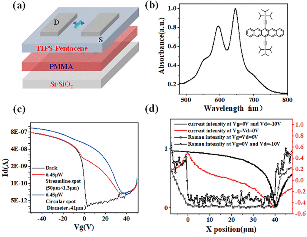 | ||
| Fig. 1 (a) Schematic diagram of the device structure of OFET (green bar represents a linear light spot schematic diagram, and blue arrow represents the scanning direction and the polarization direction of the laser). (b) Absorption spectrum of TIPS-pentacene thin film. The inset shows the molecular structure of TIPS-pentacene. (c) Transfer characteristic curve of TIPS-pentacene under dark state and light irradiation (entire channel photoresponse and micro area photoresponse and Vd = −50 V). (d) Normalized Raman intensity (1557 cm−1) and micro region photocurrent (with and without external electric field) as a function of excitation position. | ||
In order to study the photoresponse difference between the entire channel excitation and local excitation in OFETs, we focused the laser into different shapes of light spots and irradiated them on the channel under the same light intensity (6.45 μW). Fig. 1(c) compares the transfer curves of TIPS-pentacene under dark state and different light states. Under the excitation of such a low-power laser, it can be assumed that the absorption of light by organic semiconductors is the same. Both irradiation methods can generate good photoresponse, with the threshold voltage drifting in the forward direction and the degree of drift being basically the same (Vth = 35 V), indicating that the number of charges separated and accumulated minority charge carriers in OFETs is basically the same. However, the current rise is different: in the experiment of micro region photoresponse, there is a significant slowdown in the later stage of current rise, which may be due to the higher local charge density and strong recombination effects in the micro region.
Compared with Raman spectroscopy mapping, micro region photocurrent technology has better sensitivity and in situ monitoring performance. Fig. 1(d) compares the in situ spectra of Raman scattering collected from OFET channels and synchronously records the micro region photocurrent. The Raman intensity at 1557 cm−1 (Fig. S2, ESI†) was selected as the Z coordinate, which corresponds to the C–C stretch of TIPS-pentacene.45 Regardless of whether additional gate voltage and source drain voltage were added, there was no significant change in Raman intensity along the channel, indicating that with Raman imaging technology it is difficult to observe potential changes at different positions of the device.
On the contrary, when gate voltage and/or source drain voltage is added, the micro region photocurrent spectrum can indicate significant changes in photocurrent at different positions of the channel. There are two independent decay processes in the micro region photocurrent under different drain voltage. When the source drain voltage is not zero, there is a slow decay process, which theoretically corresponds to the potential distribution at different positions in the FET channel. We have discussed this process in detail in our previous work.41,46
When the source drain voltage is zero, the micro region photocurrent rapidly reaches its maximum value and decays rapidly near the electrodes. This process is completed within a distance of several micrometers. It is very similar to an inorganic system and can contain important carrier diffusion information.19 The antisymmetric spectral type is an important characteristic of minority carrier motion. In the process of the free diffusion of minority carriers to different directions of the device, due to the limited diffusion length, it can only be extracted by relatively nearby electrodes, so the current direction will be reversed at the position in the middle of the channel. In this article, we select the case where the source drain voltage is zero. Here, we mainly use two basic physical parameters to characterize the photocurrent in the micro region: one is the peak value of the photocurrent, and the other is the decay rate after the photocurrent reaches its peak value. The length at which the photocurrent decays to 1/e of its maximum value is defined as the apparent minority charge carrier diffusion length (LD); then:
 | (2) |
Considering the resolution limit of the instrument, the lateral spatial resolution can be calculated using:
| d = 1.22λ/NA | (3) |
When the gate voltage and source drain voltage are both 0 V, the electrode is only used to collect freely diffused photogenerated carriers without applied voltage, which reflects the diffusion characteristics of the intrinsic carriers. The micro region photocurrent exhibits an antisymmetric structure. The absolute value of the photocurrent at the edge of the electrode is the highest, with positive and negative current having been observed in the two electrodes respectively. As the excitation position moves away from the electrode towards the middle of the channel, the absolute value of the photocurrent gradually decreases. At the center of the channel, the photocurrent decreases to zero. These characteristics are the same as those with an inorganic material as the active layer, the photocurrent spectra of which are closely related to minority charge carriers.
2.1 Evidence for the key role of minority charge carriers in micro region photocurrent spectrum
The current behavior during the change of electrodes evidently demonstrates the importance of minority carrier migration in micro region photocurrent. The energy level structure diagram in the dark of a TIPS-pentacene-based OFET with Ag or Au electrodes is shown in Fig. 2(a). The work function (−5.1 eV) of the Au electrode is closer to the HOMO energy level (−5.2 eV) of TIPS-pentacene than that of the Ag electrode (−4.3 eV), which is more conducive to hole injection. Therefore, OFETs with Au electrodes tend to show better photoelectric performance. The transfer characteristic curves of Au and Ag electrode devices in the dark state are consistent with previous literature reports, indicating that devices with an Au electrode have better hole transport capabilities than with an Ag electrode. As shown in Fig. 2(b), when the gate voltage and source drain voltage are both −50 V, the saturation current with Ag electrode is only 0.73 μA, while that with Au electrode is 2.3 μA. The current on/off ratio also increased from 3.3 × 10⁵ to 1.05 × 10⁶. | ||
| Fig. 2 (a) Energy level diagram of TIPS-pentacene, Ag and Au. (b) Transfer characteristic curves of Ag electrode devices and Au electrode devices in the dark with Vd = −50 V. (c) Comparison diagram of micro region photocurrent between OFETs with Ag electrode device and Au electrode with Vd = Vg = 0 V. | ||
However, for the micro region photocurrent under zero drain voltage, the obtained results were completely different. The experimental results are shown in Fig. 2(c). In the OFET with Ag electrodes, the photocurrent increases greatly with the excitation position, with a peak current of 1.33 × 10⁻¹¹ A, while in the OFET with Au electrodes, only when the excitation position is at the edge of the electrode can a very small amount of photocurrent be collected (with a peak value of 7.72 × 10⁻¹³ A). This is difficult to explain by majority carriers of hole transport, since the work function of Au is more consistent with the HOMO energy level of TIPS-pentacene, but OFETs with Au electrodes show such a low micro region photocurrent response. This phenomenon is the best experimental evidence for the photoelectric current in the micro region being dominated by minority charge carriers. It can be explained specifically as follows: compared with the Au electrode, the work function of the Ag electrode is less different from the LUMO energy level of TIPS-pentacene, so it is easier for the minority charge carrier electrons diffused to the electrode to cross the barrier and be collected by the electrode, which can form a larger photocurrent together with hole carriers in reverse motion; on the contrary, the work function of the Au electrode is much more different from the LUMO energy level of TIPS-pentacene than that of Ag electrode, so it is more difficult for electrons to diffuse to the electrode. Although the initial aim of the electrode-dependence experiment was to introduce an Au electrode to obtain a higher current, the actual result was just the opposite. This phenomenon surprised us very much, and minority charge carriers seemingly can travel very long distances.
Besides, it is very interesting that the effect of gate voltage is small in the micro-area photocurrent experiment, although the gate voltage has a very large effect on the current in transistors. Firstly, for a device with zero gate voltage, or fabricated on quartz substrates without a gate, obvious micro-area photocurrent can be observed; further, with different gate voltage, the LD value will exhibit a certain change, as shown below, but this change is not as obvious as for different drain/source electrodes. This is probably because the gate voltage is mainly related to majority carriers. The small effect of gate voltage on the generation of micro-region photocurrent would also be good evidence for the minority control process.
2.2 Intrinsic carrier diffusion length from micro region photocurrent spectrum
The influence of optical effects on the measurement results is a very important factor; for example, Airy diffraction, optical waveguide, light scattering and other phenomena will cause the measurement results to be too large.33,34 In this work, we evaluated the influence of the above optical phenomena through different experimental conditions, especially experiments with different light intensities, and discussed the variation of LD values with electrical conditions.Defect density is an important factor affecting LD values.1–5 From the threshold voltage and subthreshold swing analysis of the transfer curve, the defect density of the whole polycrystalline film and the channel interface in the dark state is 2.1 × 1011 cm−2 and 2.8 × 10¹³ eV−1 cm−2, respectively. In order to better observe the intrinsic carrier diffusion, we use the method of repeated illumination to pretreat the intrinsic defects. As shown in Fig. 3(a), during repeated scanning of the same area of the device channel, the photocurrent maximum and decay rate are not completely the same. The photocurrent maximum of the first scan is the smallest, approximately 2 × 10⁻¹² A. As the scan times gradually increase, the photocurrents increase. With a scan number of 15, the photocurrent reaches its maximum value, with a peak value of about 1.8 × 10⁻¹¹ A, which indicated that the charge trap sites in polycrystalline film are filled step by step. After that, with increasing scan times, the photocurrent becomes stable. Corresponding to photocurrent maximum, the LD value gradually decreases with the increase of scanning times, and ultimately becomes stable, with a value near 2.2 μm, as shown in Fig. 3(b). It would be a strange phenomenon that the LD value decreases with defect structure decrease. Since the photocurrent is constantly increasing, the possibility of defect-induced current is ruled out. Here we mainly use experimental error to explain this phenomenon, which will be discussed in detail below. The most important point is that the prefilling of the charge trap can build a quasi-trap-free mode with stable photocurrent and LD value, which is beneficial for the measurement of basic physical parameters. In the following text, preprocessing for stable photocurrent value is carried out before the formal experiment to avoid experimental errors caused by charge trap sites.
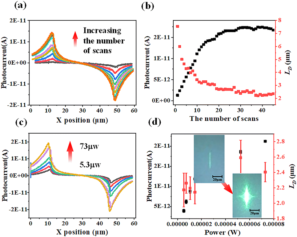 | ||
| Fig. 3 (a) Micro region photocurrent spectra of the device at the same position with different scanning times. (b) The maximum photocurrent and the fitted LD value as a function of the scan times. (c) Micro region photocurrent spectra as a function of light intensity. (d) The maximum photocurrent and fitted LD values as a function of laser power (insets compare CCD images of the laser spot at different laser power). The maximum photocurrent and LD value are the average of the results obtained from 10 parallel experiments. | ||
Laser power is an important factor affecting the magnitude of micro region photocurrent. In order to find a suitable laser power that does not damage the organic semiconductor and can afford accurate experimental results, the photocurrent spectra as a function of laser power are checked as shown in Fig. 3(c). Generally, the photocurrent gradually increases with the increase of laser power. When the laser power increases from 5.26 μW to 14.6 μW, the photocurrent linearly increases rapidly from 3.92 × 10⁻¹² A to 2.11 × 10⁻¹¹ A, and then when the laser power is increased, the scattering effect between charge carriers is significantly enhanced, and the increasing trend of photocurrent becomes slow, which determines the linear response of laser power between 5.26 μW and 14.6 μW.
Fig. 3(d) shows the relationship between the minority charge carrier diffusion length LD and laser power. When the laser power is less than 1.79 × 10⁻⁵ W, the LD value remains basically stable at different laser power, with a value of approximately 2.2 μm; when the laser power is larger than 1.79 × 10⁻⁵ W, the LD value increases to 2.6 μm. This is due to the decrease in spot quality with the increase of laser power (laser scattering to both sides). The insets of Fig. 3(d) show CCD images of the linear spot at low and high laser power. At high laser power, the extension of the linear laser spot to both sides reduces the resolution and leads to an increase in the LD measurement value. Rui et al.19 also pointed out that when using micro region photocurrent technology to measure the LD value, light interference and photothermal effect would affect the accuracy of the LD value. Therefore, when using micro region photocurrent technology to measure LD values, low laser power and high-quality light spots should be selected, which will greatly increase the accuracy of experimental results.
As shown in Fig. S3 (ESI†), the laser wavelength, exposure time, scanning direction, and different scanning steps all have varying degrees of influence on the values of micro region photocurrent and LD. Besides laser intensity, all other cases follow the rule that a larger photocurrent is related to a smaller LD. In most cases, we want to use physical mechanisms to explain the observed phenomena, but in this system, the current value is relatively small, and the influence of experimental error is greater. From the previous analysis, it can be explained that: (1) the large LD value obtained when the photocurrent signal in the micro region is small, which is due to the easy introduction of fitting errors, and on the other hand, for the low charge carrier density at this time, the hindrance of photogenerated electrons is relatively small, resulting in a larger charge carrier diffusion distance. (2) When the value of micro region photocurrent increases, the interaction between carriers hinders the diffusion of photogenerated carriers; in particular, conditions that increase the photocurrent often increase the number of photogenerated carriers, which leads to the LD value decreasing. Therefore, we believe that only the relatively constant LD value under certain conditions is meaningful. In addition, it should be emphasized that the test is based on very good device working conditions and very low defect density; otherwise, the device dark current is already very large, which is difficult to fit and analyze.
2.3 The possible reason for the micron-level minority charge carrier diffusion length
The LD in all experimental devices tends to a large, fixed value between 2.1 and 2.5 μm, although the maximum value of the micro photocurrent in these devices may vary greatly, and the width/length of the channel are not exactly the same. As discussed above, this is a value that is much larger than the spectral resolution, and should be credible. To our knowledge, possible systematic errors would mainly come from the additional exciton diffusion. The measured LD value of the photoexcitation experiment should include the exciton diffusion length and the charge carrier diffusion length after exciton splitting, which is larger than the charge carrier diffusion length only (Fig. 4). Nevertheless, it is reported that the exciton diffusion length of TIPS-pentacene material is very small: on the one hand, the triplet state diffusion length of the crystal film and amorphous film is estimated to be ∼75 nm and ∼14 nm, respectively, which is much smaller than the length we measured;36,47 on the other hand, the diffusion length of the triplet exciton should be longer than that of the singlet state. Therefore, the apparent diffusion length observed in the experiment is mainly contributed by the carrier diffusion, which would be much larger than those of both triplet and singlet excitons. Besides, theoretical analysis also shows that even if there is a significant difference in the mobility of electrons and holes, when the mobility of minority charge carriers remains basically unchanged, the measured apparent diffusion length is slightly larger than the theoretical value.19 | ||
| Fig. 4 Schematic diagram of photogenerated carrier generation, relaxation and diffusion. During the whole process, excitons and photogenerated carriers undergo two structural relaxation processes. | ||
As shown in eqn (1), the mobility and lifetime of minority charge carriers together determine their diffusion length. A schematic diagram of photogenerated carrier generation, relaxation and diffusion is shown in Fig. 4. Although the mobility of organic molecules is relatively low, the long lifetime of intrinsic charge recombination is a typical character of organic conjugated materials with covalent bonds and vibrational relaxation.40 Recombination is difficult with a long lifetime, because the structure relaxes to an anionic polaron resulting in local energy minimums and metastable structures, and not easy to recombine by the majority charge carriers. This provides a good theoretical basis for the long intrinsic carrier diffusion length. In this work, we used a wide-channel transversal device and constructed a good carrier flow environment being trap-free for the observation of a micron-level charge carrier diffusion length. The micron-level charge carrier diffusion length is a very important parameter for expanding the application of organic semiconductors, and can help us understand why thick-film devices41–46 and long-channel devices can achieve good feasibility.32 It is worth emphasizing that the actual minority carrier lifetime has a strong relationship with the experimental conditions and device structure. For example,48–50 in a diode, minority carriers can migrate to the electrode very quickly and have a short minority carrier lifetime, but when the acceptor concentration in the system is very small, the charge movement is difficult and shows a very long minority carrier lifetime.
In addition, we use the way of light excitation to obtain charge carriers, and there may be a carrier penetration effect, which is also a possible reason for obtaining a very long diffusion length. Nevertheless, because the photoelectric process such as photovoltaic and light detection itself is also photoexcited, this conclusion is consistent with the application conditions, and can reflect the actual working state of the device.
During the experiment, we also tried bulk heterojunction systems with different structures, such as P3HT/ITIC, PM6 and so on, where the LD values obtained are all on the micron scale (Fig. S4, ESI†). More interesting, in bulk-heterojunction structures, the specific value varies greatly with different device structures and different experimental conditions. For example, in the P3HT/ITIC system, the micro region photocurrent is quite different when using different annealing temperatures, which indicate that micro region photocurrent and LD value would be very sensitive to experimental conditions. In our opinion, it would be more meaningful than the intrinsic transport process, which helps to optimize the device performance and in situ mechanism. These results will be discussed in detail in our future work.
2.4 The effect of external electric field on minority carrier diffusion
Further, we discuss the effect of an external electric field on minority charge carrier diffusion. As mentioned earlier, adding a horizontal source drain voltage will have an impact on the free diffusion of charge carriers in the one-dimensional direction, and there is a potential distribution in micro region photocurrent spectra. Here, we mainly discuss the influence of vertical electric field on the diffusion of charge carriers after introducing a gate voltage. Fig. 5(a) shows the micro region photocurrent spectra measured when different gate voltages are applied to the device when Vd is 0 V. The introduction of a gate voltage does not change the basic trend of the micro region photocurrent spectra. That is, no matter how much gate voltage is applied to OFETs, their micro region photocurrent shows the maximum at the edge of the electrode, and as the excitation position moves away from the electrode, the micro region photocurrent rapidly decays exponentially. | ||
| Fig. 5 (a) Micro region photocurrent plots at different Vg when Vd = 0 V. (b) Relationship between the fitted apparent LD and applied voltage. | ||
Under different gate voltages, the magnitude and attenuation degree of micro region photocurrent vary with distance. When a positive gate voltage is applied to the device, the device is in depletion mode. As the gate voltage increases, the micro region photocurrent gradually decreases. When the gate voltage increases from 0 V to 30 V, the micro region photocurrent decreases from 4.7 × 10⁻¹¹ A to 3.1 × 10⁻¹¹ A. Similar to the previous pattern, the LD value gradually increases, as shown in Fig. 5(b). When the gate voltage is 30 V, the fitted LD value can reach up to 4.5 μm. This is twice the value measured under other gate voltage conditions, and its variance is large, so it is highly likely due to the fitting error caused by the small micro region photocurrent. On the contrary, under negative gate voltage, the device has already turned on in the dark state. Here, we only choose the condition of Vg = −10 V, and the effect of dark current is not significant. Interestingly, in the cumulative mode, not only is the micro region photocurrent at its maximum, but LD also slightly increases, contrary to the previous pattern. Due to the high current in this region, the experimental repeatability is good, and the error is small. This increase value truly reflects the influence of conductive channel formation on charge carrier diffusion in the cumulative mode. It is generally believed that the mobility and lifetime of carriers in field effect transistors will increase, and the increase of LD value under field effect can be well explained by combining with eqn (1). The mobility and lifetime of minority charge carriers in situ are usually difficult to measure: the mobility of minority charge carriers cannot be measured when the majority carriers dominate; in order to obtain sufficient transient photocurrent, minority lifetimes are obtained under strong light intensity. The LD values obtained by using the micro region photocurrent spectrum can reflect the transmission characteristics of minority charge carriers more accurately, truly and comprehensively.
3 Conclusions
In this article, we elucidate a fundamental phenomenon observed through micro region photocurrent spectroscopy in TIPs-pentacene-based systems. Specifically, we demonstrate a unique photocurrent decay process occurring within microns of the electrode, characterized by an exceptional carrier diffusion length of 2.2 micrometers. By modulating various experimental conditions, we conclusively establish the correlation between the micro region photocurrent spectrum and the minority charge carrier diffusion length. Additionally, we delve into possible mechanisms underlying this remarkable behavior, offering insights into the structural and dynamic factors that contribute to the micron-level diffusion length.These findings not only enhance our understanding of the exceptional performance of organic semiconductors in thick-film and long-channel devices but also inspire innovative approaches to the design of organic semiconductor device structures. By exploring the intricate interplay between photocurrent spectra, carrier dynamics, and device architecture, we pave the way for the development of more efficient and versatile organic electronic systems.
Data availability
The data supporting this article have been included as part of the ESI.†Conflicts of interest
There are no conflicts to declare.Acknowledgements
This work was supported by the National Natural Science Foundation of China (52273178, 52373178, 21975076) and Natural Science Foundation of Guangdong Province (2023B1212060003).References
- M. C. Putnam, D. B. Turner-Evans, M. D. Kelzenberg, S. W. Boettcher, N. S. Lewis and H. A. Atwater, Appl. Phys. Lett., 2009, 95, 163116 CrossRef.
- A. Soudi, P. Dhakal and Y. Gu, Appl. Phys. Lett., 2010, 96, 253115 CrossRef.
- C.-J. Kim, H.-S. Lee, Y.-J. Cho, K. Kang and M.-H. Jo, Nano Lett., 2010, 10, 2043–2048 CrossRef CAS PubMed.
- T. Dittrich, F. Lang, O. Shargaieva, J. Rappich, N. H. Nickel, E. Unger and B. Rech, Appl. Phys. Lett., 2016, 109, 073901 CrossRef.
- C. Gutsche, R. Niepelt, M. Gnauck, A. Lysov, W. Prost, C. Ronning and F.-J. Tegude, Nano Lett., 2012, 12, 1453–1458 CrossRef CAS PubMed.
- G. K. Wehner, J. Appl. Phys., 1955, 26, 1056–1057 CrossRef CAS.
- J. Marek, J. Appl. Phys., 1984, 55, 318–326 CrossRef CAS.
- J. E. Allen, E. R. Hemesath and L. J. Lauhon, Nano Lett., 2009, 9, 1903–1908 CrossRef CAS PubMed.
- Y. Gu, J. P. Romankiewicz, J. K. David, J. L. Lensch and L. J. Lauhon, Nano Lett., 2006, 6, 948–952 CrossRef CAS.
- J. K. Hyun and L. J. Lauhon, Nano Lett., 2011, 11, 2731–2734 CrossRef CAS PubMed.
- M. Burghard and A. Mews, ACS Nano, 2012, 6, 5752–5756 CrossRef CAS PubMed.
- M. Barkelid, G. A. Steele and V. Zwiller, Nano Lett., 2012, 12, 5649–5653 CrossRef CAS PubMed.
- Y. H. Ahn, A. W. Tsen, B. Kim, Y. W. Park and J. Park, Nano Lett., 2007, 7, 3320–3323 CrossRef CAS PubMed.
- E. J. H. Lee, K. Balasubramanian, R. T. Weitz, M. Burghard and K. Kern, Nat. Nanotechnol., 2008, 3, 486–490 CrossRef CAS PubMed.
- J. Park, Y. H. Ahn and C. Ruiz-Vargas, Nano Lett., 2009, 9, 1742–1746 CrossRef CAS PubMed.
- X. Xu, N. M. Gabor, J. S. Alden, A. M. van der Zande and P. L. McEuen, Nano Lett., 2010, 10, 562–566 CrossRef CAS PubMed.
- F. Xia, T. Mueller, R. Golizadeh-Mojarad, M. Freitag, Y.-M. Lin, J. Tsang, V. Perebeinos and P. Avouris, Nano Lett., 2009, 9, 1039–1044 CrossRef CAS PubMed.
- D. B. Strasfeld, A. Dorn, D. D. Wanger and M. G. Bawendi, Nano Lett., 2012, 12, 569–575 CrossRef CAS PubMed.
- R. Xiao, Y. Hou, M. Law and D. Yu, J. Phys. Chem. C, 2018, 122, 18356–18364 CrossRef CAS.
- D. Yang and D. Ma, Adv. Opt. Mater., 2019, 7, 1800522 CrossRef.
- S. Allard, M. Förster, B. Souharce, H. Thiem and U. Scherf, Angew. Chem., Int. Ed., 2008, 47, 4070–4098 Search PubMed.
- K. J. Baeg, M. Binda, D. Natali, M. Caironi and Y. Y. Noh, Adv. Mater., 2013, 25, 4267–4295 CrossRef CAS PubMed.
- J. Tao, D. Liu, Z. Qin, B. Shao, J. Jing, H. Li, H. Dong, B. Xu and W. Tian, Adv. Mater., 2020, 32, 1907791 CrossRef CAS PubMed.
- Z. Zhong, L. Bu, P. Zhu, T. Xiao, B. Fan, L. Ying, G. Lu, G. Yu, F. Huang and Y. Cao, ACS Appl. Mater. Interfaces, 2019, 11, 8350–8356 CrossRef CAS PubMed.
- Y. Yang, R. C. da Costa, M. J. Fuchter and A. J. Campbell, Nat. Photonics, 2013, 7, 634–638 CrossRef CAS.
- Y. Gao, T. P. Martin, A. K. Thomas and J. K. Grey, J. Phys. Chem. Lett., 2010, 1, 178–182 CrossRef CAS.
- J. Gao, A. K. Thomas, J. Yang, C. Aldaz, G. Yang, Y. Qin and J. K. Grey, J. Phys. Chem. C, 2015, 119, 8980–8990 CrossRef CAS.
- M. Fiebig, C. Erlen, M. Göllner, P. Lugli and B. Nickel, Appl. Phys. A:Mater. Sci. Process., 2009, 95, 113–117 CrossRef CAS.
- C. H. Kim, Y. Bonnassieux and G. Horowitz, IEEE Trans. Electron Devices, 2013, 60, 280–287 CAS.
- A. Tsen, F. Cicoira, G. Malliaras and J. Park, Appl. Phys. Lett., 2010, 97, 023308 CrossRef.
- C. Liewald, D. Reiser, C. Westermeier and B. Nickel, Appl. Phys. Lett., 2016, 109, 053301 CrossRef.
- A. Giannopoulou and P. Kounavis, Org. Electron., 2018, 58, 167–177 CrossRef CAS.
- D. Kabra, S. Shriram, N. S. Vidhyadhiraja and K. S. Narayan, J. Appl. Phys., 2007, 101, 064510 CrossRef.
- U. Bothra, N. Jain, A. C. Y. Liu, A. Kala, W. Huang, X. Jiao, E. Gann, V. G. Achanta, C. R. McNeill and D. Kabra, ACS Appl. Nano Mater., 2020, 3, 11080–11089 CrossRef CAS.
- L. Smilowitz, N. S. Sariciftci, R. Wu, C. Gettinger, A. J. Heeger and F. Wudl, Phys. Rev. B:Condens. Matter Mater. Phys., 1993, 47, 13835–13842 CrossRef CAS PubMed.
- Z. Wang, H. Jiang, X. Liu, J. Liang, L. Zhang, L. Qing, Q. Wang, W. Zhang, Y. Cao and J. Chen, J. Mater. Chem. A, 2020, 8, 7765–7774 RSC.
- J. Chen, L. Zhang, X. Jiang, K. Gao, F. Liu, X. Gong, J. Chen and Y. Cao, Adv. Energy Mater., 2017, 7, 1601344 CrossRef.
- W. Gao, Q. An, M. Hao, R. Sun, J. Yuan, F. Zhang, W. Ma, J. Min and C. Yang, Adv. Funct. Mater., 2020, 30, 1908336 CrossRef CAS.
- Y. Zhang, H. Feng, L. Meng, Y. Wang, M. Chang, S. Li, Z. Guo, C. Li, N. Zheng, Z. Xie, X. Wan and Y. Chen, Adv. Energy Mater., 2019, 9, 1902688 CrossRef CAS.
- Y. Chang, X. Zhu, K. Lu and Z. Wei, J. Mater. Chem. A, 2021, 9, 3125–3150 RSC.
- M. Shou, Q. Zhang, H. Li, S. Xiong, B. Hu, J. Zhou, N. Zheng, Z. Xie, L. Ying and L. Liu, Adv. Opt. Mater., 2021, 9, 2002031 CrossRef CAS.
- S. K. Park, T. N. Jackson, J. E. Anthony and D. A. Mourey, Appl. Phys. Lett., 2007, 91, 063514 CrossRef.
- M. T. Lloyd, A. C. Mayer, A. S. Tayi, A. M. Bowen, T. G. Kasen, D. J. Herman, D. A. Mourey, J. E. Anthony and G. G. Malliaras, Org. Electron., 2006, 7, 243–248 CrossRef CAS.
- J. E. Anthony, J. S. Brooks, D. L. Eaton and S. R. Parkin, J. Am. Chem. Soc., 2001, 123, 9482–9483 CrossRef CAS PubMed.
- C.-W. Huang, X. You, P. J. Diemer, A. J. Petty, J. E. Anthony, O. D. Jurchescu and J. M. Atkin, Commun. Chem., 2019, 2, 22 CrossRef.
- H. Li, C. Wang, M. Shou, Y. Lin, X. Hou, Z. Xie and L. Liu, ACS Appl. Electron. Mater., 2021, 3, 1920–1930 CrossRef CAS.
- C. Grieco, G. S. Doucette, R. D. Pensack, M. M. Payne, A. Rimshaw, G. D. Scholes, J. E. Anthony and J. B. Asbury, J. Am. Chem. Soc., 2016, 138, 16069–16080 CrossRef CAS PubMed.
- L. Li, F. Zhang, J. Wang, Q. An, Q. Sun, W. Wang, J. Zhang and F. Teng, Sci. Rep., 2015, 5, 9181 CrossRef CAS PubMed.
- L. Li, F. Zhang, W. Wang, Y. Fang and J. Huang, Phys. Chem. Chem. Phys., 2015, 17, 30712–30720 RSC.
- W. Wang, F. Zhang, H. Bai, L. Li, M. Gao, M. Zhang and X. Zhan, Nanoscale, 2016, 8, 5578–5586 RSC.
Footnotes |
| † Electronic supplementary information (ESI) available. See DOI: https://doi.org/10.1039/d4tc05280c |
| ‡ Di Sun and Xuehua Hou contributed equally to this work. |
| This journal is © The Royal Society of Chemistry 2025 |