
Effect of channel patterning precision on the performances of vertical OECTs†
Ruhua
Wu
 a,
Chufeng
Wu
a,
Jinhao
Zhou
a,
Liang-Wen
Feng
b,
Jianhua
Chen
c,
Dan
Zhao
*a and
Wei
Huang
*a
a,
Chufeng
Wu
a,
Jinhao
Zhou
a,
Liang-Wen
Feng
b,
Jianhua
Chen
c,
Dan
Zhao
*a and
Wei
Huang
*a
aSchool of Automation Engineering, University of Electronic Science and Technology of China (UESTC), 611731, Chengdu, China. E-mail: danzhao@uestc.edu.cn; whuang@uestc.edu.cn
bKey Laboratory of Green Chemistry & Technology, Ministry of Education, College of Chemistry, Sichuan University, Chengdu, 610065, China
cDepartment of Chemical Science and Technology, Yunnan University, Kunming, China
First published on 7th March 2025
Abstract
Precise patterning of electronic functional layers is vital for integrated electronics, where high integration density is required. Similarly, for organic electrochemical transistors (OECTs), the patterning precision of the channel layer is essential for device miniaturization, parasitic capacitance reduction, and accurate performance evaluation. In particular, for an emerging OECT architecture, vertical OECT (vOECT), the effect of patterning precision on key device parameters (such as transconductance (gm) and transient time (τ)) remains unclear. Here, controllable patterning of vOECT channel regions is realized by direct laser etching, where 2–100 μm margin lengths (lM) are left beyond the vertical channel area. By quantitatively analyzing the impact of margin areas on device performance (including drain currents (ID), gm, and τ), it has been found that a larger lM leads to significantly increased ID and gm in both n- and p-type OECTs (106.94% and 61.46% enhancement of ID and 102.92% and 92.59% enhancement of gm in n- and p-type OECTs, respectively, are observed as lM increases), which saturate under an lM of ∼60 μm. Nevertheless, linearly increasing τ (from hundreds of microseconds to a few milliseconds) is observed with increasing lM, revealing that parasitic capacitance outside the channel would result in a longer redox reaction time but not always higher ID and gm. It is revealed that the patterning precision of active layers alters the OECT performances tremendously and can be designed to meet different application requirements (either high amplification capability, high integrating density, or fast response time) in OECT-based electronics.
 Wei Huang | Wei Huang obtained his B.S. in physics from Nankai University and his Ph.D. in optical engineering from the University of Electronic Science and Technology of China (UESTC). He was a research assistant professor at Northwestern University, under the supervision of Professor Tobin J. Marks and Professor Antonio Facchetti. Currently, he is a Professor at the School of Automation Engineering, UESTC. His research interests include flexible/stretchable electronics, neuromorphic electronics, and transistor-based chemical/biological sensors. |
Introduction
Organic electrochemical transistors (OECTs), consisting of organic mixed ionic–electronic conductor (OMIEC)-based channels, exhibit mixed ionic and electronic coupling and transport capabilities.1–3 Therefore, exceptionally high transconductances (gm, >10 mS) can be acquired in OECTs due to large volumetric capacitance (>10 F cm−3) by ion doping into the channel, making them ideal for biosensors with simultaneous sensing and amplification capabilities.4–6 Moreover, OECTs can be further integrated into complementary logic circuits with good biocompatibility and biomimetic properties,7–11 which can be further applied in next-generation neuromorphic electronics and brain–computer interfaces.12–15 The performances of OECTs can be improved through various methods, including polymer backbone design and side-chain engineering,16–18 gate/electrolyte or channel/electrolyte interface optimization,19–21 and device structural innovation.22–24In particular, by introducing a vertical device geometry, vertical OECTs (vOECTs), which are distinct from the conventional planar OECTs (cOECTs), demonstrated a reduced channel length (OMIEC film thickness) of less than ∼100 nm, an enhanced gm of 0.2–0.4 S, an on/off current ratio (Ion/Ioff) of ∼107, a transient time (τ) of less than 1 ms, and ultra-high cycling stability (>50![[thin space (1/6-em)]](https://www.rsc.org/images/entities/char_2009.gif) 000 cycles).22,25,26 Such high transistor performances rely on a transistor channel with photopatterning capability by mixing OMIECs with photo crosslinkers. Moreover, precise and well-defined OMIEC patterning not only facilitates device integration, enhances integration density, and reduces crosstalk, but also significantly impacts the performances of individual devices, including gm, Ion/Ioff, etc.27–29 For instance, Enrico et al.30 demonstrated that by using femtosecond laser microfabrication to pattern the encapsulation and OMIEC layers of cOECTs, a significantly shortened τ (from hundreds of milliseconds to hundreds of microseconds) was achieved. Moreover, research on the patterning of semiconductor layers in planar thin-film transistors (TFTs) has shown that precise patterning of the active region would contribute to better transient performances.31,32 Even though a previous study revealed that the contact area in planar OECTs would also affect the transistor dynamic characteristics,32 for vOECTs, studies that provide a quantitative analysis of the impact of patterning precision on the performance metrics are still missing. Providing such a correlation between device performance and channel patterning precision would be extremely valuable to guide the design, fabrication, and optimization of vOECT-based electronics.
000 cycles).22,25,26 Such high transistor performances rely on a transistor channel with photopatterning capability by mixing OMIECs with photo crosslinkers. Moreover, precise and well-defined OMIEC patterning not only facilitates device integration, enhances integration density, and reduces crosstalk, but also significantly impacts the performances of individual devices, including gm, Ion/Ioff, etc.27–29 For instance, Enrico et al.30 demonstrated that by using femtosecond laser microfabrication to pattern the encapsulation and OMIEC layers of cOECTs, a significantly shortened τ (from hundreds of milliseconds to hundreds of microseconds) was achieved. Moreover, research on the patterning of semiconductor layers in planar thin-film transistors (TFTs) has shown that precise patterning of the active region would contribute to better transient performances.31,32 Even though a previous study revealed that the contact area in planar OECTs would also affect the transistor dynamic characteristics,32 for vOECTs, studies that provide a quantitative analysis of the impact of patterning precision on the performance metrics are still missing. Providing such a correlation between device performance and channel patterning precision would be extremely valuable to guide the design, fabrication, and optimization of vOECT-based electronics.
Here, vOECTs based on n-type poly(benzimidazobenzophenanthroline) (BBL) and p-type poly(2,5-dipentaethyleneglycol-3,6-di(thiophen-2-yl)-2,5-dihydropyrrolo[3,4-c]pyrrole-1,4-dione-alt-2,5-bis(3-triethyleneglycoloxythiophen-2-yl)) (gDPP-g2T) as the channel OMIECs (Fig. S1†) are fabricated and characterized to examine the effects of channel patterning precision on the transistor's static and dynamic performances. A picosecond direct laser writing (DLW) system is applied to precisely pattern the BBL-based channel, achieving a patterning resolution and alignment accuracy of <2 μm. Consequently, by increasing the margin length (lM) of the OMIEC pattern from 2 μm to 100 μm for BBL-based vOECTs (Fig. 1), Ion and Ioff increase from 0.36 ± 0.01 mA and 0.75 ± 0.11 nA to 0.72 ± 0.86 mA and 4.81 ± 0.97 nA, respectively. Meanwhile, τon (turn-on transient time) and τoff (turn-off transient time) grow from 2.16 ± 0.11 and 0.43 ± 0.07 ms to 7.64 ± 0.93 and 1.60 ± 0.17 ms, respectively, as lM increases from 2 to 100 μm. Similar trends on these key parameters are also observed in p-type gDPP-g2T-based vOECTs. Specifically, Ion increases with the expanded lM and reaches a plateau, which can be well-fitted by employing a fringing effect model, while Ioff is dominated by the channel capacitance, following a quadratic function concerning lM. On the other hand, τ exhibits an approximately linear trend depending on lM, which agrees with that in the Bernards model.33 This work indicates that a larger margin region beyond the effective channel area contributes to additional Ion and gm due to parasitic currents, but slower device response due to larger volume capacitance. Consequently, a quantitative relationship between vOECT performance and channel patterning precision is established, which provides guidelines for the optimal demand-oriented design of bioelectronics with either high amplification capability (high gm), fast response (short τ), or dense integration.
 | ||
| Fig. 1 (a) Fabrication flow diagrams of a DLW patterned vOECT, (i) bottom electrode deposition and patterning, (ii) OMIEC channel spin-coating and patterning, (iii) top electrode deposition, and (iv) encapsulation layer deposition and patterning. (b) Schematic of a vOECT and definition of the margin length (lM). (c) Microscopy images of the BBL-based vOECTs with different patterning precisions (scale bar = 100 μm). | ||
Results and discussion
n-Type vOECTs were fabricated on 1 mm thick glass substrates by vertically stacking a bottom Au electrode, a DLW-patterned BBL film, a top Au electrode, and an encapsulation layer (Fig. 1a). The detailed fabrication process can be found in the Experimental section, where vOECTs with approximately 100 nm thick BBL (Fig. S2 and Table S1†) sandwiched between top (drain) and bottom (source) electrodes with the same electrode width (WT and WB) of 30 μm were fabricated. In particular, the OMIEC films were patterned within different lM of 2, 5, 10, 20, 40, 60, 80, and 100 μm, respectively, beyond the overlapping effective channel region, where the encapsulation layer has the same opening size as that of the patterned OMIEC film (Fig. 1b, c and S3†). The DLW process effectively ensures patterning and alignment precision between the bottom electrode and the semiconductor film within 2 μm.The transfer, gm, and subthreshold swing (SS) characteristics of the vOECTs based on BBL with varied lM are demonstrated in Fig. 2a–c, where ID, gate current (IG), and gm exhibit obvious increasing trends as lM expands. It should be noted that due to the geometric symmetry of the vOECT, selecting either the top or bottom electrode as the source or drain electrode would not significantly affect device performances (Fig. S4†). At the same time, the lowest SS remains relatively unchanged at approximately 65 mV dec−1 in all devices. Meanwhile, the slightly negatively shifted threshold voltage (Vth) with increasing lM suggests that more ionic injection pathways towards the channel and/or smaller electrode–channel interface resistance with a larger margin area may be formed (Fig. S5†). Specifically, as shown in Fig. 2d, Ion (ID under VG = 0.6 V and VD = 0.1 V) gradually increases from 0.36 ± 0.01, 0.47 ± 0.04, 0.51 ± 0.05, 0.62 ± 0.02 and 0.67 ± 0.03 mA with an lM of 2, 5, 10, 20, and 40 μm, respectively. Then, Ion reaches a plateau of ∼0.72 mA when lM is ≥60 μm. For IG, as the lM increases from 2 μm to 100 μm, an approximately two orders of magnitude increase in IG (from ∼10−9 A to 10−7 A at VG = 0.6 V and from 10–10 A to 10–8 A at VG = −0.2 V) is observed. Such a phenomenon indicates that, as enlarged lM leads to more margin areas other than the direct channel area (the overlapping area of top and bottom electrodes), pronounced ion injection/extraction behavior in the OMIEC channel would result in extra electron carrier transport paths between source/drain electrodes.
 | ||
| Fig. 2 (a–c) Transfer characteristics (VD = 0.1 V) on the log scale (a) and linear scale (forward scan only) (b), and plots of gm and SS of BBL-based vOECTs with varied lM. (d–g) Key parameters of Ion (d), gm (e), Ioff along with IG in the off-state (f), and the on/off ratio (g) of BBL-vOECTs as a function of lM (error bars represent the standard deviation of 5 individual vOECTs from 3 batches). | ||
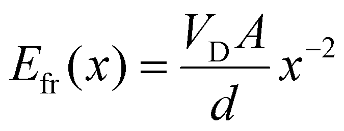
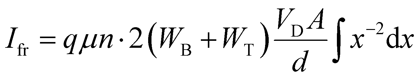
Next, a fringe field effect model, which has already been validated for its effectiveness in planar thin film transistors,34 is employed to fit the above ID variation. Here, the ID of vOECTs can be divided into two components, expressed by the following formula:
| ID = Ich + Ifr | (1) |
| J = qμn(r)E(r) | (2) |
 | (3) |
 | (4) |
 | (5) |
 | (6) |
Consequently, the data in Fig. 2d are fitted by combining eqn (1) and (6). It should be noted that this model only considers the OMIEC margin areas that make direct contact with the electrodes (areas ①–④, Fig. S6†) while disregarding the areas that are not making direct contact with the electrodes (areas ⑤–⑧, Fig. S6†). As shown in Fig. 2d, under such a model, a good fitting result is demonstrated with excellent agreement on the measured Ion. Furthermore, Fig. 2e illustrates peak gm of vOECTs with varied lM of 2, 5, 10, 20, 40, 60, 80, and 100 μm being 1.21 ± 0.03, 1.62 ± 0.14, 1.70 ± 0.14, 2.04 ± 0.12, 2.12 ± 0.11, 2.29 ± 0.13, 2.23 ± 0.08, and 2.39 ± 0.12 mS, respectively. The gm variation concerning lM corresponds to that of Ion, exhibiting sharp growth followed by a plateauing trend. This suggests that the parasitic current effect in the redundant OMIEC region predominantly contributes to this portion of gm.
Compared to Ion, the increase in the Ioff of vOECTs is more apparent, which rises from 0.75 ± 0.11 nA to 4.81 ± 0.97 nA as lM increases from 2 to 100 μm. According to the current discrete model, ID (Ioff) is composed of two parts: ICH and IGD.36–38 In the off-state of vOECTs, ICH contributes little to ID due to the negligible conductivity of pristine BBL.39 Thus, Ioff is dominated by the portion of IGD (Fig. S8†). Based on the variation in IG during the off-state of the OECT, it can be observed that they are proportional to the OMIEC redundant area between the electrolyte and the channel, exhibiting a quadratic relationship concerning lM (Fig. 2f). It is concluded that IG is primarily dominated by the volume capacitance of the channel, which is reflected by the ionic doping/dedoping currents.28 Furthermore, the electrolyte–gold electrode contact has been demonstrated to affect the performance of the vOECT, particularly the Ioff (Fig. S9 and S10†). Therefore, accurate patterning of the OMIEC channel is beneficial for improved Ion/Ioff ratios (Fig. 2g). As the lM decreases from 100 μm to 20 μm, the Ion/Ioff ratio of the BBL-based vOECT increases from (1.53 ± 0.28) × 105 to (7.00 ± 0.51) × 105. It should be noted that further reducing lM causes an abnormal increase in Ion/Ioff, which is due to possible short circuits between the top and bottom electrodes as shorter lM may lead to imperfect gapping between electrodes, resulting in a slight decrease in Ion/Ioff for more precisely patterned vOECTs (lM < 10 μm).
To validate the transistor performance variation trend affected by channel patterning precision, p-type gDPP-g2T-based vOECTs are also fabricated and characterized with different lM. It should be noted that a photolithography patterning process is employed by mixing gDPP-g2T with a photo-crosslinker (double-end trifluoromethyl diazirine (DtFDA)). Here, p-type thin films with a thickness of ∼124 nm and an lM of 5 to 100 μm are fabricated (Fig. S2, S11–12 and Table S1†). The transfer characteristics of the p-type OECT are shown in Fig. 3a, where the SS and Vth remain relatively constant with varying lM, with values of 95.44 ± 1.08 mV dec−1 and −0.30 ± 0.01 V, respectively (Fig. 3b and c). As lM increases from 5 μm to 100 μm, Ion increases from 3.42 ± 0.11 to 5.67 ± 0.24 mA, which can be fitted using the fringe field model (Fig. 3d). Similarly, gm increases from 13.36 ± 0.49 mS to 20.08 ± 1.45 mS as lM increases from 5 μm to 100 μm (Fig. 3e), while Ioff increases from 12.76 ± 1.41 to 157.78 ± 20.08 nA, demonstrating a trend similar to that in n-type vOECTs, which fits well with a quadratic function of lM, indicating proportionality to the patterned area (channel capacitance) (Fig. 3f). Furthermore, the effect of patterning on Ion/Ioff follows the same trend as that observed in the n-type OECT. As lM increases from 5 μm to 100 μm, Ion/Ioff decreases from (2.70 ± 0.28) × 105 to (0.36 ± 0.05) × 105 (Fig. 3g). These results confirm the assumptions for n-type OECTs and indicate that the impact of semiconductor patterning on device performance is independent of the type of charge carrier.
 | ||
| Fig. 3 (a–c) Transfer characteristics (VD = −0.1 V) on the log scale (a) and linear scale (forward scanning only) (b), and plots of gm and SS of vOECTs with a gDPP-g2T channel with varied lM. (d–g) Key parameters of Ion (d), gm (e), Ioff along with IG in the off-state (f), and the on/off ratio (g) of gDPP-g2T-vOECTs as a function of lM (error bars represent the standard deviation of 5 individual vOECTs from 3 batches). | ||
Additionally, the impacts of patterned precision on the transient characteristics of the vOECTs are investigated. Fig. 4a shows the transient curves of the n-type vOECTs with lM varying from 2 μm to 100 μm. It should be noted that the applied input pulses (VGS) exhibit a spike width of 0.1 s and an amplitude from −0.3 V to 0.5 V, along with a VDS of 0.1 V. The extracted τ are presented in Fig. 4b and c, where τon and τoff increase from 2.16 ± 0.11 ms and 0.43 ± 0.07 ms to 7.64 ± 0.93 ms and 1.60 ± 0.17 ms, respectively, as lM increases from 2 μm to 100 μm. Both τon and τoff exhibit an approximately linear relationship with lM. According to the ionic circuit that describes the ionic transition in the electrolyte of OECTs, the τ of OECTs is related to the solution resistance (RS) and channel capacitance (CCH) (Fig. S13(i)†).38 Imperfectly patterned regions of the BBL can generate parasitic capacitance (CPr), leading to variations in the transient response time of vOECTs. Considering the influence of CPr, the ionic circuit is transformed into Fig. S13(ii),† where  . From the electrochemical impedance spectroscopic (EIS) measurement (Fig. S14†) of the vOECTs, where the corresponding values of
 000 cycles, while the values of gm are 89.42%, 88.76%, and 86.33%. However, the increase in Ioff is significantly more pronounced in the vOECT with lM = 5 μm compared to devices with larger patterns. This suggests that electrochemical reactions at the film edges may exacerbate structural variations in the polymer impairing the device's off-state performance.
 | ||
| Fig. 4 Transient response (a) and the plots of τon (b) and τoff (c) of n-type vOECTs as a function of lM. Transient response (d) and the plots of τon (e) and τoff (f) of p-type vOECTs as a function of lM (error bars represent the standard deviation of 5 individual vOECTs from 3 batches). | ||
Conclusions
In this work, the key performance metrics of both n- and p-type vOECTs, including Ion, Ioff, gm, Ion/Ioff, and τ for patterning precision, have been investigated by adopting DLW for n-type OMIECs and photopatterning for p-type ones. It is revealed that the expansion of lM enhances the Ion and gm of vOECTs but also leads to higher Ioff and longer τ. As lM increases, Ion and gm increase significantly and saturate with lM > 40 μm. A fringe field model considering parasitic currents from the OMIEC that makes direct contact with the source/drain electrode outside the channel area shows good fitting to experimental trends. Additionally, an increase is observed in Ioff and IG, following a quadratic relationship with lM, which is attributed to the additional margin areas that introduce higher channel capacitance and an additional leakage path. Moreover, channel patterning precision also influences the dynamic performance of vOECTs. As lM decreases, the τon and τoff of both n-type and p-type vOECTs are significantly reduced. This improvement in τ with a shorter lM is due to the less parasitic capacitance. These findings underscore the importance of patterning precision in the vOECT channel and provide guidance and reference for optimizing the performance of organic electronics based on OECTs.Experimental section
Materials
gDPP-g2T, DtFDA, and cinnamate-cellulose (Cin-Cell) were synthesized based on previous reports.22,40–42 SU-8 and the SU-8 developer were purchased from Wenhao Co., Ltd. BBL, isopropyl alcohol and chloroform were purchased from Sigma-Aldrich. Phosphate buffer saline (PBS) is supplied by Solarbio and used as the aqueous electrolyte.Solution preparation
gDPP-g2T and Cin-Cell were first dissolved in chloroform with a concentration of 20 mg mL−1, respectively. DtFDA was dissolved in chloroform with a concentration of 100 mg mL−1. These solutions were stirred at room temperature overnight. Solutions for the p-type channel layers were prepared by mixing the solution gDPP-g2T with the solution of DtFDA and Cin-Cell to yield a weight ratio of 10:1:6. A blend solution of 20 mg mL−1 Cin-Cell and 100 mg mL−1 DtFDA with a weight ratio of 4:1 was prepared for the precursor of the encapsulation layer. A solution for the n-type channel layers was prepared by solving BBL in methanesulfonic with a concentration of 20 mg mL−1.
vOECT fabrication
:DtFDA:Cin-Cell = 10:1:6 in the weight ratio) was spin-coated at 3000 rpm for 30 s. The gDPP-g2T thin films were then cross-linked by exposure to 365 nm UV for 3 min and 285 nm UV for 2 min with a photomask, followed by developing in chloroform for ∼3 s and blow drying. The 150 nm Au top electrode was thermally evaporated at a rate of ∼1.5 Å s−1 under vacuum (1.5 × 10⁻³ Pa). Subsequently, the Cin-Cell:DtFDA encapsulation blend was spin-coated at 3000 rpm for 30 s in the glove box and cross-linked by 365 nm UV exposure for 2 min with a photomask and developed in chloroform for 3 s.
vOECTs’ electrical measurement
Electrical characterization was conducted with an FS-Pro semiconductor parameter analyzer along with a probe station (Chengdu Chiptest Technology Co., Ltd). An ∼2 μL droplet of PBS (1×) solution was applied to the active area with the insertion of an Ag/AgCl gate electrode (World Precision Instruments, EP-1) in the electrolyte. For BBL-based vOECTs, the transfer curves were collected after the devices were cycled with transfer characteristics 6 times while for gDPP-g2T-based devices, no cycling was conducted before the acquisition of the transfer curves. Stability characterization was conducted by maintaining a consistent PBS electrolyte concentration (0.01 M) with a PDMS reservoir with a volume of approximately 0.5 × 0.5 × 0.5 cm3 on the top of the device's active area and approximately 50 mL electrolyte added. The Ag/AgCl electrode was immersed in the electrolyte to act as the gate electrode. A pulsed signal with a frequency of 5 Hz, a 50% duty cycle, and a VG from −0.2 V to 0.6 V (with a VD of 0.1 V) was applied for 50000 pulses over 10000 s. After every 2500 pulses, a transfer characteristic measurement was conducted. The initial 2500 cycles served to stabilize the BBL polymer system, after which the transfer characteristic was recorded as transfer-0 and the corresponding extracted parameters were defined as Ion-0, gm-0, and Ioff-0. For subsequent cycles, the extracted values were labeled as Ion-x, gm-x, and Ioff-x.
Film thickness characterization
The film thickness was characterized by atomic force microscopy (AFM). AFM characterization was performed in tapping mode under ambient conditions.EIS measurements
EIS measurements were conducted using a Gamry Reference 620. Characterization was performed through the two-electrode measurement, where the source and drain electrodes of the vOECT were shorted to serve as the working electrode, while an Ag/AgCl electrode was used as both the counter and reference electrodes. The DC bias applied to the working electrodes was −0.6 V and the AC bias was 10 mV.Data availability
The data that support the findings of this study are available from the corresponding author upon reasonable request.Conflicts of interest
There are no conflicts to declare.Acknowledgements
This work was financially supported by the National Key R&D Program of China (2022YFE0134800), the National Natural Science Foundation of China (No. 62273073), the National Key R&D Program of China (2024YFB4611600 and 2023YFC2411800), the Aeronautical Science Foundation of China (20230024080002), the Sichuan Science and Technology Program (No. 2023ZYD0161), Natural Science Foundation of Sichuan (2025ZNSFSC0515), the Chengdu Science Technology Bureau (2023-YF06-00028-HZ), and the Fundamental Research Funds for the Central Universities (ZYGX2024XJ029). This work was also sponsored by the China Postdoctoral Science Foundation (GZB20230116 and 2024M750343).References
- B. D. Paulsen, K. Tybrandt, E. Stavrinidou and J. Rivnay, Nat. Mater., 2020, 19, 13–26 CrossRef CAS PubMed
.
- J. Rivnay, S. Inal, A. Salleo, R. M. Owens, M. Berggren and G. G. Malliaras, Nat. Rev. Mater., 2018, 3, 17086 CrossRef CAS
- F. Torricelli, D. Z. Adrahtas, Z. Bao, M. Berggren, F. Biscarini, A. Bonfiglio, C. A. Bortolotti, C. D. Frisbie, E. Macchia, G. G. Malliaras, I. McCulloch, M. Moser, T.-Q. Nguyen, R. M. Owens, A. Salleo, A. Spanu and L. Torsi, Nat. Rev. Methods Primers, 2021, 1, 66 Search PubMed
- X. Ji, X. Lin and J. Rivnay, Nat. Commun., 2023, 14, 1665 CrossRef CAS PubMed
- H. Liu, A. Yang, J. Song, N. Wang, P. Lam, Y. Li, H. K.-w. Law and F. Yan, Sci. Adv., 2021, 7, eabg8387 CrossRef CAS PubMed
- S. Inal, G. G. Malliaras and J. Rivnay, Nat. Commun., 2017, 8, 1767 CrossRef PubMed
- P. Andersson Ersman, R. Lassnig, J. Strandberg, D. Tu, V. Keshmiri, R. Forchheimer, S. Fabiano, G. Gustafsson and M. Berggren, Nat. Commun., 2019, 10, 5053 CrossRef CAS PubMed
- J. Kim, R. M. Pankow, Y. Cho, I. D. Duplessis, F. Qin, D. Meli, R. Daso, D. Zheng, W. Huang, J. Rivnay, T. J. Marks and A. Facchetti, Nat. Electron., 2024, 7, 234–243 CrossRef CAS PubMed
- R. B. Rashid, X. Ji and J. Rivnay, Biosens. Bioelectron., 2021, 190, 113461 CrossRef CAS PubMed
- P. C. Harikesh, C.-Y. Yang, D. Tu, J. Y. Gerasimov, A. M. Dar, A. Armada-Moreira, M. Massetti, R. Kroon, D. Bliman, R. Olsson, E. Stavrinidou, M. Berggren and S. Fabiano, Nat. Commun., 2022, 13, 901 CrossRef CAS PubMed
- S. Wang, X. Chen, C. Zhao, Y. Kong, B. Lin, Y. Wu, Z. Bi, Z. Xuan, T. Li, Y. Li, W. Zhang, E. Ma, Z. Wang and W. Ma, Nat. Electron., 2023, 6, 281–291 CrossRef CAS
- S. T. Keene, C. Lubrano, S. Kazemzadeh, A. Melianas, Y. Tuchman, G. Polino, P. Scognamiglio, L. Cinà, A. Salleo, Y. van de Burgt and F. Santoro, Nat. Mater., 2020, 19, 969–973 CrossRef CAS PubMed
- E. R. W. van Doremaele, X. Ji, J. Rivnay and Y. van de Burgt, Nat. Electron., 2023, 6, 765–770 CrossRef CAS
- Y. van de Burgt, E. Lubberman, E. J. Fuller, S. T. Keene, G. C. Faria, S. Agarwal, M. J. Marinella, A. A. Talin and A. Salleo, Nat. Mater., 2017, 16, 414–418 CrossRef CAS PubMed
- Y. Choi, S. Oh, C. Qian, J.-H. Park and J. H. Cho, Nat. Commun., 2020, 11, 4595 CrossRef CAS PubMed
- L. Q. Flagg, C. G. Bischak, J. W. Onorato, R. B. Rashid, C. K. Luscombe and D. S. Ginger, J. Am. Chem. Soc., 2019, 141, 4345–4354 CrossRef CAS PubMed
- P. Li and T. Lei, J. Polym. Sci., 2022, 60, 377–392 CrossRef CAS
- Y. Wang, S. Wustoni, J. Surgailis, Y. Zhong, A. Koklu and S. Inal, Nat. Rev. Mater., 2024, 9, 249–265 CrossRef CAS
- A. Saleh, A. Koklu, I. Uguz, A.-M. Pappa and S. Inal, Nat. Rev. Bioeng., 2024, 2, 559–574 CrossRef CAS
- P. Romele, M. Ghittorelli, Z. M. Kovács-Vajna and F. Torricelli, Nat. Commun., 2019, 10, 3044 CrossRef PubMed
- S. Yu and E. L. Ratcliff, ACS Appl. Mater. Interfaces, 2021, 13, 50176–50186 CrossRef CAS PubMed
- W. Huang, J. Chen, Y. Yao, D. Zheng, X. Ji, L.-W. Feng, D. Moore, N. R. Glavin, M. Xie, Y. Chen, R. M. Pankow, A. Surendran, Z. Wang, Y. Xia, L. Bai, J. Rivnay, J. Ping, X. Guo, Y. Cheng, T. J. Marks and A. Facchetti, Nature, 2023, 613, 496–502 CrossRef CAS PubMed
- J. Rivnay, P. Leleux, M. Ferro, M. Sessolo, A. Williamson, D. A. Koutsouras, D. Khodagholy, M. Ramuz, X. Strakosas, R. M. Owens, C. Benar, J.-M. Badier, C. Bernard and G. G. Malliaras, Sci. Adv., 2015, 1, e1400251 CrossRef PubMed
- J. Brodský, I. Gablech, L. Migliaccio, M. Havlíček, M. J. Donahue and E. D. Głowacki, ACS Appl. Mater. Interfaces, 2023, 15, 27002–27009 CrossRef PubMed
- M. Xie, Y. Lai, M. Li, D. Zhao, C. Huang, L. Bai, Y. Cheng, J. Chen, L.-W. Feng and W. Huang, J. Mater. Chem. A, 2024, 12, 15753–15761 RSC
- L. Gao, Q. Zhang, Y. Lai, M. Xie, C. Liu, D. Zhang, Y. Peng, L. Bai, M. Wu, L.-W. Feng, W. Huang, J. Yu and X. Yu, Nano Energy, 2024, 129, 110062 CrossRef CAS
- X. Zhang, W. Deng, R. Jia, X. Zhang and J. Jie, Small, 2019, 15, 1900332 CrossRef PubMed
- M. Höppner, D. Kneppe, H. Kleemann and K. Leo, Org. Electron., 2020, 76, 105357 CrossRef
- Y. Lai, J. Cheng, M. Xie, J. Chen, G. Zhu, W. Huang and L.-W. Feng, Angew. Chem., Int. Ed., 2024, 63, e202401773 CrossRef CAS PubMed
- A. Enrico, S. Buchmann, F. De Ferrari, Y. Lin, Y. Wang, W. Yue, G. Mårtensson, G. Stemme, M. M. Hamedi, F. Niklaus, A. Herland and E. Zeglio, Adv. Sci., 2024, 11, 2307042 CrossRef CAS PubMed
- J. Park, X. Zhang, M.-H. Bae, G.-T. Park and J.-H. Bae, Jpn. J. Appl. Phys., 2013, 52, 111602 CrossRef
- A. G. Polyravas, V. F. Curto, N. Schaefer, A. B. Calia, A. Guimera-Brunet, J. A. Garrido and G. G. Malliaras, Flexible Printed Electron., 2019, 4, 044003 CrossRef CAS
- D. A. Bernards and G. G. Malliaras, Adv. Funct. Mater., 2007, 17, 3538–3544 CrossRef CAS
- C. Chen, Z. Chen, K. Xu, J. Zheng, H. Ou, Z. Wang, H. Chen, X. Liu, Q. Wu, P. K. L. Chan and C. Liu, IEEE Electron Device Lett., 2019, 40, 897–900 CAS
- V. Kaphle, P. R. Paudel, D. Dahal, R. K. Radha Krishnan and B. Lüssem, Nat. Commun., 2020, 11, 2515 CrossRef CAS PubMed
- J. T. Friedlein, M. J. Donahue, S. E. Shaheen, G. G. Malliaras and R. R. McLeod, Adv. Mater., 2016, 28, 8398–8404 CrossRef CAS PubMed
- G. C. Faria, D. T. Duong and A. Salleo, Org. Electron., 2017, 45, 215–221 CrossRef CAS
- J. T. Friedlein, R. R. McLeod and J. Rivnay, Org. Electron., 2018, 63, 398–414 CrossRef CAS
- D. Fazzi and F. Negri, Adv. Electron. Mater., 2021, 7, 2000786 CrossRef CAS
- J. Chen, W. Huang, D. Zheng, Z. Xie, X. Zhuang, D. Zhao, Y. Chen, N. Su, H. Chen, R. M. Pankow, Z. Gao, J. Yu, X. Guo, Y. Cheng, J. Strzalka, X. Yu, T. J. Marks and A. Facchetti, Nat. Mater., 2022, 21, 564–571 CrossRef CAS PubMed
- Y.-Q. Zheng, Y. Liu, D. Zhong, S. Nikzad, S. Liu, Z. Yu, D. Liu, H.-C. Wu, C. Zhu, J. Li, H. Tran, J. B. H. Tok and Z. Bao, Science, 2021, 373, 88–94 CrossRef CAS PubMed
- Z. Wang, X. Zhuang, Y. Chen, B. Wang, J. Yu, W. Huang, T. J. Marks and A. Facchetti, Chem. Mater., 2019, 31, 7608–7617 CrossRef CAS
Footnote |
| † Electronic supplementary information (ESI) available. See DOI: https://doi.org/10.1039/d4nr05239k |
| This journal is © The Royal Society of Chemistry 2025 |