
 Open Access Article
 This Open Access Article is licensed under a Creative Commons Attribution-Non Commercial 3.0 Unported Licence
Molecular beam epitaxy of AlGaN nanowires: source configuration and correlated material properties and device characteristics
Songrui
Zhao
 *
*
Department of Electrical and Computer Engineering, McGill University, 3480 University Street, Montreal, QC H3A0E9, Canada. E-mail: songrui.zhao@mcgill.ca
First published on 19th March 2025
Abstract
Semiconductor nanowires have emerged as an appealing material platform for cutting-edge semiconductor devices. Behind the exciting progress of semiconductor nanowire devices is the advancement in the understanding of the nanowire synthesis process and mechanism. In this article, I will focus on the recent development in the molecular beam epitaxy (MBE) of semiconductor aluninum gallium nitride (AlGaN) nanowires. MBE has become an attractive tool for large-scale semiconductor nanowire devices, whereas AlGaN is a technologically important semiconductor material for short-wavelength photonics, as well as high-power and radio-frequency (RF) electronics. Different from epilayers wherein only a horizontal surface is involved in the epitaxy, the epitaxial growth of nanowires in general involves both horizontal and vertical surfaces. Such a unique geometry, coupled with different source configurations, greatly affects the growth kinetics, and consequently the material properties and device characteristics. In this regard, the general considerations of MBE chamber configuration for epilayers are discussed first as the basics to understand the nanowire growth. This is followed by the uniqueness of nanowires. In the end, the experimental results regarding to the correlation of source configuration to AlGaN nanowire properties and device characterics such as alloy composition, optical properties, and light emission are discussed. This article could provide useful insight for the development of AlGaN nanowire devices as well as other epitaxial semiconductor nanowire devices beyond AlGaN, especially when the chamber configuration is considered. This article could also shed new light on explaining some features in semiconductor nanowires.
Songrui Zhao is an Associate Professor in the Department of Electrical and Computer Engineering and Associate Member in the Department of Physics at McGill University. His current research interests include molecular beam epitaxy of III-nitride nanostructures and their applications to light emitting, light detection, and photocatalysis for information processing, sensing, and renewable energy. He is the recipient of several awards, including the International Conference on MBE Young Investigator Award in 2018 (conferred every two years with one awardee), the North American MBE Young Investigator Award in 2022 (conferred every year with one awardee), and IDW24 Best Paper Award in 2024. |
1. Introduction
The past decades have witnessed a lot of exciting developments of semiconductor nanowire devices. Some examples include lasers, photodetectors, transistors, and other emerging devices.1–10 These advances in semiconductor nanowire devices are attributed to the improvement in understanding the synthesis of semiconductor nanowires, controlling the formation of nanowires in a highly precise manner, as well as the benefits of nanowires compared to their planar counterparts such as better strain relaxation.11Among various approaches to synthesize nanowires, using large epitaxial tools has received more and more attention due to the potentially offered compatibility with the existing epitaxial semiconductor device fabrication processes. Epitaxially formed nanowires could be an important step toward the penetration of nanowire devices into practical semiconductor devices in electronics and photonics.
From the materials viewpoint, one important family is the III-nitrides, which have been used for various commercial electronic and photonic devices, e.g., light bulbs based on InGaN light-emitting diodes (LEDs), fast chargers based on GaN power devices, and so on.12–23 Adding Al to GaN further makes III-nitrides a unique semiconductor material platform for ultraviolet (UV) photonics, as well as high-power and RF electronics.13,18,19,24–29 These advantages of III-nitrides, together with the intrinsic merits of nanowires, make III-nitride nanowires a highly appealing material platform for device developments.
Indeed, the past decade has witnessed a significant growth in the study of epitaxial III-nitride nanowires and their device applications with both metal–organic chemical vapor deposition (MOCVD) and MBE, and numerous review articles have been written, highlighting the research progress, e.g., ref. 30–38. Some of the key device developments include the shortest wavelength (207 nm) LEDs using AlN nanowires,39 single photon sources,40 surface emitting lasers in the UV and visible,41–44 electrically pumped deep UV lasers down to 239 nm,45,46 novel photodetectors,47–50 as well as using III-nitride nanowires for artificial photosynthesis.51–53
In this minireview, I would like to focus on the MBE grown self-organized AlGaN nanowires. The general concept and characteristics of using MBE to grow epilayers and nanowires will also be discussed, as a necessary background and for the convenience of the readers. Moreover, the focus will be on the correlation between the chamber configuration and material properties as well as the device characteristics, which is often less reviewed in MBE books and literatures.54–58
On the other hand, it should be noted that while selective area epitaxy has become a more practical technique to control the nanowire size and distribution,59–66 and per se, to achieve ultimate nanowire uniformity, the self-organized process remains the main drive for applications that do not require superior nanowire uniformity, e.g., photocatalysts.53 As such, being able to control the nanowire formation in the self-organized manner remains important.
2. General considerations of MBE chamber configuration for device-quality materials
In general, the MBE growth kinetics is highly dependent on the chamber configuration as well as the flux profile of the sources.55,67–72 Dr. Wasilewski has studied these effects in detail in the epitaxy of III-V epilayers by correlating theoretical modelling and experiments based on a VG Semicon V90 MBE system.67 The major findings are reviewed in this section, which will serve as the basics to understand the difference between the epitaxy of thin layers and nanowires.Fig. 1(a) shows the flux modelling with a standard effusion cell loaded with a 30-cc conical shaped crucible in the V90 MBE system. The axial direction of the source has an angle of 45 degrees with respect to the substrate normal direction. It is seen that the flux profile is highly nonuniform on the virtual substrate. Consequently, if one would do an epitaxial growth without rotating the substrate, a thickness variation across the virtual substrate would be expected, as illustrated in Fig. 1(b). The source that is used for this simulated growth is also highlighted in a darker colour compared to other sources. For the thickness variation, a factor of two could be obtained on a 3′′ wafer, which is also denoted in Fig. 1(b).67 Rotating the substrate can reduce the thickness variation. Moreover, the substrate rotation speed (revolution per minute, rpm) needs to be carefully chosen, which is in particular the case of growing quantum cascade laser (QCL) active layers, wherein typically around 100 pairs of nanometre-thick layers are needed.67,73–76
 | ||
| Fig. 1 (a) Simulated flux profile induced by a directional source, i.e., the axial direction of the source has an angle with respect to the substrate normal direction, on a virtual substrate with a size of 30 cm × 30 cm. In this study, the angle is 45 degrees. (b) Simulated thickness profile of the epilayer grown on such a virtual substrate, considering the flux profile shown in (a). The virtual substrate is stationary.67 | ||
Fig. 2(a) illustrates the calculated thickness error compared to a given target thickness for a spot that is around 30 mm away from the wafer centre during GaAs growth on a 3′′ wafer. It is seen that minimum errors can be achieved when the substrate rotates integer number of turns per layer growth duration, and half turns lead to large thickness errors.67 It is also seen that for large substrate rotation numbers per layer growth duration, the thickness error reduces even for half turns – this can be seen more clearly in Fig. 2(b). This implies that high substrate rotation speed is always favourable, in order to achieve uniform layers. However, the stress on the substrate motor at high substrate rotation speed needs to be considered.
 | ||
| Fig. 2 (a) Simulated thickness error as a function of the substrate rotations per layer growth duration. (b) Maximum thickness error versus the substrate rotations per layer growth duration. Modification with permission from ref. 67. | ||
The source configuration can affect the choice of the substrate rotation speed considerably.67Fig. 3 illustrates the case of growing thin AlGaAs layers for QCLs, wherein Al and Ga sources are located at different relative positions (and their axes are around 45 degrees with respect to the substrate normal direction). It is seen that when Al and Ga are next to each other, the restriction on the substrate rotation speed is much relaxed for achieving a relatively uniform AlGaAs composition, whereas when Al and Ga sources are opposite to each other, the substrate rotation speed needs to be carefully chosen, otherwise a large compositional fluctuation will be introduced. As such, to achieve compositionally uniform thin layers, it is in general suggested to have the layer thickness equal to the integer number of monolayers (MLs) and in the meantime, have an integer number of turns during the ML deposition time.67
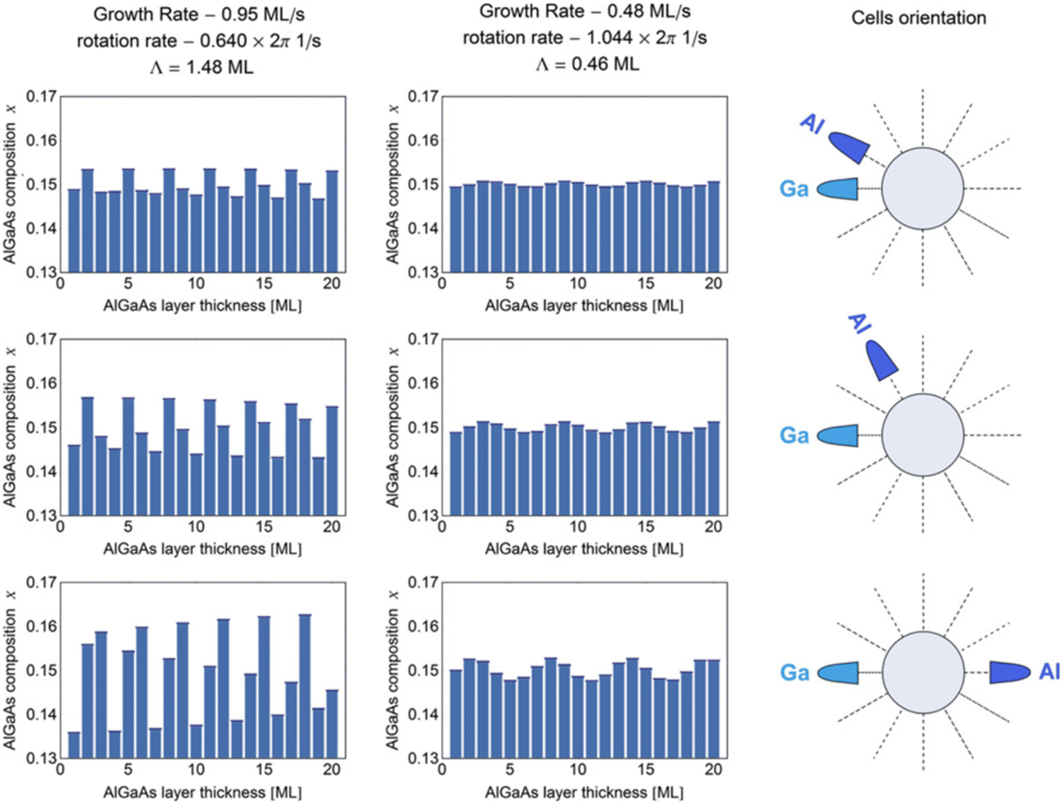 | ||
| Fig. 3 Illustration of using a properly designed substrate rotation speed to minimize the effect of non-optimized source configuration for compositionally uniform AlGaAs thin layers.67 | ||
These findings highlight the critical role of the source configuration on the growth kinetics, as well as how to mitigate the nonuniformities (e.g., thickness, composition) using a proper substrate rotation speed. On a separate note, the substrate rotation speed has also been found to affect the formation of ultrathin GaN quantum disks in nanowires.77
Lastly, it is noted that the angle between the axial direction of the source and the normal direction of the substrate needs to be optimized, in order to reduce the thickness variation maximally when rotating the substrate. This angle is typical in the range of 30 to 45 degrees, depending on the detailed system design and varying across different manufacturers.71,78 It is further noted that, while the state of the art thickness variation is around 0.5% or less (from wafer centre to wafer edge) on a 3′′ wafer, the typical thickness variation could be around 3%,67 due to the complexity in the system design (and thus the flux uniformity is sometimes compromised).
3. Uniqueness of nanowires
Different from the epitaxy of thin layers wherein only a horizontal surface is involved, the epitaxy of nanowires generally involves an additional surface – the sidewall (a vertical surface). This unique geometry of nanowires, coupled with different source configurations, can drastically affect the growth kinetics and consequently the material properties and device characteristics.In this section, I will discuss the MBE growth of GaN nanowires as an example. The geometric model for the MBE growth of GaN nanowires is described first, followed by the effect of the source configuration on the GaN nanowire morphology.
3.1. The geometric model
Over the past decade, quite elegant understanding has been developed with respect to the MBE growth of GaN nanowires. It is generally agreed that the anisotropy of surface energies, together with a geometric model, largely drives the nanowire vertical growth.68,70,71,79,80 Moreover, the anisotropy of surface energies, coupled with local III/N ratio variations (could be induced by nanowire geometry, nanowire density, source configurations, substrate rotation, or other factors), can mostly explain the formation of various crystalline planes/different nanowire facets and nanowire morphologies.66,81,82Fig. 4 shows the schematic of the geometric model, wherein α and β denote the flux incident angles for Ga and N, respectively. A simple geometric argument indicates that the ratio of the vertical growth rate to the lateral growth rate is π/tan(α) when the substrate is rotated during the growth.71 Namely, with a given incident angle of the N flux, a smaller α leads to a higher vertical growth rate to lateral growth rate ratio. This can be explained phenomenologically by the spread-out of the Ga adatoms (due to the substrate rotation) on the larger-area sidewall compared to the top surface, which tends to cause a higher growth rate vertically than laterally. This also implies that whether the substrate rotates or not makes a big difference on the nanowire morphology. Note that the growth rate difference here does not require any Ga or N diffusion.
 | ||
| Fig. 4 Illustration of the geometric model for the MBE growth of GaN nanowires. | ||
Furthermore, due to the unique nanowire sidewall (in contrast to the planar structure wherein there is no such sidewall), the Ga adatoms can diffusion along the sidewall, which may further modify the growth kinetics. For example, the diffusion may enhance the vertical growth and suppress the lateral growth. Moreover, for a given point on the sidewall, as the substrate rotates, Ga and N may not arrive at the same time, as such, the growth on the sidewall may mimic the metal-modulated epitaxy (MME),71,83 being a possible reason that the nanowire sidewall is typically highly smooth.
3.2. Source configuration
Galopin et al. have compared the MBE growth of GaN nanowires using a head-on N source (i.e., β = 0 in Fig. 4) and a directional N source (i.e., β ≠ 0 in Fig. 4).70 It is found that for the case of using the head-on N source, highly vertically aligned nanowires are formed, and the nanowires are not inversely tapered. In contrast, when the directional N source is used, the nanowires are noticeably inversely tapered. This, first of all, indicates a difference on the lateral growth and can be explained by that, for the head-on N source, the N/Ga ratio is high on the top surface but low on the sidewall, leading to almost no lateral growth. In addition, the diffused Ga adatoms from the sidewall can also contribute to the vertical growth. In contrast, for the directional N source, the N/Ga ratio on the top surface is significantly reduced, whereas the N/Ga ratio on the sidewall is increased. This reduces the vertical growth and enhances the lateral growth. Moreover, the higher N/Ga ratio on the sidewall also reduces the Ga desorption/diffusion along the sidewall, further enhancing the lateral growth. Secondly, the fact that the nanowires are tapered when a directional N source is used indicates a nonuniform lateral growth rate along the nanowire (from the nanowire bottom to the nanowire top).Treeck et al. have further studied the growth of a GaN shell using MBE on a GaN nanowire template.68 Experimentally, they have observed an enhanced shell formation in the nanowire top region and bottom region when there is no substrate rotation, and with the substrate rotation, an improved shell uniformity is obtained, as shown in Fig. 5(a). They have further investigated theoretically what if one changes the in-plane angle (β) between Ga and N while keeping the incident angle of N flux (α) the same (Fig. 5(b)) under different III/N ratios and substrate rotation speeds. It is found that the proximity of N to Ga enhances the shell uniformity, and high substrate rotation speeds and III/N ratios mimic increasing the proximity of N to Ga. These observations (both experimentally and theoretically) can be explained by the surface diffused Ga adatoms along the nanowire sidewall. Note that the enhanced shell formation in both the nanowire bottom and top regions could only be observed with low nanowire densities; for high nanowire densities, the shadow effect may suppress the formation of such shells.
 | ||
| Fig. 5 (a) SEM images of GaN nanowires with a regrown GaN shell with and without substrate rotation. (b) The model used to explain the GaN shell formation. Modification with permission from ref. 68. | ||
4. AlGaN nanowires by MBE
Compared to binary compound semiconductors, the epitaxial kinetics of ternary compound semiconductors is more complicated. As an example, for AlGaN ternary compounds, the incorporation of Ga could be determined by the presence of Al, due to the much stronger Al–N bond compared to the Ga–N bond.84 The difference in the bonding strength, together other factors such as surface features, will also affect the adatom diffusion kinetics along the nanowire sidewall during the MBE growth of AlGaN nanowires, leading to rich nanostructures such as AlGaN nanoclusters and Al-rich AlGaN shells. These features have been reviewed and discussed in depth previously, e.g., ref. 85–88. In this section, I will discussion the recent studies on how this difference, coupled with different chamber configurations, affects the properties of AlGaN nanowires.4.1. Effect of different Al sources
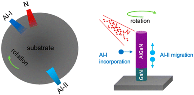 | ||
| Fig. 6 Illustration of different Al adatom kinetics at the growth front when Al sources in two different locations are used.89 | ||
The difference in the lateral growth at the growth front may cause a drastic difference in the Ga incorporation and thus the properties of AlGaN nanowires. Note that at typical growth temperatures for AlGaN nanowires, Ga is highly desorbing. However, in the case when Al-I is used, the enhanced lateral growth will reduce the gaps amongst the nanowires at the growth front, which may in consequence suppress the Ga desorption from the nanowire sidewall and thus favour Ga incorporation; this is illustrated in Fig. 7. In contrast, when Al-II is used, the undermined lateral growth will increase the gaps amongst nanowires, which may in turn favour the Ga desorption from the nanowire sidewall at the growth front.
 | ||
| Fig. 7 Illustration of different Ga adatom kinetics at the growth front in the epitaxy of AlGaN nanowires, induced by Al sources in two different locations. Different colours within the nanowire denote different device layers.85 The details are described in the main text when devices are discussed in section 4.1.4. The focus here is to illustrate Ga incorporation kinetics. | ||
The difference in the lateral growth at the growth front may also cause different nanowire uniformities. Higher lateral growth rates may lead to more uniform nanowires, due to the possibly undermined diffusion of highly mobile adatoms on the nanowire sidewall. Lastly, it is important to note that the discussions here are on bulk AlGaN nanowires rather than AlGaN quantum wells or quantum disks in nanowires.
 | ||
| Fig. 8 SEM images of different AlGaN nanowire samples using different Al sources.89 The insets are SEM images at higher magnifications. (a) Sample A is with Al-I. (b) Sample B is with Al-II. The difference between sample A and sample B is whether Al-I or Al-II is used. (c) Sample C is with Al-II but with optimized growth conditions. The details are explained in the main text. (d) Sample D is with Al-I. The difference between sample C and sample D is whether Al-I or Al-II is used. | ||
 | ||
| Fig. 9 (a) RTPL of different bulk AlGaN nanowire samples (i.e., without any quantum wells or quantum disks) using different Al sources. Samples A, B, C, and D are the same samples as shown in Fig. 8 for SEM studies. The black dot/dash curves are deconvoluted PL peaks. The details on the PL experiments can be found in ref. 89. (b) RT EL of AlGaN nanowire LEDs, correlating to the schematic shown in Fig. 7, using the two different Al sources. The measurement details can be found in ref. 85. The LED identification (i.e., LED B, LED C) from the original study is used. There are no correlations between LED B and sample B and between LED C and sample C. | ||
On the other hand, recent years have witnessed a growing interest of using nanowires as dislocation density filters to obtain compact epilayers and devices, e.g., ref. 93–98. The analysis here could provide insight on the chamber layout to enhance the nanowire coalescence.
In addition, the analysis here could also shed new light on explaining some features related to nanowires, such as compositional fluctuations in AlGaN nanowires,86,87 compositional nonuniformities in InGaN nanowires,99–101 and so on.
4.2. Substrate rotation
Fig. 10(a) shows the AlGaN p–i–n homojunction nanowire UV LED structure used to investigate the effect of the substrate rotation speed on the device characteristics. The thicknesses for n-GaN, n-AlGaN, i-AlGaN, p-AlGaN, p-GaN layers are around 100 nm, 40 nm, 40 nm, 40 nm, and 3 nm, respectively. Fig. 10(b) and (c) show the SEM images of the LED structures grown at 4 rpm and 15 rpm, respectively. It is seen that for the structure grown at 15 rpm, the nanowire uniformity is noticeably better, which can be explained by the geometric model described earlier. The detailed nanowire statistics can be found in ref. 102. | ||
| Fig. 10 (a) Schematic of the AlGaN nanowire UV LED structure used to investigate the substrate rotation speed. The insets are SEM images at higher magnifications. (b) and (c) SEM images of AlGaN nanowire LED structures grown at 4 rpm and 15 rpm, respectively. (d) and (e) The comparison of device characteristics. Details are described in the main text.102 | ||
Fig. 10(d) shows the comparison of the I–V characteristics between the two types of AlGaN nanowire UV LEDs. It is seen that using 15 rpm can noticeably improve the forward current of the device. In the meantime, using 15 rpm can also improve the light output power, thanks to the improved nanowire uniformity at the higher substrate rotation speed.102
It has been shown earlier that for the epilayer growth of III–V materials, to minimize the adverse effect of the directional sources, as well as to “bypass” the effect of different source configurations, high and carefully chosen substrate rotation speed is necessary. It is further shown earlier that high rotation speed leads to a uniform GaN shell. Discussions in this section also indicate that high rotation speed improves the AlGaN nanowire uniformity and consequently the device performance. Therefore, it might be seen that, using high substrate rotation speed might always be favourable to mitigate non-ideal chamber configurations.
5. Concluding remarks
In summary, the recent advancement on the MBE grown AlGaN nanowires, which are an emerging material platform for UV photonics, as well as high-power and RF electronics, is discussed in this minireview. Compared to epilayers wherein only a horizontal surface is involved, the growth of nanowires is more complicated, due to the presence of an additional surface, i.e., the sidewall of nanowires. This is further complicated by different source configurations, as well as different bonding strengths in ternary compound semiconductors. As such, the focus of this minireview is on the chamber configuration dependent material properties and device characteristics. Given the complexity of the ultrahigh vacuum (UHV) systems, it might be nearly impossible for one to vent the UHV growth chamber only for the source configuration dependent material properties and device characteristics investigation purpose. I hope this minireview can provide some useful insight for the material and device development using AlGaN nanowires and other semiconductor nanowires beyond AlGaN.Data availability
Data is available upon reasonable request to the author.Author contributions
This article is written by S. Z. without using any artificial intelligence (AI) tools.Conflicts of interest
There are no conflicts to declare.Acknowledgements
This work is supported by Natural Sciences and Engineering Research Council of Canada, Fonds de recherche du Québec – Nature et technologies, and McGill University.Notes and references
- Y. Liang, C. Li, Y. Z. Huang and Q. Zhang, ACS Nano, 2020, 14, 14375–14390 CrossRef CAS PubMed.
- J. Meng and Z. Li, Adv. Mater., 2020, 32, e2000130 CrossRef PubMed.
- T. A. Pham, A. Qamar, T. Dinh, M. K. Masud, M. Rais-Zadeh, D. G. Senesky, Y. Yamauchi, N. T. Nguyen and H. P. Phan, Adv. Sci., 2020, 7, 2001294 Search PubMed.
- X. Chen, B. Chen, B. Jiang, T. Gao, G. Shang, S. T. Han, C. C. Kuo, V. A. L. Roy and Y. Zhou, Adv. Funct. Mater., 2022, 33, 2208807 CrossRef.
- Z. Li, Z. He, C. Xi, F. Zhang, L. Huang, Y. Yu, H. H. Tan, C. Jagadish and L. Fu, Adv. Mater. Technol., 2023, 8, 2202126 CrossRef CAS.
- S. Steinhauer, S. Gyger and V. Zwiller, Appl. Phys. Lett., 2021, 118, 100501 Search PubMed.
- K. Ren, C. Li, Z. Fang and F. Feng, Laser Photonics Rev., 2023, 17, 2200758 CrossRef.
- W. Cao, H. Bu, M. Vinet, M. Cao, S. Takagi, S. Hwang, T. Ghani and K. Banerjee, Nature, 2023, 620, 501–515 CrossRef CAS PubMed.
- K. Peng, D. Jevtics, F. Zhang, S. Sterzl, D. A. Damry, M. U. Rothmann, B. Guilhabert, M. J. Strain, H. H. Tan, L. M. Herz, L. Fu, M. D. Dawson, A. Hurtado, C. Jagadish and M. B. Johnston, Science, 2020, 368, 510 Search PubMed.
- S. Zhao, in Semiconductors and Semimetals, ed. Z. Mi and H. H. Tan, ScienceDirect, 2024, vol. 116, p. 1 Search PubMed.
- F. Glas, Phys. Rev. B: Condens. Matter Mater. Phys., 2006, 74, r121302 CrossRef.
- J. Y. Tsao, M. H. Crawford, M. E. Coltrin, A. J. Fischer, D. D. Koleske, G. S. Subramania, G. T. Wang, J. J. Wierer and R. F. Karlicek, Adv. Opt. Mater., 2014, 2, 809–836 CrossRef CAS.
- J. Y. Tsao, S. Chowdhury, M. A. Hollis, D. Jena, N. M. Johnson, K. A. Jones, R. J. Kaplar, S. Rajan, C. G. Van de Walle, E. Bellotti, C. L. Chua, R. Collazo, M. E. Coltrin, J. A. Cooper, K. R. Evans, S. Graham, T. A. Grotjohn, E. R. Heller, M. Higashiwaki, M. S. Islam, P. W. Juodawlkis, M. A. Khan, A. D. Koehler, J. H. Leach, U. K. Mishra, R. J. Nemanich, R. C. N. Pilawa-Podgurski, J. B. Shealy, Z. Sitar, M. J. Tadjer, A. F. Witulski, M. Wraback and J. A. Simmons, Adv. Electron. Mater., 2018, 4, 1600501 CrossRef.
- D. Iida and K. Ohkawa, Semicond. Sci. Technol., 2022, 37, 013001 CrossRef CAS.
- M. S. Wong, J. S. Speck, S. Nakamura and S. P. DenBaars, IEEE J. Quantum Electron., 2022, 58, 1–11 Search PubMed.
- W. Y. Fu and H. W. Choi, J. Appl. Phys., 2022, 132, 060903 CAS.
- J. Y. Lin and H. X. Jiang, Appl. Phys. Lett., 2020, 116, 100502 CAS.
- H. Amano, R. Collazo, C. D. Santi, S. Einfeldt, M. Funato, J. Glaab, S. Hagedorn, A. Hirano, H. Hirayama, R. Ishii, Y. Kashima, Y. Kawakami, R. Kirste, M. Kneissl, R. Martin, F. Mehnke, M. Meneghini, A. Ougazzaden, P. J. Parbrook, S. Rajan, P. Reddy, F. Römer, J. Ruschel, B. Sarkar, F. Scholz, L. J. Schowalter, P. Shields, Z. Sitar, L. Sulmoni, T. Wang, T. Wernicke, M. Weyers, B. Witzigmann, Y.-R. Wu, T. Wunderer and Y. Zhang, J. Phys. D: Appl. Phys., 2020, 53, 503001 CAS.
- H. Amano, Y. Baines, E. Beam, M. Borga, T. Bouchet, P. R. Chalker, M. Charles, K. J. Chen, N. Chowdhury, R. Chu, C. De Santi, M. M. De Souza, S. Decoutere, L. Di Cioccio, B. Eckardt, T. Egawa, P. Fay, J. J. Freedsman, L. Guido, O. Häberlen, G. Haynes, T. Heckel, D. Hemakumara, P. Houston, J. Hu, M. Hua, Q. Huang, A. Huang, S. Jiang, H. Kawai, D. Kinzer, M. Kuball, A. Kumar, K. B. Lee, X. Li, D. Marcon, M. März, R. McCarthy, G. Meneghesso, M. Meneghini, E. Morvan, A. Nakajima, E. M. S. Narayanan, S. Oliver, T. Palacios, D. Piedra, M. Plissonnier, R. Reddy, M. Sun, I. Thayne, A. Torres, N. Trivellin, V. Unni, M. J. Uren, M. Van Hove, D. J. Wallis, J. Wang, J. Xie, S. Yagi, S. Yang, C. Youtsey, R. Yu, E. Zanoni, S. Zeltner and Y. Zhang, J. Phys. D: Appl. Phys., 2018, 51, 163001 Search PubMed.
- C.-C. Lin, Y.-R. Wu, H.-C. Kuo, M. S. Wong, S. P. DenBaars, S. Nakamura, A. Pandey, Z. Mi, P. Tian, K. Ohkawa, D. Iida, T. Wang, Y. Cai, J. Bai, Z. Yang, Y. Qian, S.-T. Wu, J. Han, C. Chen, Z. Liu, B.-R. Hyun, J.-H. Kim, B. Jang, H.-D. Kim, H.-J. Lee, Y.-T. Liu, Y.-H. Lai, Y.-L. Li, W. Meng, H. Shen, B. Liu, X. Wang, K.-L. Liang, C.-J. Luo and Y.-H. Fang, JPhys Photonics, 2023, 5, 042502 Search PubMed.
- A. Pandey, M. Reddeppa and Z. Mi, Light: Adv. Manuf., 2023, 4, 31 Search PubMed.
- Z. Li, Y. Liu, F. Feng, Z. Liu, M. Wong, H. S. Kwok and Z. Liu, IEEE Open J. Immersive Disp., 2024, 1, 62 Search PubMed.
- K. Behrman and I. Kymissis, Nat. Electron., 2022, 5, 564–573 CrossRef.
- T. Takano, T. Mino, J. Sakai, N. Noguchi, K. Tsubaki and H. Hirayama, Appl. Phys. Express, 2017, 10, 031002 CrossRef.
- Z. Zhang, M. Kushimoto, T. Sakai, N. Sugiyama, L. J. Schowalter, C. Sasaoka and H. Amano, Appl. Phys. Express, 2019, 12, 124003 CAS.
- M. Kneissl, T.-Y. Seong, J. Han and H. Amano, Nat. Photonics, 2019, 13, 233–244 Search PubMed.
- D. Li, K. Jiang, X. Sun and C. Guo, Adv. Opt. Photonics, 2018, 10, 43 Search PubMed.
- T. D. Moustakas and R. Paiella, Rep. Prog. Phys., 2017, 80, 106501 Search PubMed.
- Q. Zhang, X. Yin and S. Zhao, Phys. Status Solidi RRL, 2021, 15, 2100090 CAS.
- S. Zhao and Z. Mi, Crystals, 2017, 7, 268 Search PubMed.
- S. Zhao, H. P. T. Nguyen, M. G. Kibria and Z. Mi, Prog. Quantum Electron., 2015, 44, 14–68 Search PubMed.
- S. Zhao and Z. Mi, IEEE J. Quantum Electron., 2018, 54, 1–9 Search PubMed.
- M. Spies and E. Monroy, Semicond. Sci. Technol., 2019, 34, 053002 CrossRef CAS.
- F. Chen, X. Ji and S. P. Lau, Mater. Sci. Eng., R, 2020, 142, 100578 CrossRef.
- V. Vignesh, Y. Wu, S.-U. Kim, J.-K. Oh, C. Bagavath, D.-Y. Um, Z. Mi and Y.-H. Ra, J. Inf. Disp., 2023, 25, 13–59 Search PubMed.
- S. Zhao, J. Lu, X. Hai and X. Yin, Micromachines, 2020, 11, 125 Search PubMed.
- J. Bosch, C. Durand, B. Alloing and M. Tchernycheva, J. Inf. Disp., 2024, 25, 61–73 Search PubMed.
- Y. Wu, X. Liu, A. Pandey, P. Zhou, W. J. Dong, P. Wang, J. Min, P. Deotare, M. Kira, E. Kioupakis and Z. Mi, Prog. Quantum Electron., 2022, 85, 100401 CrossRef.
- S. Zhao, A. T. Connie, M. H. Dastjerdi, X. H. Kong, Q. Wang, M. Djavid, S. Sadaf, X. D. Liu, I. Shih, H. Guo and Z. Mi, Sci. Rep., 2015, 5, 8332 CrossRef CAS.
- M. J. Holmes, K. Choi, S. Kako, M. Arita and Y. Arakawa, Nano Lett., 2014, 14, 982–986 CrossRef CAS PubMed.
- Y.-H. Ra and C.-R. Lee, Nano Energy, 2021, 84, 105870 CrossRef CAS.
- Y.-H. Ra, R. T. Rashid, X. Liu, S. M. Sadaf, K. Mashooq and Z. Mi, Sci. Adv., 2020, 6, eaav7523 CrossRef CAS.
- M. F. Vafadar and S. Zhao, Sci. Rep., 2023, 13, 6633 CrossRef CAS.
- M. F. Vafadar and S. Zhao, ACS Nano, 2024, 18, 14290–14297 CrossRef CAS.
- S. Zhao, X. Liu, Y. Wu and Z. Mi, Appl. Phys. Lett., 2016, 109, 191106 CrossRef.
- S. Zhao, X. Liu, S. Y. Woo, J. Kang, G. A. Botton and Z. Mi, Appl. Phys. Lett., 2015, 107, 043101 CrossRef.
- M. Fathabadi and S. Zhao, ACS Photonics, 2023, 10, 2825–2831 CrossRef CAS.
- M. Fathabadi and S. Zhao, ACS Photonics, 2023, 10, 1969–1975 CrossRef CAS.
- M. Fathabadi, Y. Yin, S. Li and S. Zhao, Adv. Opt. Mater., 2023, 12, 2302372 CrossRef.
- Y. Luo, D. Wang, Y. Kang, X. Liu, S. Fang, M. H. Memon, H. Yu, H. Zhang, D. Luo, X. Sun, B. S. Ooi, C. Gong, Z. Xu and H. Sun, Adv. Opt. Mater., 2022, 10, 2102839 CrossRef CAS.
- M. G. Kibria, F. A. Chowdhury, S. Zhao, B. AlOtaibi, M. L. Trudeau, H. Guo and Z. Mi, Nat. Commun., 2015, 6, 6797 CrossRef CAS PubMed.
- M. G. Kibria, S. Zhao, F. A. Chowdhury, Q. Wang, H. P. T. Nguyen, M. L. Trudeau, H. Guo and Z. Mi, Nat. Commun., 2014, 5, 3825 CrossRef CAS.
- P. Zhou, I. A. Navid, Y. Ma, Y. Xiao, P. Wang, Z. Ye, B. Zhou, K. Sun and Z. Mi, Nature, 2023, 613, 66–70 CrossRef CAS PubMed.
- M. Henini, Molecular Beam Epitaxy - From Research to Mass Production, Elsevier, 1st edn, 2012 Search PubMed.
- J. Orton and T. Foxon, Molecular beam epitaxy - a short history, Oxford University Press, 2015 Search PubMed.
- M. Henini, Molecular Beam Epitaxy - From Research to Mass Production, Elsevier, 2nd edn, 2018 Search PubMed.
- M. A. Herman, W. Richter and H. Sitter, Epitaxy: physical principles and technical implementation, Springer Science & Business Media, 2013 Search PubMed.
- L. L. Chang and K. Ploog, Molecular beam epitaxy and heterostructures, Springer Science & Business Media, 2012 Search PubMed.
- K. A. Bertness, A. W. Sanders, D. M. Rourke, T. E. Harvey, A. Roshko, J. B. Schlager and N. A. Sanford, Adv. Funct. Mater., 2010, 20, 2911–2915 CrossRef CAS.
- A. Bengoechea-Encabo, F. Barbagini, S. Fernandez-Garrido, J. Grandal, J. Ristic, M. A. Sanchez-Garcia, E. Calleja, U. Jahn, E. Luna and A. Trampert, J. Cryst. Growth, 2011, 325, 89–92 CrossRef CAS.
- K. Kishino, H. Sekiguchi and A. Kikuchi, J. Cryst. Growth, 2009, 311, 2063–2068 CrossRef CAS.
- K. Yamano, K. Kishino, H. Sekiguchi, T. Oto, A. Wakahara and Y. Kawakami, J. Cryst. Growth, 2015, 425, 316–321 CrossRef CAS.
- R. Wang, Y. H. Ra, Y. Wu, S. Zhao, H. P. T. Nguyen, I. Shih and Z. Mi, Proc. SPIE, 2016, 9748, 9748IS Search PubMed.
- Y.-H. Ra, R. T. Rashid, X. Liu, J. Lee and Z. Mi, Adv. Funct. Mater., 2017, 27, 1702364 CrossRef.
- M. F. Vafadar and S. Zhao, ACS Appl. Nano Mater., 2022, 5, 16045–16050 CrossRef CAS.
- F. Pantle, M. Karlinger, S. Wörle, F. Becker, T. Höldrich, E. Sirotti, M. Kraut and M. Stutzmann, J. Appl. Phys., 2022, 132, 184304 CrossRef CAS.
- Z. R. Wasilewski, in Molecular Beam Epitaxy - From Research to Mass Production, ed. M. Henini, Elsevier, 1st edn, 2012, ch. 28 Search PubMed.
- D. van Treeck, S. Fernández-Garrido and L. Geelhaar, Phys. Rev. Mater., 2020, 4, 013404 CrossRef CAS.
- N. V. Sibirev, M. Tchernycheva, M. A. Timofeeva, J.-C. Harmand, G. E. Cirlin and V. G. Dubrovskii, J. Appl. Phys., 2012, 111, 104317 CrossRef.
- E. Galopin, L. Largeau, G. Patriarche, L. Travers, F. Glas and J. C. Harmand, Nanotechnology, 2011, 22, 245606 Search PubMed.
- C. T. Foxon, S. V. Novikov, J. L. Hall, R. P. Campion, D. Cherns, I. Griffiths and S. Khongphetsak, J. Cryst. Growth, 2009, 311, 3423–3427 Search PubMed.
- F. Glas, Phys. Status Solidi B, 2010, 247, 254–258 Search PubMed.
- A. Khalatpour, A. K. Paulsen, C. Deimert, Z. R. Wasilewski and Q. Hu, Nat. Photonics, 2020, 15, 16–20 CrossRef.
- S. Fujikawa, T. Ishiguro, K. Wang, W. Terashima, H. Fujishiro and H. Hirayama, J. Cryst. Growth, 2019, 510, 47–49 CrossRef CAS.
- H. Hirayama, W. Terashima, S. Toyoda and N. Kamata, presented in part at the 74th Annual Device Research Conference (DRC), 2016 Search PubMed.
- S. Fathololoumi, E. Dupont, C. W. I. Chan, Z. R. Wasilewski, S. R. Laframboise, D. Ban, A. Matyas, C. Jirauschek, Q. Hu and H. C. Liu, Opt. Express, 2012, 20, 3866 Search PubMed.
- A. T. Sarwar, B. J. May, M. F. Chisholm, G. J. Duscher and R. C. Myers, Nanoscale, 2016, 8, 8024–8032 Search PubMed.
- Z. R. Wasilewski, G. C. Aers, A. J. SpringThorpe and C. J. Miner, J. Vac. Sci. Technol., B: Microelectron. Nanometer Struct.--Process., Meas., Phenom., 1991, 9, 120–131 Search PubMed.
- K. A. Bertness, N. A. Sanford and A. V. Davydov, IEEE J. Sel. Top. Quantum Electron., 2011, 17, 847 CAS.
- V. Consonni, Phys. Status Solidi RRL, 2013, 7, 699–712 CAS.
- H. Li, L. Geelhaar, H. Riechert and C. Draxl, Phys. Rev. Lett., 2015, 115, 085503 CrossRef PubMed.
- V. Consonni, M. Knelangen, L. Geelhaar, A. Trampert and H. Riechert, Phys. Rev. B: Condens. Matter Mater. Phys., 2010, 81, 085310 Search PubMed.
- B. Gunning, J. Lowder, M. Moseley and W. Alan Doolittle, Appl. Phys. Lett., 2012, 101, 082106 CrossRef.
- E. Iliopoulos and T. D. Moustakas, Appl. Phys. Lett., 2002, 81, 295 CAS.
- Q. Zhang, H. Yuan, M. F. Vafadar, G. A. Botton and S. Zhao, Cryst. Growth Des., 2024, 24, 5263–5268 CrossRef CAS.
- S. Zhao, S. Y. Woo, M. Bugnet, X. Liu, J. Kang, G. A. Botton and Z. Mi, Nano Lett., 2015, 15, 7801–7807 CrossRef CAS PubMed.
- M. Belloeil, B. Gayral and B. Daudin, Nano Lett., 2016, 16, 960–966 CrossRef CAS PubMed.
- K. Hestroffer and B. Daudin, J. Appl. Phys., 2013, 114, 244305 CrossRef.
- M. F. Vafadar, Q. Zhang and S. Zhao, Cryst. Growth Des., 2023, 23, 3091–3097 CrossRef CAS.
- Y. Taniyasu, M. Kasu and T. Makimoto, Nature, 2006, 441, 325–328 CAS.
- S. Zhao, M. Djavid and Z. Mi, Nano Lett., 2015, 15, 7006 CAS.
- S. Zhao, S. Y. Woo, S. M. Sadaf, Y. Wu, A. Pofelski, D. A. Laleyan, R. T. Rashid, Y. Wang, G. A. Botton and Z. Mi, APL Mater., 2016, 4, 086115 Search PubMed.
- Q. Li, Y. Lin, J. R. Creighton, J. J. Figiel and G. T. Wang, Adv. Mater., 2009, 21, 2416–2420 CAS.
- A. Zhong and K. Hane, Nanoscale Res. Lett., 2012, 7, 686 Search PubMed.
- X. Yin, Q. Zhang and S. Zhao, Cryst. Growth Des., 2021, 21, 3645 CAS.
- Q. Zhang, H. Parimoo, E. Martel and S. Zhao, Sci. Rep., 2022, 12, 7230 CAS.
- Y. Wu, Y. Wang, K. Sun, A. Aiello, P. Bhattacharya and Z. Mi, J. Cryst. Growth, 2018, 498, 109–114 CAS.
- B. J. May, E. C. Hettiaratchy, B. Wang, C. M. Selcu, B. D. Esser, D. W. McComb and R. C. Myers, Phys. Status Solidi RRL, 2024, 18, 2300399 CAS.
- F. Limbach, C. Hauswald, J. Lahnemann, M. Wolz, O. Brandt, A. Trampert, M. Hanke, U. Jahn, R. Calarco, L. Geelhaar and H. Riechert, Nanotechnology, 2012, 23, 465301 Search PubMed.
- A. L. Bavencove, G. Tourbot, J. Garcia, Y. Desieres, P. Gilet, F. Levy, B. Andre, B. Gayral, B. Daudin and L. S. Dang, Nanotechnology, 2011, 22, 345705 CrossRef CAS PubMed.
- W. Y. Fu and H. W. Choi, Phys. Status Solidi RRL, 2022, 16, 2100628 CrossRef CAS.
- M. F. Vafadar, R. B. Arif, Q. Zhang and S. Zhao, J. Vac. Sci. Technol., B: Nanotechnol. Microelectron.: Mater., Process., Meas., Phenom., 2023, 41, 030601 CAS.
| This journal is © The Royal Society of Chemistry 2025 |