
 Open Access Article
 This Open Access Article is licensed under a Creative Commons Attribution-Non Commercial 3.0 Unported Licence
Improved optical quality of heteroepitaxially grown metal–organic framework thin films by modulating the crystal growth†
Yuka
Koseki
a,
Kenji
Okada
 *a,
Shotaro
Hashimoto
b,
Shun
Hirouchi
b,
Arisa
Fukatsu
a and
Masahide
Takahashi
*a
*a,
Shotaro
Hashimoto
b,
Shun
Hirouchi
b,
Arisa
Fukatsu
a and
Masahide
Takahashi
*a
aDepartment of Materials Science, Graduate School of Engineering, Osaka Metropolitan University, Sakai, Osaka 599-8531, Japan. E-mail: k_okada@omu.ac.jp; masa@omu.ac.jp; Fax: +81 72 254 9309; Tel: +81 72 254 9748
bDepartment of Materials Science, Graduate School of Engineering, Osaka Prefecture University, Sakai, Osaka 599-8531, Japan
First published on 20th June 2024
Abstract
Fabricating high-quality thin films of metal–organic frameworks (MOFs) is important for integrating MOFs in various applications. Specifically, optical/electrical devices require MOF thin films that are crystallographically oriented, with closely packed crystals and smooth surfaces. Although the heteroepitaxial growth approach of MOFs on metal hydroxides has been demonstrated to control the orientation of the three crystallographic axes, the fabrication of MOF thin films with both three-dimensional crystallographic orientation and smooth surfaces remains a challenge. In this study, we report the fabrication of high-quality thin films of MOFs with closely packed MOF crystals, smooth surfaces, optical transparency, and crystal alignment by modulating the crystal growth of MOFs using the heteroepitaxial growth approach. High-quality thin films of Cu-paddlewheel-based pillar-layered MOFs are fabricated on oriented Cu(OH)2 thin films via epitaxial growth using acetate ions as modulators to control the crystal morphology. Increasing the modulator concentration results in a uniform crystal shape with a relatively long one-dimensional pore direction and uniform heterogeneous nucleation over the entire film. The MOF thin films fabricated using the modulator exhibit high optical transparency. High-quality MOF thin films with dense and flat surfaces will pave the way for integrating MOFs into sophisticated optical and electrical devices.
 Kenji Okada | Associate Professor Kenji Okada received his Ph. D (Engineering) in Material Science from Osaka Prefecture University in 2014. After receiving the degree, he worked as a JSPS (Japan Society for the Promotion of Science) postdoctoral researcher from 2014 to 2015. From 2015 to 2017, he was appointed as an assistant professor at Osaka University. He moved to Osaka Metropolitan University (former: Osaka Prefecture University) as an assistant professor in 2017 and was promoted to Associate Professor in 2020. He was chosen as ‘Leading Initiative for Excellent Young Researchers (LEADER)’ by MEXT in 2017. He has also worked as a PRESTO researcher of JST from 2019 to 2023. His research interest is to fabricate nanomaterials (e.g., 1D metal hydroxide, metal organic frameworks, mesoporous silica) with macroscopically controlled orientation and aggregation for electrical, optical and thermal applications. As also selected as a one of J. Mater. Chem. A Emerging Investigators in 2021, he is recognized as one of rising stars of materials chemistry, nanoscience and nanotechnology researches. |
Introduction
Metal–organic frameworks (MOFs), also called porous coordination polymers (PCPs), are crystalline porous materials made from the assembly of metal ions and organic linkers.1,2 Owing to their structural and chemical versatility, they can be utilised for gas separation,3 storage,4 and catalysis.5,6 Their high versatility and well-defined structures allow MOFs to be used in advanced optical or electrical devices.7–11 Although MOFs are typically obtained in powder forms, homogeneous MOF films are required for those applications.12,13 Therefore, it is necessary to develop a fabrication process for producing high-quality thin films of MOFs with high crystal orientations, smooth and homogeneous surfaces, and controlled thicknesses to integrate MOFs into advanced devices.14–16 Among the fabrication methods for MOF thin films, the layer-by-layer (LbL) approach17 has produced highly crystalline, oriented, and homogeneous MOF films with controlled thickness.13 For example, a continuous-flow LbL technique allows the fabrication of an MIL-68(In) film with excellent optical quality on a quartz crystal microbalance (QCM), which enables the integration of MOF films in optical cavity sensing.18 As demonstrated earlier, improving the quality of MOF thin films, particularly surface homogeneity, has resulted in using MOFs for advanced device applications. Another significant challenge for MOF-based device applications is controlling the alignment of MOF crystals in both the out-of-plane and in-plane directions to maximise device performance.13,19–22 Consequently, we developed a fabrication process for MOF thin films with both out-of-plane and in-plane orientations via the epitaxial growth of MOF crystals on preformed copper hydroxide substrates,23 which can be converted to MOFs in relatively short and mild reactions. Three-dimensional (3D)-oriented MOF films and multilayered MOF (MOF-on-MOF) thin films24,25 have demonstrated unique in-plane anisotropic optical26,27 and electrical28 properties on a macroscopic scale (measured in centimetres), owing to the macroscopic alignment of well-defined micropores and frameworks of MOFs, which could not be achieved by MOF films with only one-dimensional (1D) and out-of-plane orientations. For instance, a 3D-oriented film of Cu2(linker)2dabco (linker: 1,4-benzenedicarboxylate (bdc), 1,4-naphthalenedicarboxylate (1,4-ndc), dabco: 1,4-diazabicyclo[2.2.2]octane), which has 1D nanochannels along the pillar-connecting direction, showed in-plane anisotropic polarisation-dependent light absorption after the aligned inclusion of trans-azobenzene into the 1D nanochannels.26 Although we have demonstrated the simple fabrication of 3D-oriented MOF films that show unique optical and electrical properties, in some MOFs, particularly Cu2(bdc)2dabco, there is a lack of surface smoothness in the films owing to the overgrowth of crystals in particular crystal axes23,26 (see Fig. S1 and S2†). The Cu2(bdc)2dabco MOF consists of two-dimensional (2D) square lattices (containing Cu paddlewheel units) connected to dabco as a pillar. In the epitaxial growth of Cu2(bdc)2dabco on Cu(OH)2, preferential crystal growth in the coordination direction of bdc (lateral direction in 2D square lattices) and the non-uniform heterogeneous nucleation of MOF crystals on Cu(OH)2 resulted in the fabrication of oriented MOF films consisting of discrete MOF crystals and, correspondingly, opaque MOF-oriented films with rough surfaces. In this study, we report a fabrication method for oriented Cu-paddlewheel-based MOF thin films with closely packed MOF crystals, smooth surfaces, and high optical transparency by controlling the crystal morphology using a modulator that controls the direction of MOF crystal growth (Fig. 1). Modulators, also called capping reagents, have been used to control the size and morphology of MOF particles.29–31 Here, modulator-assisted control of the crystal morphology was applied for the first time to an epitaxial growth approach for Cu2(bdc)2dabco MOF on Cu(OH)2![[thin space (1/6-em)]](https://www.rsc.org/images/entities/char_2009.gif) 23,26 films. Preferential crystal growth in the coordination direction of bdc (a- and b-axis direction of Cu2(bdc)2dabco) is prevented by the modulator, resulting in a change in the crystal morphology, which is relatively long in the coordination direction of dabco (c-axis direction (1D channel direction) of Cu2(bdc)2dabco).
23,26 films. Preferential crystal growth in the coordination direction of bdc (a- and b-axis direction of Cu2(bdc)2dabco) is prevented by the modulator, resulting in a change in the crystal morphology, which is relatively long in the coordination direction of dabco (c-axis direction (1D channel direction) of Cu2(bdc)2dabco).
 | ||
| Fig. 1 The conceptual images of the present study (a) representing epitaxial growth of Cu2(bdc)2dabco on Cu(OH)2 without and with a modulator. (b) Without a modulator, MOF crystals preferentially grow in the direction of a 2D layer (a- and b-axis of Cu2(bdc)2dabco). (c) With a modulator, MOF crystals grow in the direction of 1D channels (c-axis of Cu2(bdc)2dabco). | ||
Furthermore, using a modulator led to uniform heterogeneous nucleation of MOF crystals on the Cu(OH)2 surface during the early stage of the reaction. Thus, out-of-plane/in-plane-oriented Cu2(bdc)2dabco thin films with closely packed MOF crystals and smooth surfaces were fabricated owing to controlled crystal growth and uniform heterogeneous nucleation. The obtained films with smooth surfaces showed improved optical quality due to the decrease of light scattering on the surface. These densely packed MOF thin films with flat surfaces will facilitate the integration of MOFs into advanced optical and electrical devices.
Methods
Materials
1,4-benzenedicarboxylic acid (H2bdc), acetic acid (99.7%), sodium acetate, methanol, and ethanol were purchased from FUJIFILM Wako Pure Chemical Corporation (Osaka, Japan). 1,4-Diazabicyclo[2.2.2]octane (dabco) and 2,6-naphthalenedicarboxylic acid (2,6-H2ndc) were purchased from Tokyo Chemical Industry Co., Ltd (Tokyo, Japan). All reactants were used without further purification.Synthesis of Cu2(bdc)2dabco-oriented thin films with a modulator
Cu(OH)2-oriented films on Si wafers (∼15 mm × 20 mm) or silica glass (∼20 mm × 20 mm) were fabricated according to our previous report.23 H2bdc (4 mM) and dabco (256 mM) were dissolved in methanol at 40 °C. Organic linker (bdc) and pillar (dabco) concentrations were optimized for epitaxial growth of Cu2(bdc)2dabco as the previous report.26 Diluted acetic acid (1742 mM) and sodium acetate were used as the modulators, and the molar ratio of acetic acid to sodium acetate was fixed at 9:1. The modulator was added to a methanol solution containing H2bdc and dabco at predefined concentrations of up to 50 mM and dissolved by sonication. Cu(OH)2-oriented films on Si wafers were immersed in 50 mL of the solution and left for an hour at 60 °C. Subsequently, the film was removed from the solution, washed with ethanol, and dried using an air gun. To fabricate the MOF films on silica glass, the reaction was conducted in 10 mL of the reaction solution in a Teflon container.
Characterisation
The obtained MOF films were identified by X-ray diffraction (Smart Lab, Rigaku Corporation, Japan) using CuKα radiation (λ = 0.154 nm). The degree of in-plane orientation of MOF crystals was estimated by azimuthal angle dependence of intensity profiles (ϕ scan) (Fig. S3†). The crystal morphologies of the obtained MOF films were investigated using field-emission scanning electron microscopy (FE-SEM; SU8010, Hitachi High-Tech Corporation, Japan) (with an electrically conducting Pt coating). The nucleation per unit area of the obtained MOF films was examined by counting the number of nuclei in 5 μm × 5 μm square of the films using SEM images. The thickness of the Cu2(bdc)2dabco-oriented films on the Si wafer was measured by investigating the average height of the films from the Si wafer at five different locations using a surface profilometer (Surfcorder ET200, Kosaka Laboratory Ltd, Japan). Cu2(bdc)2dabco nucleation was investigated using Fourier transform infrared spectroscopy (FT-IR; FT-IR-4600 spectrometer, JASCO, Japan). The surface roughness of the obtained MOF films was examined by analysing the average surface roughness (Sa: arithmetical mean height) of 5 μm × 5 μm square of the films for 3D images obtained by confocal laser scanning microscopy equipped with atomic force microscopy (CLSM, AFM: Nanosearch Microscope, SFT-3500S, Shimadzu Corporation, Japan). The haze spectra of the Cu2(bdc)2dabco films on silica glass were obtained by measuring the total transmittance and sample scattering rate using a UV-Vis spectrophotometer (V-670, JASCO, Japan) equipped with an integrating sphere.Results and discussion
Cu2(bdc)2dabco32,33 thin films were fabricated using the one-pot method, with acetic acid and sodium acetate as modulators. The crystal structure and crystallographic orientation along all three axes of the MOF films were evaluated using previously reported protocols23 and X-ray diffraction (XRD). For the Cu2(bdc)2dabco thin film synthesised without a modulator, the intense 0k0 reflections of Cu2(bdc)2dabco in the out-of-plane XRD measurement and the intense h00 and 00l reflections of the MOF in the two types of in-plane XRD measurements (parallel and perpendicular, respectively), which showed substantial X-ray incidence angular dependence, were confirmed, similar to our previous report23,26 (Fig. S3†). These results show the fabrication of oriented MOF films with out-of-plane and in-plane orientations, where the (0k0) lattice planes of the MOF were parallel to the substrate and the (h00) and (00l) lattice planes of the MOF were orthogonal to each other and perpendicular to the substrate wafer throughout the entire film (∼15 mm × 20 mm). The same crystallographic orientation was confirmed for all the films, regardless of whether the modulator was used (Fig. 2(a) and S4†). The heteroepitaxial relationship between Cu(OH)2 and Cu2(bdc)2dabco was confirmed using ϕ scan measurement; the a- and c-axis of Cu(OH)2 are parallel to the c- and a-axis of Cu2(bdc)2dabco, respectively, which is consistent with our previous results (Fig. S5†). The degree of in-plane orientation was >80% regardless of the use of the modulator, as confirmed by the azimuthal angle dependence of the intensity profiles (Fig. 2(b)). Based on the heteroepitaxial growth mechanism, the degree of orientation of the MOF thin films (∼80%) reflected that of the Cu(OH)2 thin films.23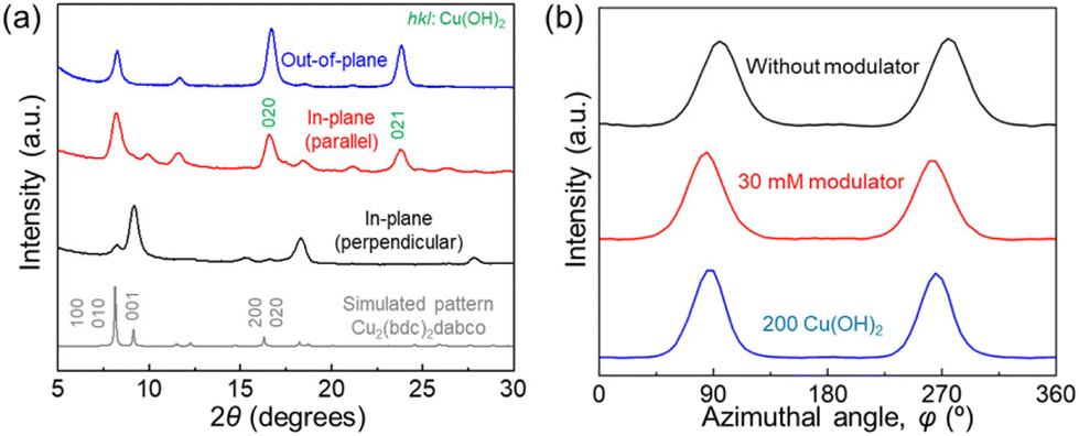 | ||
| Fig. 2 (a) XRD patterns of an oriented Cu2(bdc)2dabco thin film fabricated with a modulator (30 mM). (b) ϕ scan profiles for the (001) reflection of Cu2(bdc)2dabco in oriented Cu2(bdc)2dabco thin films fabricated without and with a modulator (30 mM) and (200) reflection of Cu(OH)2 in a Cu(OH)2-oriented film. | ||
The morphological changes in the MOF crystals owing to the effect of the modulator were investigated using an SEM. An SEM image of the oriented Cu2(bdc)2dabco thin film, synthesised without a modulator, showed that the size of the MOF particles along the a-axis (vertical direction) was longer than that along the c-axis (horizontal direction). The aspect ratio of the MOF crystals in the a-axis to the c-axis direction was ∼4.11 (Fig. 3(a)) due to the preferential growth in the a-axis direction. In contrast, the aspect ratio of the size along the a-axis direction to that along the c-axis direction of the MOF crystals tended to decrease with increasing concentration of the modulator as shown in the SEM images (Fig. 3 and 4(c)). The size of each MOF crystal along the a-axis decreased with the addition of the modulator, but the size of the crystals in the c-axis direction remained constant even with increasing modulator concentration. For instance, an SEM image of the oriented Cu2(bdc)2dabco thin film synthesised with a modulator (30 mM) clearly showed that the size of the MOF crystals along the a-axis was shorter than the size along the c-axis, with an aspect ratio of ∼0.48 (Fig. 3(g)). This shows that increasing the concentration of the modulator resulted in a more significant modulation of crystal growth along the a-axis.
 | ||
| Fig. 3 SEM images (top view) of oriented Cu2(bdc)2dabco thin films fabricated (a) without a modulator and with a modulator ((b) 2.5 mM, (c) 5 mM, (d) 7.5 mM, (e) 10 mM, (f) 20 mM, (g) 30 mM, (h) 40 mM, and (i) 50 mM). The arrows in each image indicate the a- and c-axis of Cu2(bdc)2dabco crystals as a visual reference for the eyes, which were confirmed by the XRD investigations in Fig. 2. | ||
 | ||
| Fig. 4 Cross-sectional SEM images of oriented Cu2(bdc)2dabco thin films fabricated (a) without and (b) with a modulator (30 mM). The arrows in each image represent a- and b-axis of Cu2(bdc)2dabco crystals as a visual reference for the eyes, confirmed by the XRD investigations in Fig. 2. The inset images show the SEM images from the top view for the films (scale bar: 1 μm). (c) The aspect ratio of size along the a-axis to c-axis of Cu2(bdc)2dabco and size along the c-axis of Cu2(bdc)2dabco to modulator concentration. (d) The thickness of oriented Cu2(bdc)2dabco thin films fabricated without and with a modulator (2.5 mM, 10 mM, 30 mM, and 50 mM). | ||
Most of the Cu(OH)2 nanobelts, the substrates for epitaxial growth of the MOF, were covered by MOF crystals using a modulator, as observed in the SEM images of the MOF thin films fabricated with the modulator. The MOF crystals in an MOF thin film fabricated without a modulator were discrete in the c-axis. This preferential growth was inhibited in the MOF thin films fabricated using the modulator, resulting in a MOF thin film with closely packed crystals.
The crystal morphology with the a–b planes of Cu2(bdc)2dabco was observed by cross-sectional SEM (Fig. 4(a) and (b)). The film synthesised with the modulator (30 mM) were thinner than that without the modulator. The thickness of the films tended to decrease with increasing modulator concentration (Fig. 4(d)), which indicates that the size of individual MOF crystals in the b-axis (structurally equivalent to the a-axis) also decreased with increasing modulator concentration. The top- and cross-sectional SEM observations revealed that using the modulator decreased the size of the crystals along the a- and b-axis.
The use of a modulator also facilitated fast and uniform heterogeneous nucleation of MOF crystals over the entire films, as observed by the SEM images of the samples with a short reaction time (reaction time: 2.5 min) (Fig. 5). The nucleation per unit area of the film synthesised with the modulator (30 mM) was ∼six times higher than that of the film without the modulator. The fast formation of Cu2(bdc)2dabco was also detected by FT-IR spectroscopy (Fig. S6 and S7†). In the FT-IR spectrum of the Cu2(bdc)2dabco thin film fabricated without a modulator (reaction time: 2.5 min), there were no clear bands assigned to the asymmetric and symmetric carboxylate vibrations of Cu2(bdc)2dabco due to the comparatively slow nucleation of the MOF. However, the bands assigned to the asymmetric and symmetric carboxylate vibrations of Cu2(bdc)2dabco34 were observed in the thin films fabricated with the modulator (30 mM) (reaction time: 2.5 min), which confirmed the faster nucleation of Cu2(bdc)2dabco in the solution containing the modulator.
 | ||
| Fig. 5 SEM images (top view) of oriented Cu2(bdc)2dabco thin films (reaction time: 2.5 min) fabricated (a and c) without and (b and d) with a modulator (30 mM). The arrows in each image indicate the a- and c-axis of Cu2(bdc)2dabco crystals as a visual reference for the eyes, which were confirmed by the XRD investigations in Fig. 2. | ||
The modulation of crystal growth to the a- and b-axis of Cu2(bdc)2dabco can be attributed to the competitive coordination between the modulator and the ligand (bdc) as a similarly reported mechanism for the Cu2(1,4-ndc)2dabco particle synthesis.30 Cu2(bdc)2dabco crystals fabricated without a modulator exhibited a growth preference in the direction of 2D layers composed of Cu2+ and bdc (direction of the a- and b-axis of Cu2(bdc)2dabco). In contrast, using acetic acid and sodium acetate as modulators hindered the preferential crystal growth along the a- and b-axis due to the competitive coordination of acetate ion and bdc during the Cu-paddlewheel formation. Consequently, the Cu2(bdc)2dabco crystal exhibited a relatively long shape in the c-axis direction. It was also found that the modulator allowed fast and uniform heterogeneous nucleation of MOF crystals in the epitaxial growth system on Cu(OH)2. This can be explained by the ligand exchange between acetate ion and bdc on the surface of Cu(OH)2. Slow and sparse nucleation occurred due to the direct reaction between Cu(OH)2 and bdc at the nucleation of MOF crystals in the solution without a modulator. During the initial stages of the synthesis process, under the use of a modulator, the Cu(OH)2 surface was possibly covered by acetate ions via coordination bonds or hydrogen bonds over the entire film owing to the high concentration of the modulator. The nucleation of MOF crystals occurs by the substitution of acetate ions with the MOF linker, bdc, which would lead to the uniform nucleation of smaller MOF crystals across the entire film because this reaction was faster than the reaction between Cu(OH)2 and bdc. After the nucleation of MOF crystals, the top surface of the crystals was possibly capped with acetate ions. The repeated interaction between acetate ion and bdc in the solution promotes further crystal growth of the MOF, where crystal growth to the a- and b-axis direction is slower than that of MOF crystals fabricated without a modulator due to a capped surface. This competitive coordination resulted in the uniform growth of crystals with a relatively longer shape in the c-axis direction. Consequently, the use of acetate ion as the modulator in the one-pot method to fabricate oriented MOF thin films by epitaxial growth on Cu(OH)2 led to the modulation of crystal growth to the a- and b-axis of Cu2(bdc)2dabco and the fabrication of homogeneous MOF thin films with closely packed and uniform MOF crystals.
The modulator-assisted homogeneous MOF thin-film fabrication approach described above can be adapted to different Cu-paddlewheel-based MOFs. Using an appropriate modulator concentration also led to the fabrication of Cu2(bdc)2 and Cu2(2,6-ndc)2dabco (2,6-ndc = 2,6-naphthalenedicarboxylate) thin films entirely covered by uniform MOF crystals (Fig. S8–S11†). This result demonstrates the versatility of this modulator-assisted homogeneous MOF thin-film fabrication approach for epitaxial growth on Cu(OH)2.
The surface roughness (Sa) of the oriented Cu2(bdc)2dabco thin films synthesised with different modulator concentrations was investigated using confocal laser scanning microscopy (CLSM) and atomic force microscopy (AFM) (Fig. S12 and S13†). Fig. 6 shows the surface roughness of the oriented Cu2(bdc)2dabco thin films synthesised with different modulator concentrations. The use of a modulator significantly reduces the surface roughness. The surface roughness was progressively reduced in films fabricated with modulator concentrations of 5 mM or higher (Fig. S13†). The reduced surface roughness was due to uniform crystal growth and closely packed crystals formed by the modulator-assisted epitaxial growth of the MOF on Cu(OH)2.
 | ||
| Fig. 6 Surface roughness of oriented Cu2(bdc)2dabco thin films synthesised with each concentration of the modulator. | ||
The optical transparency of MOF films is a significant property for the realisation of advanced optical and optoelectronics devices.35 For example, fabricating MOF thin films with high optical transparency is valuable for integrating MOF into optical sensors.18,36 Typically, the optical transparency of films is evaluated by haze measurement,37 which quantifies the proportion of light scattering that occurs after the light passes through the films.38 Fabricating MOF thin films with low haze will expand the possibilities of MOF applications in optical and electrical devices. The oriented Cu2(bdc)2dabco thin films synthesised with different modulator concentrations were fabricated on silica glasses to investigate the optical transparency. The thin films fabricated with the modulator were more transparent than that fabricated without it (Fig. 7(a)). Increasing the modulator concentration improved the optical transparency of the MOF thin films, as confirmed visually. The haze in the visible light range showed a decreasing tendency with increasing modulator concentration (Fig. 7(b)). The decrease in haze can be attributed to the decrease in both surface roughness and film thickness of MOF thin films. Considering the effect of modulator concentration on film thickness and surface roughness (Fig. 4(d) and 6), the reduction in surface roughness contributes significantly to the haze reduction in thin films synthesized at concentrations up to 10 mM. For samples synthesized at higher modulator concentrations (10, 30 and 50 mM), the surface roughness was almost the same, suggesting that the decrease in film thickness is the dominant factor in a decrease in haze. Furthermore, the oriented MOF thin films fabricated with a high concentration of the modulator (30 and 50 mM) showed lower haze than that of the MOF thin film fabricated on randomly oriented Cu(OH)2 nanobelts with a modulator (30 mM) (Fig. S14†). This can be attributed to the gaps between the randomly oriented MOF crystals. These results show a significant enhancement in the optical transparency of the oriented Cu2(bdc)2dabco thin films when a modulator is used in the one-pod method for synthesising the films via epitaxial growth on oriented Cu(OH)2. Using a modulator resulted in uniform heterogeneous nucleation throughout the film and uniform crystal growth, resulting in homogeneous and oriented MOF thin films with closely packed MOF crystals and smooth surfaces. Consequently, the optical transparency of the films improved due to the low light scattering at the surface. Such high-quality MOF thin films with crystal orientations in three directions will contribute to developing MOF-based optical/electrical devices.
 | ||
| Fig. 7 (a) Photo images and (b) haze spectra of oriented Cu2(bdc)2dabco thin films synthesised under different modulator concentrations on silica glass substrates. | ||
Conclusions
A modulator was used to control crystal growth in a particular direction to fabricate out-of-plane/in-plane-oriented MOF thin films via the epitaxial growth of a Cu-paddlewheel-type MOF on Cu(OH)2. Using a modulator controlled the preferential crystal growth of the 2D layers constructed using metal ions and linkers, which resulted in relatively long MOF crystals in the direction of the 1D channels. The modulation of preferential growth and crystal morphology can be attributed to the competition between the modulator and the linker of the MOF. Using a modulator facilitated fast and uniform heterogeneous nucleation of the MOF, resulting in oriented MOF thin films with closely packed crystals. MOF films with smooth surfaces composed of closely packed MOF crystals and minimal gaps exhibit reduced light scattering at the film surface, resulting in improved optical transparency. This approach for fabricating high-quality MOF thin films with crystal alignment, closely packed crystals, smooth surfaces, and optical transparency will pave the way for integrating MOFs into advanced devices, such as optical/electrical sensors.Data availability
The authors declare that the all data supporting the findings of this study are available within the paper and its ESI.† Further data that support the findings of this study are also available from the corresponding author upon reasonable request.Author contributions
Y. K.: MOF synthesis, validation, writing – original draft; K. O.: design of methodology, curation, resources, validation, writing – review & editing; S. H.: validation; S. H.: validation; A. F.: validation, writing – review & editing; M. T.: design of methodology, validation, resources, writing – review & editing, funding acquisition.Conflicts of interest
There are no conflicts to declare.Acknowledgements
The present work is partially supported by Grand-in-Aids from the Ministry of Education, Culture, Sports, Science and Technology (MEXT), administrated by Japan Society for the Promotion of Science (JSPS) (JP20H00401), and by JST, PRESTO Grant Number JPMJPR19I3, Japan and also by Grant-in-Aid for Transformative Research Areas (A) “Supra-ceramics” (JSPS KAKENHI Grant Numbers JP22H05142 and JP22H05144).References
- H. Furukawa, K. E. Cordova, M. O'Keeffe and O. M. Yaghi, Science, 2013, 341, 1230444 CrossRef.
- S. Kitagawa, R. Kitaura and S.-I. Noro, Angew. Chem., Int. Ed., 2004, 43, 2334–2375 CrossRef CAS.
- K. Adil, Y. Belmabkhout, R. S. Pillai, A. Cadiau, P. M. Bhatt, A. H. Assen, G. Maurin and M. Eddaoudi, Chem. Soc. Rev., 2017, 46, 3402–3430 RSC.
- K. Sumida, D. L. Rogow, J. A. Mason, T. M. McDonald, E. D. Bloch, Z. R. Herm, T. H. Bae and J. R. Long, Chem. Rev., 2012, 112, 724–781 CrossRef CAS PubMed.
- J. Lee, O. K. Farha, J. Roberts, K. A. Scheidt, S. T. Nguyen and J. T. Hupp, Chem. Soc. Rev., 2009, 38, 1450–1459 RSC.
- D. Yang and B. C. Gates, ACS Catal., 2019, 9, 1779–1798 CrossRef CAS.
- I. Stassen, N. Burtch, A. Talin, P. Falcaro, M. Allendorf and R. Ameloot, Chem. Soc. Rev., 2017, 46, 3185–3241 RSC.
- L. S. Xie, G. Skorupskii and M. Dincă, Chem. Rev., 2020, 120, 8536–8580 CrossRef CAS.
- L. Sun, M. G. Campbell and M. Dincă, Angew. Chem., Int. Ed., 2016, 55, 3566–3579 CrossRef CAS.
- R. Freund, O. Zaremba, G. Arnauts, R. Ameloot, G. Skorupskii, M. Dincă, A. Bavykina, J. Gascon, A. Ejsmont, J. Goscianska, M. Kalmutzki, U. Lächelt, E. Ploetz, C. S. Diercks and S. Wuttke, Angew. Chem., Int. Ed., 2021, 60, 23975–24001 CrossRef CAS PubMed.
- Y. Shen, A. Tissot and C. Serre, Chem. Sci., 2022, 13, 13978–14007 RSC.
- V. Stavila, A. A. Talin and M. D. Allendorf, Chem. Soc. Rev., 2014, 43, 5994–6010 RSC.
- P. Falcaro, R. Ricco, C. M. Doherty, K. Liang, A. J. Hill and M. J. Styles, Chem. Soc. Rev., 2014, 43, 5513–5560 RSC.
- I. Stassen, M. Styles, G. Grenci, H. Van Gorp, W. Vanderlinden, S. De Feyter, P. Falcaro, D. De Vos, P. Vereecken and R. Ameloot, Nat. Mater., 2016, 15, 304–310 CrossRef CAS PubMed.
- M. Tu, B. Xia, D. E. Kravchenko, M. L. Tietze, A. J. Cruz, I. Stassen, T. Hauffman, J. Teyssandier, S. De Feyter, Z. Wang, R. A. Fischer, B. Marmiroli, H. Amenitsch, A. Torvisco, M. d. J. Velásquez-Hernández, P. Falcaro and R. Ameloot, Nat. Mater., 2021, 20, 93–99 CrossRef CAS.
- M. d. J. Velásquez-Hernández, M. Linares-Moreau, L. A. Brandner, B. Marmiroli, M. Barella, G. P. Acuna, S. D. Zilio, M. F. K. Verstreken, D. E. Kravchenko, O. M. Linder-Patton, J. D. Evans, H. Wiltsche, F. Carraro, H. Wolinski, R. Ameloot, C. Doonan and P. Falcaro, Adv. Mater., 2023, 35, 2211478 CrossRef PubMed.
- O. Shekhah, H. Wang, S. Kowarik, F. Schreiber, M. Paulus, M. Tolan, C. Sternemann, F. Evers, D. Zacher, R. A. Fischer and C. Wöll, J. Am. Chem. Soc., 2007, 129, 15118–15119 CrossRef CAS.
- B. H. Monjezi, S. Okur, R. Limbach, A. Chandresh, K. Sen, T. Hashem, M. Schwotzer, L. Wondraczek, C. Wöll and A. Knebel, ACS Nano, 2023, 17, 6121–6130 CrossRef CAS PubMed.
- M. Takahashi, Bull. Chem. Soc. Jpn., 2021, 94, 2602–2612 CrossRef CAS.
- M. Linares-Moreau, L. A. Brandner, M. d. J. Velásquez-Hernández, J. Fonseca, Y. Benseghir, J. M. Chin, D. Maspoch, C. Doonan and P. Falcaro, Adv. Mater., 2024, 36, 2309645 CrossRef CAS PubMed.
- I. E. Khalil, J. Fonseca, M. R. Reithofer, T. Eder and J. M. Chin, Coord. Chem. Rev., 2023, 481, 215043 CrossRef CAS.
- J. Park, H. R. Moon and J. Y. Kim, Mater. Chem. Front., 2023, 7, 5545–5560 RSC.
- P. Falcaro, K. Okada, T. Hara, K. Ikigaki, Y. Tokudome, A. W. Thornton, A. J. Hill, T. Williams, C. Doonan and M. Takahashi, Nat. Mater., 2017, 16, 342–348 CrossRef CAS PubMed.
- K. Ikigaki, K. Okada and M. Takahashi, ACS Appl. Nano Mater., 2021, 4, 3467–3475 CrossRef CAS.
- K. Ikigaki, K. Okada, Y. Tokudome, T. Toyao, P. Falcaro, C. J. Doonan and M. Takahashi, Angew. Chem., Int. Ed., 2019, 58, 6886–6890 CrossRef CAS PubMed.
- K. Okada, M. Nakanishi, K. Ikigaki, Y. Tokudome, P. Falcaro, C. J. Doonan and M. Takahashi, Chem. Sci., 2020, 11, 8005–8012 RSC.
- K. Okada, R. Mashita, A. Fukatsu and M. Takahashi, Nanoscale Adv., 2023, 5, 1795–1801 RSC.
- K. Okada, K. Mori, A. Fukatsu and M. Takahashi, J. Mater. Chem. A, 2021, 9, 19613–19618 RSC.
- S. Hermes, T. Witte, T. Hikov, D. Zacher, S. Bahnmüller, G. Langstein, K. Huber and R. A. Fischer, J. Am. Chem. Soc., 2007, 129, 5324–5325 CrossRef CAS.
- T. Tsuruoka, S. Furukawa, Y. Takashima, K. Yoshida, S. Isoda and S. Kitagawa, Angew. Chem., Int. Ed., 2009, 48, 4739–4743 CrossRef CAS.
- M. H. Pham, G. T. Vuong, F. G. Fontaine and T. O. Do, Cryst. Growth Des., 2012, 12, 3091–3095 CrossRef CAS.
- M. Maes, S. Schouteden, K. Hirai, S. Furukawa, S. Kitagawa and D. E. De Vos, Langmuir, 2011, 27, 9083–9087 CrossRef CAS PubMed.
- K. Seki and W. Mori, J. Phys. Chem. B, 2002, 106, 1380–1385 CrossRef CAS.
- B. Baumgartner, K. Ikigaki, K. Okada and M. Takahashi, Chem. Sci., 2021, 12, 9298–9308 RSC.
- X. Jiao, C. Zhang and Z. Yuan, ACS Appl. Mater. Interfaces, 2018, 10, 41299–41311 CrossRef CAS.
- Z. G. Gu, A. Pfriem, S. Hamsch, H. Breitwieser, J. Wohlgemuth, L. Heinke, H. Gliemann and C. Wöll, Microporous Mesoporous Mater., 2015, 211, 82–87 CrossRef CAS.
- C. Lee and J. J. Kim, Small, 2013, 9, 3858–3863 CrossRef CAS.
- C. Preston, Y. Xu, X. Han, J. N. Munday and L. Hu, Nano Res., 2013, 6, 461–468 CrossRef CAS.
Footnote |
| † Electronic supplementary information (ESI) available. See DOI: https://doi.org/10.1039/d4nr01885k |
| This journal is © The Royal Society of Chemistry 2024 |