Mechanophotonics: fabrication of a 2 × 2 hybrid directional coupler from flexible organic crystals†
Avulu
Vinod Kumar
and
Rajadurai
Chandrasekar
 *
*
School of Chemistry, and Centre for Nanotechnology, University of Hyderabad, India. E-mail: r.chandrasekar@uohyd.ac.in
First published on 18th January 2023
Abstract
Microcrystalline organic optical components are crucial to construct miniature devices. However, the design and fabrication of such organic photonic components with multifunctional capabilities remains a challenging enterprise. Herein, we report the synthesis of a mechanically flexible blue-emissive (Z)-3-(3′,5′-bis(trifluoromethyl)-[1,1′-biphenyl]-4-yl)-2-(4-methoxyphenyl)acrylonitrile (CF3OMe) crystal waveguide. The exceptional mechanophotonic properties exhibited by the CF3OMe crystals manifest their suitability for photonic circuits. The integration of a CF3OMe microcrystal waveguide with a green-emissive BPyIN microcrystal waveguide via the mechanophotonics technique allows the creation of an innovative hybrid 2 × 2 directional coupler (HDC) with four terminals. The HDC functions as an optical signal splitter and signal chromaticity modulator when CF3OMe crystal receives the input signal. The same device becomes only a signal splitter for light input at the BPyIN crystal. Thereby, a novel HDC performing multiple functions, viz., splitting, chromaticity modulation, and directed delivery of optical signals, was realized. The demonstration of such innovative circuits corroborates the versatility of organic crystal photonics for devising technologically relevant organic photonic integrated circuits.
10th Anniversary StatementThe Journal of Materials Chemistry is an excellent platform to showcase original and high-quality research in the field of materials science. We are delighted to have been associated with J. Mater. Chem. C from its early days. We are glad to have published several original research works on organic photonics viz. passive organic waveguides, polymorphic waveguides, chiral organic optical resonators, THz generating polar organic crystals and recently a review highlighting new directions for phosphorescent waveguides. We thank the J. Mater. Chem. and materials science community for their enthusiastic support. |
Introduction
Flexible organic crystals have emerged as novel materials platforms for photonic integrated circuit (PIC) fabrication.1,2 Organic crystals offer high refractive index contrast (n ≈1.7) compared to air (n = 1), room-temperature exciton-polaritons,3 tunable optical properties,4,5 optical non-linearity,6,7 optical emissions (fluorescence/phosphorescence),1,8,9 chirality,7 polar-order,10,11 mechanical compliance8,9,12–24 and lightweight. Importantly, organic elastic crystals' adaptability towards mechanical stress and their pseudo-plasticity on oil-free substrates provides a tremendous opportunity to construct novel PICs using mechanophotonics – an atomic force microscopy (AFM) cantilever tip-based crystal micromanipulation technique.1,2,13 The successful demonstration of organic flexible microcrystals as waveguides (visible and near-IR),8,9,13,19–21 ring-resonators,22–24 interferometers,25,26 modulators,27 microlasers,4,28,29 add-drop-filters,22,23,30 wavelength division multiplexers31 and PICs1,2,22,23,31–35 proves the consistent efforts by researchers for implementing organic crystals in futuristic photonic device applications. Additionally, organic cocrystals with hierarchical nanostructures are important for multi-color emissions, optical logic gates, and multi-channel photon transport.36–39 Apart from the various optical components listed above, directional couplers (DCs) are crucial for PICs as they divide the input light signal into two with a varying split ratio.34,35The first flexible organic crystal-based DC was achieved from dithieno[3,2-a:2′,3′-c]phenazine crystals with singly bent evanescently coupled waveguides.34 Later, (E)-1-(4-(Iodo)-phenyl)iminomethyl-2-hydroxyl-naphthalene crystal-based monolithic DC wherein a triply bent waveguide coupled to a singly bent waveguide was reported.35 The monolithic nature of previously reported DCs allowed only signal splitting at the forward terminal, limiting their performance specificity to a single task. However, the growing technological needs demand the development of multifunctional PICs. One such multifunctional photonic component is a 2 × 2 hybrid DC (HDC) with four termini or ports. However, an HDC that can split the light signal, and also modulate the output signal color and direction depending on the port receiving the input has not been realized yet. The main reason is that HDC construction requires challenging mechanical microintegration of two chemically and optically different organic crystals with suitable mechanical flexibility.
Donor (D)–π–acceptor (A) organic molecules are known to exhibit excellent optical emission in a crystalline state due to rigid molecular packing. Furthermore, electronegative N, O and F atoms are a rich source of weak and dispersive interactions that can endow organic crystals with mechanical flexibility. Therefore, we envisioned the synthesis of (Z)-3-(3′,5′-bis(trifluoromethyl)-[1,1′-biphenyl]-4-yl)-2-(4-methoxyphenyl)acrylonitrile (CF3OMe) crystals (Fig. 1a). The methoxy group acts as a strong D and the CF3 moiety being an electron acceptor enables charge transfer. Moreover, extended π-conjugation ensures excellent blue emission in CF3OMe and it can be integrated with green emissive (E)-1-(((5-bromopyridin-2-yl)imino)methyl)naphthalen-2-ol (BPyIN) crystals to construct a HDC (Fig. 1a). The absorption and emission overlap of the two compounds ensures efficient optical energy transfer from CF3OMe to BPyIN.
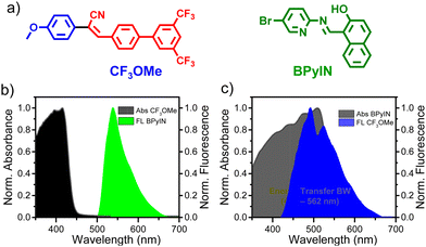 | ||
| Fig. 1 (a) Molecular structures of CF3OMe and BPyIN. (b and c) Solid-state absorption and emission spectra of CF3OMe and BPyIN. | ||
In this work, we report the design and synthesis of an efficient blue emissive CF3OMe flexible crystal. The molecular origin of the CF3OMe crystal's flexibility is established from a supramolecular perspective. The micromechanical and photonic properties are explored to utilize CF3OMe crystals for the construction of HDCs. CF3OMe and BPyIN were integrated on a single borosilicate chip (coverslip) by transferring a BPyIN crystal to the substrate containing CF3OMe crystal via a mechanophotonics approach. The constructed HDC implements multiple functions, acting as (i) an optical beam splitter (λ2; only green), and (ii) a direction- and (iii) signal-modulator (λ1 and λ2; blue and green) when BPyIN or CF3OMe crystals receive the same input light.
Results and discussion
The desired CF3OMe molecule was synthesized in 65% yield following the base condensation reaction (ESI;† Scheme S1 and Fig. S1). The optical absorption spectrum of CF3OMe consisted of a λmax at ≈ 425 nm with a tail extending up to ≈ 475 nm. The optical emission of BPyIN extended to ≈ 560 nm with λmax at ≈ 525 nm (Fig. 1b). The fluorescence (FL) spectrum of CF3OMe covered the 420–660 nm region with a maximum centered at ≈ 475 nm (Fig. 1c). The FL of CF3OMe has maximum overlap covering the ≈ 422–562 nm absorption region of BPyIN suggesting substantial radiative energy transfer (ET) from CF3OMe to BPyIN. However, there is no significant overlap between the absorption of CF3OMe and emission of BPyIN. The brilliant FL (τFL = 2.95 ns, Fig. S2, ESI†) of CF3OMe corroborated well with a solid-state photoluminescence quantum yield of 0.36, measured using an integrated sphere setup. The PLQY of the BPyIN crystal was recorded to be 16.7%.25The fiber-like crystals of CF3OMe were grown from dichloromethane![[thin space (1/6-em)]](https://www.rsc.org/images/entities/char_2009.gif) :
:![[thin space (1/6-em)]](https://www.rsc.org/images/entities/char_2009.gif) methanol (1
methanol (1![[thin space (1/6-em)]](https://www.rsc.org/images/entities/char_2009.gif) :
:![[thin space (1/6-em)]](https://www.rsc.org/images/entities/char_2009.gif) 1) solution at room temperature by slow evaporation method. The molecule crystalized in a triclinic system with the P
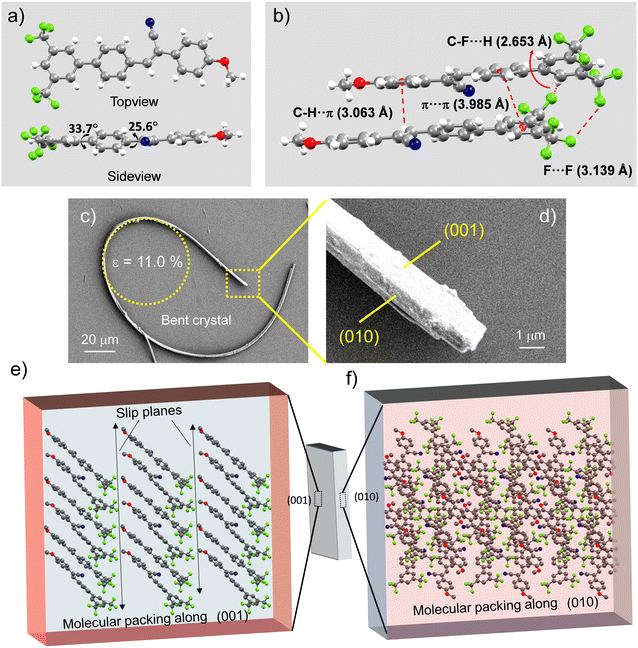
1) solution at room temperature by slow evaporation method. The molecule crystalized in a triclinic system with the P![[1 with combining macron]](https://www.rsc.org/images/entities/char_0031_0304.gif) space group (CCDC 2222211†). The torsional angle of the D and A moieties with respect to the π spacer is 33.7° and 25.6°, respectively (Fig. 2a). The rich non-covalent interactions like type-I halogen interactions40 between fluorine atoms, hydrogen bonding between the electronegative fluorine and hydrogen atoms (C–F⋯H: ≈ 2.653 Å), π⋯π (≈ 3.985 Å) interactions among stacked layers and C–H⋯π (≈ 3.063 Å) interactions enable anisotropic molecular packing in the CF3OMe crystals (Fig. 2b). These diverse weak and dispersive molecular interactions allow the crystal to possess strain withstanding capabilities without fatigue. The field emission scanning electron micrograph (FESEM) shows a naturally bent CF3OMe crystal accumulating a strain of 11% at the curved portion (Fig. 2c). This illustrates the strain holding capacity of the CF3OMe crystal supported by abundant non-covalent interactions. A closer view suggests rectangular features of the bent crystal (Fig. 2d). The face-indexing and growth morphology predictions confirmed the wider and thinner faces corresponding to the (001) and (010) planes, respectively (Fig. 2e and f).
space group (CCDC 2222211†). The torsional angle of the D and A moieties with respect to the π spacer is 33.7° and 25.6°, respectively (Fig. 2a). The rich non-covalent interactions like type-I halogen interactions40 between fluorine atoms, hydrogen bonding between the electronegative fluorine and hydrogen atoms (C–F⋯H: ≈ 2.653 Å), π⋯π (≈ 3.985 Å) interactions among stacked layers and C–H⋯π (≈ 3.063 Å) interactions enable anisotropic molecular packing in the CF3OMe crystals (Fig. 2b). These diverse weak and dispersive molecular interactions allow the crystal to possess strain withstanding capabilities without fatigue. The field emission scanning electron micrograph (FESEM) shows a naturally bent CF3OMe crystal accumulating a strain of 11% at the curved portion (Fig. 2c). This illustrates the strain holding capacity of the CF3OMe crystal supported by abundant non-covalent interactions. A closer view suggests rectangular features of the bent crystal (Fig. 2d). The face-indexing and growth morphology predictions confirmed the wider and thinner faces corresponding to the (001) and (010) planes, respectively (Fig. 2e and f).
To validate the mechanical flexibility of the CF3OMe crystals, a three-point bending test was performed with the help of a needle and forceps (Fig. S3a–e, ESI†). The long crystals of CF3OMe could be reversibly bent multiple times without any observable damage (Fig. S3f, ESI†). Interestingly, the crystals exhibited enhanced flexibility with water as a lubricant. The molecular origin of the mechanical flexibility can be understood from robust supramolecular interactions in the crystal packing. The molecular packing along the (001) plane shows a periodic layered arrangement of CF3OMe molecules giving rise to slip planes along the [010] direction (Fig. 2e). These slip planes possibly assist the gentle to-and-fro motion of atoms or minute reversible sliding to support stress disbursal. Therefore, when the crystal experiences mechanical force perpendicular to the (001) plane, it performs reversible elastic deformation. However, due to the absence of stress disbursal mechanisms along other thinner faces like (010) plane, the crystal breaks when stress is applied perpendicular to this plane, explaining the anisotropic nature of the crystal packing (Fig. 2f). Topical developments in the field of mechanophotonics unraveled the peculiar behavior of the crystals in the micro-regime.1,2 The demonstration of the pseudo-plasticity of the (elastic) microcrystals reiterates the influence of the crystal's aspect ratio and their adhesive interaction with the substrate (borosilicate). This pseudo-plasticity observed in CF3OMe and BPyIN was ingeniously utilized to fabricate crystal-based miniature optical components and devices.
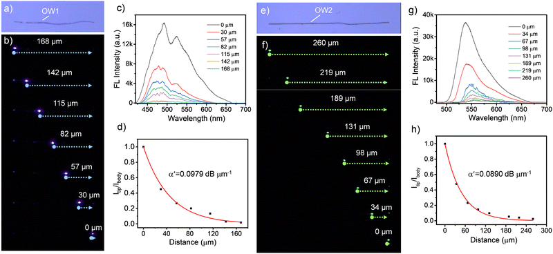
The microcrystals of CF3OMe and BPyIN were prepared by the self-assembly method (details are provided in ESI†). The crystallinity of the CF3OMe microstructures was confirmed from the selected area electron diffraction performed using transmission electron microscopy (Fig. S4, ESI†). The micromechanical manipulation and photonic studies were performed on a confocal optical microscope attached with an AFM cantilever tip. For optical excitation of the crystal terminal, a 60× objective was used, whereas a 20× objective was utilized for recording the spectra and images. The optical properties of the CF3OMe microcrystal (OW1) of length, L ≈ 168 μm was studied by illuminating the left terminal with a 405 nm continuous wave laser (Fig. 3a and b). At the point of excitation, blue FL of CF3OMe with a bandwidth λ1 ≈ 420–670 nm was produced. As the generated light propagates towards the crystal's opposite terminal, because of reabsorption, the resultant emission spectrum corresponds to a narrow band signal, −λ1 ≈ 440–670 nm (Fig. 3c). Importantly, the FL spectrum at the terminal of OW1 comprised of sharp peaks called optical modes. The optical modes in CF3OMe arise because of back-and-forth reflection of confined FL within the crystal cavity. The typical free spectral range (FSR), the spacing between two consecutive modes, was calculated to be ≈ 11 nm at λmax. The light guiding efficiency of the CF3OMe waveguide can be understood from its optical loss. The FL spectrum collected at a fixed end for varied excitation positions along the longitudinal axis of the microcrystal waveguide can be used to calculate the optical loss coefficient (α′). The α′ for the CF3OMe waveguide of L ≈ 168 μm was estimated to be 0.0979 dB μm−1 (Fig. 3d). Similar photonic investigations were carried out on a BPyIN crystal (L ≈ 260 μm, OW2, Fig. 3e). Laser light irradiation on OW2's left terminal produced a green FL with a bandwidth λ2 ≈ 482–700 nm (Fig. 3f). The reabsorption in the BPyIN microcrystal resulted in a narrow bandwidth spectrum (−λ2 ≈ 532–700 nm) at the right terminal (Fig. 3g). The α′ of OW2 was estimated to be 0.0890 dB μm−1 (Fig. 3g and h). The FL spectrum collected at the right terminal of OW2 also consisted of optical modes akin to the CF3OMe crystal due to its smooth light-reflecting crystal facets.
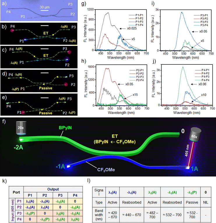
The previously reported organic directional couplers comprised uniformly strained structures.23,24 Here, we intended to construct a non-uniformly strained HDC, structurally close to the conventional silicon-type DC but with two chromatically different FL crystals. For that, a BPyIN microcrystal must be lifted from one substrate and released near the CF3OMe microcrystal in another substrate using an AFM cantilever tip close to the circuit construction site.1,2 The construction of a non-uniformly strained HDC was achieved by bending the BPyIN microcrystal at 135 and 186 μm from the left terminal of the microcrystal (Fig. 4a and Fig. S5a–h, ESI†). The strain created at these bent regions reached to 1.3% and 3.4%, respectively (Fig. S5i, ESI†). Apart from geometrical change, because of the change in molecular arrangement at the periphery of the strained microcrystal, slight variation in the refractive index (n) at the convex and concave parts of the crystal is possible. As a result, the light-confining nature of the cavity is perturbed and leads to changes in optical modes relative to the unstrained waveguide.26,31 The bent BPyIN microcrystal was slowly pushed in the forward direction with an AFM tip towards the CF3OMe microcrystal by moving the piezo stage (Fig. 4b–d). Later, the CF3OMe microcrystal was pushed in the x and y directions to bring them into evanescent contact with the BPyIN microcrystal (Fig. 4e and f). Then, the nearly straight CF3OMe crystal was slowly moved in the forward direction on the right side, followed by the same on the left side to bend it further away from the BPyIN microcrystal to achieve a non-uniformly strained HDC (Fig. 4g–m). The FL image (wide-field illumination) of the HDC shows four bright termini ascertaining the light guiding tendency of the microcrystals in contact (Fig. 4n). The color-coded FESEM image illustrates the bent geometries of both waveguides with a thickness of ≈ 0.92 and ≈ 1.87 μm for BPyIN and CF3OMe crystals, respectively (Fig. 4o). The zoomed-in view of the coupling region depicts close contact between the microcrystals. Hence, effective optical communication can be expected from one microcrystal to another. The optical signal processing and subsequent light routing capabilities of the constructed HDC were investigated by giving a 405 nm light input at any one of the microcrystal terminals or ports (abbreviated as P) and recording the FL signal response at the other three ports (Fig. 5a). For example, when the input was given at P1, it produced an active (A) blue FL signal (λ1(A); ≈420–670 nm) corresponding to CF3OMe (Fig. 5b and g). As the produced active signal propagates towards P2, due to the optical reabsorption, a narrow bandwidth signal (−λ1(A); ≈440–670 nm) outcoupled at P2 (Fig. 5g and l). Additionally, when the λ1(A) signal moves towards P2, its evanescent field excites the BPyIN microcrystal via ET in the coupling region. Thus, the active green FL signal (−λ2(A); ≈482–700 nm) generated in the BPyIN waveguide near the coupling region propagates to P3 (Fig. 5k and l). No light output signal (0) was recorded at P3 due to the circuit's directional coupling geometry (Fig. 5l). Similarly, for light input at P2, signals −λ1(A), −λ2(A) and 0 were spectroscopically recorded at P1, P4 and P3, respectively (Fig. 5c and h). The graphics presented in Fig. 5f clearly depict the light splitting and outcoupling of two chromatically different active signals (λ2 and λ1) in the forward direction by the HDC.
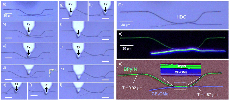 | ||
| Fig. 4 (a–l) Steps involved in the mechanical integration of bent BPyIN with the CF3OMe microcrystal to fabricate a hybrid directional coupler (HDC). (m) Confocal optical, (n) FL and (o) colour-coded FESEM images of the HDC. The inset in Fig. 4o shows a magnified view of the physical coupling between the two microcrystals. T stands for thickness. The scale bar corresponds to 30 μm. | ||
Furthermore, when light input is given to BPyIN (OW2) at P3, a bright green FL signal (λ2; ≈482–700 nm) is produced at the point of excitation (Fig. 5d and i). The FL signal is reabsorbed and a narrow band active signal (−λ2; ≈532–700 nm) was outcoupled at P4 (Fig. 5l). The same signal is split at the coupling region due to evanescent coupling with OW1 and passively (P) propagated as a −λ2(P) signal towards P1 as there is no ET possibility from BPyIN to CF3OMe. Meanwhile, no signal output is detected at P2 due to the circuit directionality. Similarly, for the input signal at P4, the −λ2(A), −λ2(P) and 0 signals were outcoupled at P3, P2 and P1, respectively (Fig. 5e and j).
Therefore, providing laser input to any one of the ports of the CF3OMe crystal waveguide in the HDC results in chromaticity modulation-and-splitting of the signal in the same circuit. While the same laser input given at any of the ports of the BPyIN waveguide results only in splitting the signal (λ2) without any chromaticity modulation. Hence, the fabricated HDC acts as an input-selective optical signal splitter/color modulator, demonstrating the multi-tasking capabilities within the same circuit. Furthermore, the optical modes observed in the individual waveguides were distinctly modified in the HDC at the respective ports relative to the uncoupled waveguides. This is due to the interference of the optical signals at the evanescent coupling region (Fig. S6, ESI†).
Conclusion
In summary, we designed and synthesized an efficient blue-emitting CF3OMe molecule. Crystallization of the CF3OMe molecules produced mechanically elastic crystals. The blue-emitting CF3OMe crystal in combination with a green-emitting elastic crystal was employed to construct a hybrid 2 × 2 directional coupler (HDC). For this, the microcrystals of CF3OMe and BPyIN were integrated into a single substrate by transferring the BPyIN crystals from one substrate to another close to the circuit fabrication site using the mechanophotonics approach. The photonic studies demonstrated the signal input-terminal dependent diverse optical functioning of the HDC. The HDC acted as a signal chromaticity modulator-and-splitter (λ1 and λ2; blue and green) in one case and as a simple beam splitter in another case (λ2; green). Therefore, the HDC exhibited multi-tasking capabilities with a single geometry because of the innovative inclusion of two different FL flexible crystals. Developing such pioneering optical components has broader implications for the advancement of flexible photonic device applications, in particular organic neural networks and neuromorphic photonic technologies.Conflicts of interest
The authors declare no conflict of interest.Acknowledgements
This work was financially supported UoH-IoE (UoH/RC1/RC1/20-003).References
- R. Chandrasekar, Chem. Commun., 2022, 58, 3415–3428 RSC.
- R. Chandrasekar, Small, 2021, 17, 2100277 CrossRef CAS PubMed.
- K. Takazawa, J. Inoue, K. Mitsuishi and T. Takamasu, Phys. Rev. Lett., 2010, 105, 067401 CrossRef PubMed.
- H. Dong, Y. Wei, W. Zhang, C. Wei, C. Zhang, J. Yao and Y. S. Zhao, J. Am. Chem. Soc., 2016, 138, 1118 CrossRef CAS PubMed.
- U. Venkataramudu, M. Annadhasan, H. Maddali and R. Chandrasekar, J. Mater. Chem. C, 2017, 5, 7262–7269 RSC.
- C. Zhang, C.-L. Zou, Y. Yan, R. Hao, F.-W. Sun, Z.-F. Han, Y. S. Zhao and J. Yao, J. Am. Chem. Soc., 2011, 133, 7276 CrossRef CAS PubMed.
- N. Mitetelo, D. Venkatakrishnarao, J. Ravi, M. Popov, E. Mamonov, T. V. Murzina and R. Chandrasekar, Adv. Opt. Mater., 2019, 7, 1801775 CrossRef.
- M. Annadhasan, D. P. Karothu, R. Chinnasamy, E. Ahmed, L. Catalano, S. Ghosh, P. Naumov and R. Chandrasekar, Angew. Chem., Int. Ed., 2020, 59, 13821 CrossRef CAS PubMed.
- H. Liu, Z. Bian, Q. Cheng, L. Lan, Y. Wang and H. Zhang, Chem. Sci., 2019, 10, 227 RSC.
- U. Venkataramudu, C. Sahoo, S. Leelashree, M. Venkatesh, D. Ganesh, S. R. G. Naraharisetty, A. K. Chaudhary, S. Srinath and R. Chandrasekar, J. Mater. Chem. C, 2018, 6, 9330 RSC.
- N. Mitetelo, J. Ravi, S. Mondal, U. Venkataramudu, E. Mamonov, M. Popov, A. Maydykovskiy, G. Vaitheeswaran, T. Murzina and R. Chandrasekar, Adv. Opt. Mater., 2022 DOI:10.1002/adom.202201635.
- K. Takazawa, Y. Kitahama, Y. Kimura and G. Kido, Nano Lett., 2005, 5, 1293 CrossRef CAS PubMed.
- M. Annadhasan, S. Basak, N. Chandrasekhar and R. Chandrasekar, Adv. Opt. Mater., 2020, 8, 2000959 CrossRef CAS.
- S. Ghosh and C. M. Reddy, Angew. Chem., Int. Ed., 2012, 51, 10319 CrossRef CAS PubMed.
- N. Chandrasekhar, M. A. Mohiddon and R. Chandrasekar, Adv. Opt. Mater., 2013, 1, 305 CrossRef.
- L. Catalano, D. P. Karothu, S. Schramm, E. Ahmed, R. Rezgui, T. J. Barber, A. Famulari and P. Naumov, Angew. Chem., Int. Ed., 2018, 57, 17254–17258 CrossRef CAS PubMed.
- P. Naumov, S. Chizhik, M. K. Panda, N. K. Nath and E. Boldyreva, Chem. Rev., 2015, 115, 12440 CrossRef CAS PubMed.
- A. Worthy, A. Grosjean, M. C. Pfrunder, Y. Xu, C. Yan, G. Edwards, J. K. Clegg and J. C. McMurtrie, Nat. Chem., 2018, 10, 65 CrossRef CAS PubMed.
- B. Liu, Z. Lu, B. Tang, H. Liu, H. Liu, Z. Zhang, K. Ye and H. Zhang, Angew. Chem., Int. Ed., 2020, 59, 23117 CrossRef CAS PubMed.
- A. V. Kumar, M. Rohullah, J. Ravi, M. Godumala, M. Annadhasan and R. Chandrasekar, CrystEngComm, 2021, 23, 5774–5779 RSC.
- D. P. Karothu, G. Dushaq, E. Ahmed, L. Catalano, S. Polavaram, R. Ferreira, L. Li, S. Mohamed, M. Rasras and P. Naumov, Nat. Commun., 2021, 12, 1326 CrossRef CAS PubMed.
- J. Ravi, M. Annadhasan, A. V. Kumar and R. Chandrasekar, Adv. Funct. Mater., 2021, 31, 2100642 CrossRef CAS.
- J. Ravi and R. Chandrasekar, Adv. Opt. Mater., 2021, 9, 2100550 CrossRef CAS.
- K. Takazawa, J. Inoue, K. Mitsuishi and Y. Kuroda, Adv. Funct. Mater., 2013, 23, 839–845 CrossRef CAS.
- A. V. Kumar and R. Chandrasekar, Adv. Opt. Mater., 2022, 202201009 Search PubMed.
- K. Takazawa, J.-I. Inoue, K. Mitsuishi and T. Takamasu, Adv. Mater., 2011, 23, 3659 CrossRef CAS PubMed.
- D. Venkatakrishnarao, M. A. Mohiddon, N. Chandrasekhar and R. Chandrasekar, Adv. Opt. Mater., 2015, 3, 1035–1040 CrossRef CAS.
- Y. S. Zhao, A. Peng, H. Fu, Y. Ma and J. Yao, Adv. Mater., 2008, 20, 1661–1665 CrossRef CAS.
- V. Zhang, J. Yao and Y. S. Zhao, Acc. Chem. Res., 2016, 49, 1691–1700 CrossRef PubMed.
- A. V. Kumar, E. Mamonov, T. Murzina and R. Chandrasekar, Adv. Opt. Mater., 2022 DOI:10.1002/adom.202201507.
- A. V. Kumar, M. Godumala, J. Ravi and R. Chnadrasekar, Angew. Chem., Int. Ed., 2022, 61, e202212382 CAS.
- J. Ravi, A. V. Kumar, D. P. Karothu, M. Annadhasan, P. Naumov and R. Chandrasekar, Adv. Funct. Mater., 2021, 31, 2105415 CrossRef CAS.
- M. Annadhasan, A. R. Agrawal, S. Bhunia, V. V. Pradeep, S. S. Zade, C. M. Reddy and R. Chandrasekar, Angew. Chem., Int. Ed., 2020, 59, 13852 CrossRef CAS PubMed.
- M. Annadhasan, V. V. Pradeep, A. V. Kumar, J. Ravi and R. Chandrasekar, Small Struct., 2022, 3, 2100163 CrossRef CAS.
- Q. Lv, X. D. Wang, Y. Yu, M. P. Zhuo, M. Zheng and L. S. Liao, Nat. Commun., 2022, 13, 3099 CrossRef CAS PubMed.
- S. Chen, X. D. Wang, M. P. Zhou, Q. Lv, J. F. Liu and L. S. Zhao, Sci. China: Chem., 2022, 65, 740–745 CAS.
- Q. Lv and X. D. Wang, Sci. Bull., 2022, 67, 991–994 CrossRef CAS PubMed.
- M. P. Zhuo, Y. Su, Y. K. Qu, S. Chen, G. P. He, Y. Yuan, H. Liu, Y. Tao, X. D. Wang and L. S. Liao, Adv. Mater., 2021, 33, 2102719 CrossRef CAS PubMed.
- J. Wu, M. P. Zhou, R. Lai, S. N. Zou, C. C. Yan, Y. Yuan, S. Y. Yang, G. Q. Wei, X. D. Wang and L. S. Liao, Angew. Chem., Int. Ed., 2021, 60, 9114 CrossRef CAS PubMed.
- G. R. Desiraju, P. S. Ho, L. Kloo, A. C. Legon, R. Marquardt, P. Metrangolo, P. Politzer, G. Resnati and K. Rissanen, Pure Appl. Chem., 2013, 85, 1711–1713 CrossRef CAS.
Footnote |
| † Electronic supplementary information (ESI) available. CCDC 2222211. For ESI and crystallographic data in CIF or other electronic format see DOI: https://doi.org/10.1039/d2tc05044g |
| This journal is © The Royal Society of Chemistry 2023 |

